CN100382261C - 电荷发生半导体基板用凸起形成装置、电荷发生半导体基板的除静电方法、电荷发生半导体基板用除静电装置、及电荷发生半导体基板 - Google Patents
电荷发生半导体基板用凸起形成装置、电荷发生半导体基板的除静电方法、电荷发生半导体基板用除静电装置、及电荷发生半导体基板 Download PDFInfo
- Publication number
- CN100382261C CN100382261C CNB008098964A CN00809896A CN100382261C CN 100382261 C CN100382261 C CN 100382261C CN B008098964 A CNB008098964 A CN B008098964A CN 00809896 A CN00809896 A CN 00809896A CN 100382261 C CN100382261 C CN 100382261C
- Authority
- CN
- China
- Prior art keywords
- semiconductor substrate
- charge
- generating semiconductor
- temperature
- wafer
- Prior art date
- Legal status (The legal status is an assumption and is not a legal conclusion. Google has not performed a legal analysis and makes no representation as to the accuracy of the status listed.)
- Expired - Fee Related
Links
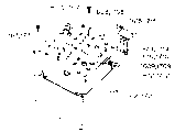
Images


Classifications
-
- H—ELECTRICITY
- H10—SEMICONDUCTOR DEVICES; ELECTRIC SOLID-STATE DEVICES NOT OTHERWISE PROVIDED FOR
- H10W—GENERIC PACKAGES, INTERCONNECTIONS, CONNECTORS OR OTHER CONSTRUCTIONAL DETAILS OF DEVICES COVERED BY CLASS H10
- H10W72/00—Interconnections or connectors in packages
- H10W72/071—Connecting or disconnecting
-
- H—ELECTRICITY
- H10—SEMICONDUCTOR DEVICES; ELECTRIC SOLID-STATE DEVICES NOT OTHERWISE PROVIDED FOR
- H10P—GENERIC PROCESSES OR APPARATUS FOR THE MANUFACTURE OR TREATMENT OF DEVICES COVERED BY CLASS H10
- H10P72/00—Handling or holding of wafers, substrates or devices during manufacture or treatment thereof
- H10P72/04—Apparatus for manufacture or treatment
- H10P72/0446—Apparatus for mounting on conductive members, e.g. leadframes or conductors on insulating substrates
-
- H—ELECTRICITY
- H10—SEMICONDUCTOR DEVICES; ELECTRIC SOLID-STATE DEVICES NOT OTHERWISE PROVIDED FOR
- H10P—GENERIC PROCESSES OR APPARATUS FOR THE MANUFACTURE OR TREATMENT OF DEVICES COVERED BY CLASS H10
- H10P72/00—Handling or holding of wafers, substrates or devices during manufacture or treatment thereof
- H10P72/04—Apparatus for manufacture or treatment
- H10P72/0444—Apparatus for wiring semiconductor or solid-state device
-
- Y—GENERAL TAGGING OF NEW TECHNOLOGICAL DEVELOPMENTS; GENERAL TAGGING OF CROSS-SECTIONAL TECHNOLOGIES SPANNING OVER SEVERAL SECTIONS OF THE IPC; TECHNICAL SUBJECTS COVERED BY FORMER USPC CROSS-REFERENCE ART COLLECTIONS [XRACs] AND DIGESTS
- Y10—TECHNICAL SUBJECTS COVERED BY FORMER USPC
- Y10S—TECHNICAL SUBJECTS COVERED BY FORMER USPC CROSS-REFERENCE ART COLLECTIONS [XRACs] AND DIGESTS
- Y10S438/00—Semiconductor device manufacturing: process
- Y10S438/974—Substrate surface preparation
Landscapes
- Wire Bonding (AREA)
- Container, Conveyance, Adherence, Positioning, Of Wafer (AREA)
- Micromachines (AREA)
- Light Receiving Elements (AREA)
- Solid State Image Pick-Up Elements (AREA)
- Exposure Of Semiconductors, Excluding Electron Or Ion Beam Exposure (AREA)
Applications Claiming Priority (11)
| Application Number | Priority Date | Filing Date | Title |
|---|---|---|---|
| JP1999/189053 | 1999-07-02 | ||
| JP18905399 | 1999-07-02 | ||
| JP29370299 | 1999-10-15 | ||
| JP1999/293702 | 1999-10-15 | ||
| JP1999/308855 | 1999-10-29 | ||
| JP30885599A JP3655787B2 (ja) | 1999-07-02 | 1999-10-29 | 電荷発生基板用バンプ形成装置及び電荷発生基板の除電方法 |
| JP32397999 | 1999-11-15 | ||
| JP1999/323979 | 1999-11-15 | ||
| JP2000184467A JP4570210B2 (ja) | 1999-07-02 | 2000-06-20 | 電荷発生基板用バンプ形成装置 |
| JP2000/184467 | 2000-06-20 | ||
| PCT/JP2000/004280 WO2001003176A1 (en) | 1999-07-02 | 2000-06-29 | Electric charge generating semiconductor substrate bump forming device, method of removing electric charge from electric charge generating semiconductor substrate, device for removing electric charge from electric charge generating semiconductor substrate, and electric charge generating semiconductor substrate |
Publications (2)
| Publication Number | Publication Date |
|---|---|
| CN1359534A CN1359534A (zh) | 2002-07-17 |
| CN100382261C true CN100382261C (zh) | 2008-04-16 |
Family
ID=27528983
Family Applications (1)
| Application Number | Title | Priority Date | Filing Date |
|---|---|---|---|
| CNB008098964A Expired - Fee Related CN100382261C (zh) | 1999-07-02 | 2000-06-29 | 电荷发生半导体基板用凸起形成装置、电荷发生半导体基板的除静电方法、电荷发生半导体基板用除静电装置、及电荷发生半导体基板 |
Country Status (7)
| Country | Link |
|---|---|
| US (3) | US6818975B1 (de) |
| EP (1) | EP1202336B1 (de) |
| KR (1) | KR100446262B1 (de) |
| CN (1) | CN100382261C (de) |
| AT (1) | ATE379847T1 (de) |
| DE (1) | DE60037251T2 (de) |
| WO (1) | WO2001003176A1 (de) |
Families Citing this family (15)
| Publication number | Priority date | Publication date | Assignee | Title |
|---|---|---|---|---|
| JP4456234B2 (ja) * | 2000-07-04 | 2010-04-28 | パナソニック株式会社 | バンプ形成方法 |
| US20030209310A1 (en) * | 2002-05-13 | 2003-11-13 | Fuentes Anastacio C. | Apparatus, system and method to reduce wafer warpage |
| JP4206320B2 (ja) | 2003-09-19 | 2009-01-07 | 株式会社ルネサステクノロジ | 半導体集積回路装置の製造方法 |
| US8296933B2 (en) * | 2008-08-19 | 2012-10-30 | Zamtec Limited | Fastening apparatus with authentication system |
| US8020281B2 (en) * | 2008-08-19 | 2011-09-20 | Silverbrook Research Pty Ltd | Printed circuit board bonding device |
| CN102426412A (zh) * | 2011-07-12 | 2012-04-25 | 上海华力微电子有限公司 | 一种掩模板表面微尘去除的方法 |
| US8324783B1 (en) | 2012-04-24 | 2012-12-04 | UltraSolar Technology, Inc. | Non-decaying electric power generation from pyroelectric materials |
| US10406580B2 (en) | 2013-11-15 | 2019-09-10 | Greenlee Tools, Inc. | Automated bender and systems and methods for providing data to operate an automated bender |
| JP6077023B2 (ja) * | 2015-01-09 | 2017-02-08 | 株式会社伸興 | 静電気除去装置及び静電気除去方法 |
| JP6456768B2 (ja) * | 2015-05-18 | 2019-01-23 | 株式会社ディスコ | 加工装置 |
| WO2018013271A1 (en) * | 2016-07-13 | 2018-01-18 | Applied Materials, Inc. | An improved substrate support |
| EP3506340B1 (de) * | 2017-12-28 | 2020-10-21 | Nexperia B.V. | Verbindungs- und indexierungsvorrichtung |
| US11735438B2 (en) * | 2018-12-03 | 2023-08-22 | Applied Materials, Inc. | Methods and apparatus for Marangoni drying |
| JP7489865B2 (ja) * | 2020-08-24 | 2024-05-24 | 東京エレクトロン株式会社 | 基板処理方法及び基板処理装置 |
| CN120316993B (zh) * | 2025-04-03 | 2026-03-03 | 惠州中科智能科技有限公司 | 大数据驱动的无尘拖链抗静电优化设计方法 |
Citations (1)
| Publication number | Priority date | Publication date | Assignee | Title |
|---|---|---|---|---|
| US5341979A (en) * | 1993-09-03 | 1994-08-30 | Motorola, Inc. | Method of bonding a semiconductor substrate to a support substrate and structure therefore |
Family Cites Families (23)
| Publication number | Priority date | Publication date | Assignee | Title |
|---|---|---|---|---|
| JPS5925370B2 (ja) | 1978-12-26 | 1984-06-16 | 富士通株式会社 | 半導体装置の製造方法 |
| JPS62173428A (ja) | 1986-01-28 | 1987-07-30 | Fujitsu Ltd | 導波路光デバイス |
| JPS6477111A (en) * | 1987-09-18 | 1989-03-23 | Fujikura Ltd | Removal of static electricity of wafer |
| JPH02203180A (ja) * | 1989-02-02 | 1990-08-13 | Sawafuji Electric Co Ltd | 冷却装置 |
| JPH03293808A (ja) * | 1990-04-11 | 1991-12-25 | Fujitsu Ltd | 弾性表面波素子の製造方法 |
| JPH0491422A (ja) * | 1990-08-01 | 1992-03-24 | Mitsubishi Electric Corp | 半導体装置の製造方法 |
| JPH06232132A (ja) | 1993-02-02 | 1994-08-19 | Toshiba Corp | バンプ形成装置 |
| US5665167A (en) | 1993-02-16 | 1997-09-09 | Tokyo Electron Kabushiki Kaisha | Plasma treatment apparatus having a workpiece-side electrode grounding circuit |
| US5719739A (en) * | 1994-01-13 | 1998-02-17 | Horiguchi; Noboru | Static eliminator |
| JP3339164B2 (ja) | 1994-02-16 | 2002-10-28 | 東レ株式会社 | 樹脂硬化tabテープの製造装置および製造方法 |
| JP3415283B2 (ja) * | 1994-08-31 | 2003-06-09 | 株式会社東芝 | バンプ形成装置、バンプ形成方法および半導体素子の製造方法 |
| JP3079921B2 (ja) * | 1994-11-28 | 2000-08-21 | 松下電器産業株式会社 | 半田ボールの搭載装置および搭載方法 |
| JPH1116874A (ja) | 1997-06-26 | 1999-01-22 | Nec Kansai Ltd | 遠心乾燥装置 |
| JPH1187392A (ja) * | 1997-09-09 | 1999-03-30 | Oki Electric Ind Co Ltd | バンプ形成方法 |
| JPH11168074A (ja) * | 1997-12-03 | 1999-06-22 | Hitachi Denshi Ltd | 圧電体基板のダイシング方法 |
| US6198616B1 (en) | 1998-04-03 | 2001-03-06 | Applied Materials, Inc. | Method and apparatus for supplying a chucking voltage to an electrostatic chuck within a semiconductor wafer processing system |
| US6056191A (en) * | 1998-04-30 | 2000-05-02 | International Business Machines Corporation | Method and apparatus for forming solder bumps |
| JPH11330573A (ja) * | 1998-05-11 | 1999-11-30 | Toyo Commun Equip Co Ltd | バンプ形成方法及びバンプ形成装置 |
| JP2000059165A (ja) * | 1998-08-06 | 2000-02-25 | Toshiba Corp | 弾性表面波装置およびその製造方法 |
| JP4203152B2 (ja) * | 1998-09-11 | 2008-12-24 | 株式会社日立メディアエレクトロニクス | 弾性表面波装置 |
| EP1133219A4 (de) * | 1998-10-13 | 2004-10-27 | Matsushita Electric Industrial Co Ltd | Heizvorrichtung und heizverfahren |
| JP2002009569A (ja) * | 2000-06-26 | 2002-01-11 | Toshiba Corp | 弾性表面波装置の製造方法 |
| JP2002203995A (ja) * | 2000-12-27 | 2002-07-19 | Toshiba Corp | 基板加熱方法、基板冷却方法、及びそれらの装置 |
-
2000
- 2000-06-29 US US10/019,700 patent/US6818975B1/en not_active Expired - Fee Related
- 2000-06-29 CN CNB008098964A patent/CN100382261C/zh not_active Expired - Fee Related
- 2000-06-29 KR KR10-2001-7016543A patent/KR100446262B1/ko not_active Expired - Fee Related
- 2000-06-29 DE DE60037251T patent/DE60037251T2/de not_active Expired - Fee Related
- 2000-06-29 EP EP00942389A patent/EP1202336B1/de not_active Expired - Lifetime
- 2000-06-29 AT AT00942389T patent/ATE379847T1/de not_active IP Right Cessation
- 2000-06-29 WO PCT/JP2000/004280 patent/WO2001003176A1/ja not_active Ceased
-
2003
- 2003-08-29 US US10/651,103 patent/US7014092B2/en not_active Expired - Fee Related
- 2003-08-29 US US10/651,199 patent/US7005368B1/en not_active Expired - Fee Related
Patent Citations (1)
| Publication number | Priority date | Publication date | Assignee | Title |
|---|---|---|---|---|
| US5341979A (en) * | 1993-09-03 | 1994-08-30 | Motorola, Inc. | Method of bonding a semiconductor substrate to a support substrate and structure therefore |
Also Published As
| Publication number | Publication date |
|---|---|
| US20040035849A1 (en) | 2004-02-26 |
| EP1202336A4 (de) | 2004-06-23 |
| EP1202336A1 (de) | 2002-05-02 |
| DE60037251T2 (de) | 2008-10-09 |
| US7014092B2 (en) | 2006-03-21 |
| DE60037251D1 (de) | 2008-01-10 |
| WO2001003176A1 (en) | 2001-01-11 |
| US6818975B1 (en) | 2004-11-16 |
| KR100446262B1 (ko) | 2004-09-01 |
| EP1202336B1 (de) | 2007-11-28 |
| ATE379847T1 (de) | 2007-12-15 |
| CN1359534A (zh) | 2002-07-17 |
| KR20020022076A (ko) | 2002-03-23 |
| US7005368B1 (en) | 2006-02-28 |
Similar Documents
| Publication | Publication Date | Title |
|---|---|---|
| CN100382261C (zh) | 电荷发生半导体基板用凸起形成装置、电荷发生半导体基板的除静电方法、电荷发生半导体基板用除静电装置、及电荷发生半导体基板 | |
| US5447886A (en) | Method for mounting semiconductor chip on circuit board | |
| CN1578600B (zh) | 部件接合装置及方法与部件安装装置 | |
| JP5572353B2 (ja) | 保護テープ剥離方法およびその装置 | |
| JP4456234B2 (ja) | バンプ形成方法 | |
| WO2005122237A1 (ja) | 部品実装方法及び部品実装装置 | |
| US20080179378A1 (en) | Method of forming bumps on a wafer utilizing a post-heating operation, and an apparatus therefore | |
| JP4570210B2 (ja) | 電荷発生基板用バンプ形成装置 | |
| JP3655787B2 (ja) | 電荷発生基板用バンプ形成装置及び電荷発生基板の除電方法 | |
| CN120854321A (zh) | 封装装置 | |
| JP4088628B2 (ja) | バンプ形成装置 | |
| US7508495B2 (en) | Positioning stage, bump forming apparatus equipped with the positioning stage, and bump forming method performed using the positioning stage | |
| US20050127141A1 (en) | Mounting method of bump-equipped electronic component and mounting structure of the same | |
| US11541472B2 (en) | Ultrasonic-assisted solder transfer | |
| JP4962445B2 (ja) | 基板搬出装置 | |
| TW202410211A (zh) | 安裝裝置及安裝方法 | |
| CN120730638A (zh) | 压接装置 | |
| JP2007012742A (ja) | 樹脂硬化装置および樹脂封止された半導体素子実装部品 |
Legal Events
| Date | Code | Title | Description |
|---|---|---|---|
| C10 | Entry into substantive examination | ||
| SE01 | Entry into force of request for substantive examination | ||
| C06 | Publication | ||
| PB01 | Publication | ||
| C14 | Grant of patent or utility model | ||
| GR01 | Patent grant | ||
| C17 | Cessation of patent right | ||
| CF01 | Termination of patent right due to non-payment of annual fee |
Granted publication date: 20080416 Termination date: 20100629 |