CN102738136A - Distributed high-voltage light emitting diode (LED) module - Google Patents
Distributed high-voltage light emitting diode (LED) module Download PDFInfo
- Publication number
- CN102738136A CN102738136A CN2012102045629A CN201210204562A CN102738136A CN 102738136 A CN102738136 A CN 102738136A CN 2012102045629 A CN2012102045629 A CN 2012102045629A CN 201210204562 A CN201210204562 A CN 201210204562A CN 102738136 A CN102738136 A CN 102738136A
- Authority
- CN
- China
- Prior art keywords
- led
- substrate
- module
- distributed high
- voltage
- Prior art date
- Legal status (The legal status is an assumption and is not a legal conclusion. Google has not performed a legal analysis and makes no representation as to the accuracy of the status listed.)
- Pending
Links
Images


Classifications
-
- H—ELECTRICITY
- H10—SEMICONDUCTOR DEVICES; ELECTRIC SOLID-STATE DEVICES NOT OTHERWISE PROVIDED FOR
- H10W—GENERIC PACKAGES, INTERCONNECTIONS, CONNECTORS OR OTHER CONSTRUCTIONAL DETAILS OF DEVICES COVERED BY CLASS H10
- H10W90/00—Package configurations
- H10W90/701—Package configurations characterised by the relative positions of pads or connectors relative to package parts
- H10W90/751—Package configurations characterised by the relative positions of pads or connectors relative to package parts of bond wires
- H10W90/753—Package configurations characterised by the relative positions of pads or connectors relative to package parts of bond wires between laterally-adjacent chips
Landscapes
- Led Device Packages (AREA)
Abstract
本发明公开了一种分布式高压LED模组,其包括基板、线路层及多个LED小模组,所述线路层固定在所述基板上,所述多个LED小模组间隔地排布在所述基板或所述线路层上,每个所述LED小模组包括多个LED芯片,该多个LED芯片之间进行串联和/或并联连接后与所述线路层进行电性连接,所述多个LED小模组之间进行串联和/或并联连接。本发明分布式高压LED模组将LED芯片封装成多个LED小模组,而后排布在基板或线路层上并进行串并联连接,基于该设计,本发明具有以下优点:热量分散,提高LED使用寿命;发光面分散,方便灯具配光;可达到110V以上高压,方便驱动设计;减小芯片与芯片之间的影响,光效高。
The invention discloses a distributed high-voltage LED module, which includes a substrate, a circuit layer and a plurality of small LED modules, the circuit layer is fixed on the substrate, and the plurality of small LED modules are arranged at intervals On the substrate or the circuit layer, each of the small LED modules includes a plurality of LED chips, and the plurality of LED chips are connected in series and/or in parallel and then electrically connected to the circuit layer, The plurality of small LED modules are connected in series and/or in parallel. The distributed high-voltage LED module of the present invention packages LED chips into a plurality of small LED modules, and then arranges them on the substrate or circuit layer and connects them in series and parallel. Based on this design, the present invention has the following advantages: heat dispersion, improved LED Long service life; the light-emitting surface is scattered, which is convenient for light distribution of lamps; it can reach high voltage above 110V, which is convenient for driving design; the influence between chips is reduced, and the light efficiency is high.
Description
技术领域 technical field
本发明涉及LED技术领域,更具体地涉及一种分布式高压LED模组。The invention relates to the technical field of LEDs, and in particular to a distributed high-voltage LED module.
背景技术 Background technique
目前,LED发光二极管由于具有耗电量低、环保节能等优点而得到社会各界的广泛关注和认可,众多相关的生产厂商积极响应国家提出的节能减排政策,在LED的研发和推广上做出了极大投入。At present, LED light-emitting diodes have been widely concerned and recognized by all walks of life due to their advantages of low power consumption, environmental protection and energy saving. great investment.
单个LED发光二极管功率小、发光量少,为了解决这个问题,市面上出现了由多个LED芯片组成的LED模组以获得照明所需功率和光通量。然而,现有的LED模组均为集成式,其出光面通常只有一个,不仅具有热量集中、光效低等缺陷,而且在利用其制作灯具或者光源的时候不好配光,不能很好满足市场需求。A single LED light-emitting diode has low power and low light output. In order to solve this problem, LED modules composed of multiple LED chips have appeared on the market to obtain the required power and luminous flux for lighting. However, the existing LED modules are all integrated, and there is usually only one light-emitting surface, which not only has defects such as heat concentration and low light efficiency, but also has poor light distribution when using them to make lamps or light sources, and cannot satisfy Market demand.
因此,有必要提供一种分布式高压LED模组以解决上述缺陷。Therefore, it is necessary to provide a distributed high-voltage LED module to solve the above defects.
发明内容 Contents of the invention
本发明的目的是提供一种分布式高压LED模组以满足市场需求。The purpose of the present invention is to provide a distributed high-voltage LED module to meet market demand.
为了实现上述目的,本发明采用的技术方案为:提供一种分布式高压LED模组,其包括基板、线路层及多个LED小模组,所述线路层固定在所述基板上,所述多个LED小模组间隔地排布在所述基板或所述线路层上,每个所述LED小模组包括多个LED芯片,该多个LED芯片之间进行串联和/或并联连接后与所述线路层进行电性连接,所述多个LED小模组之间进行串联和/或并联连接。In order to achieve the above purpose, the technical solution adopted by the present invention is to provide a distributed high-voltage LED module, which includes a substrate, a circuit layer and a plurality of small LED modules, the circuit layer is fixed on the substrate, and the A plurality of small LED modules are arranged at intervals on the substrate or the circuit layer, each of the small LED modules includes a plurality of LED chips, and the plurality of LED chips are connected in series and/or in parallel It is electrically connected with the circuit layer, and the plurality of small LED modules are connected in series and/or in parallel.
其进一步技术方案为:所述基板为金属基板,所述线路层上形成有多个用于排布所述LED小模组的镂空区,所述LED芯片固定在所述镂空区内的基板表面上。Its further technical solution is: the substrate is a metal substrate, a plurality of hollow areas for arranging the small LED modules are formed on the circuit layer, and the LED chips are fixed on the surface of the substrate in the hollow areas superior.
其进一步技术方案为:所述镂空区内的基板表面覆盖有一反射层。Its further technical solution is: the surface of the substrate in the hollow area is covered with a reflective layer.
其进一步技术方案为:所述反射层为银层。Its further technical solution is: the reflective layer is a silver layer.
其进一步技术方案为:所述LED小模组还包括一围坝装置,所述围坝装置设置在所述线路层上且位于所述镂空区的边缘,所述围坝装置内填充有封装胶。Its further technical solution is: the small LED module also includes a dam device, the dam device is arranged on the circuit layer and is located at the edge of the hollow area, and the dam device is filled with encapsulating glue .
在本发明的另一实施例中,所述基板为金属基板,所述线路层完全覆盖所述基板的上表面,所述LED芯片固定在所述线路层上。In another embodiment of the present invention, the substrate is a metal substrate, the circuit layer completely covers the upper surface of the substrate, and the LED chip is fixed on the circuit layer.
其进一步技术方案为:所述LED小模组还包括一围坝装置,所述围坝装置设置在所述线路层上,其内填充有封装胶。Its further technical solution is: the small LED module further includes a dam device, the dam device is arranged on the circuit layer, and is filled with encapsulation glue.
在本发明的再一实施例中,所述基板为陶瓷基板,所述LED芯片固定在所述陶瓷基板上,所述线路层为制作于所述陶瓷基板上的导电线路。In yet another embodiment of the present invention, the substrate is a ceramic substrate, the LED chip is fixed on the ceramic substrate, and the circuit layer is a conductive circuit fabricated on the ceramic substrate.
其进一步技术方案为:每个所述LED小模组还包括一围坝装置,所述围坝装置设置在所述陶瓷基板上,其内填充有封装胶。Its further technical solution is: each of the small LED modules further includes a dam device, the dam device is arranged on the ceramic substrate, and is filled with encapsulation glue.
其进一步技术方案为:所述封装胶为由硅胶和荧光粉混合而成的雾状胶体。Its further technical solution is: the encapsulating glue is a mist-like colloid formed by mixing silica gel and fluorescent powder.
与现有技术相比,本发明提供的分布式高压LED模组将LED芯片封装成多个LED小模组,而后间隔地排布在基板或线路层上并进行串并联连接,基于该设计,本发明具有以下优点:热量分散,提高LED使用寿命;发光面分散,方便灯具配光;减小芯片与芯片之间的影响,光效高。Compared with the prior art, the distributed high-voltage LED module provided by the present invention packages LED chips into multiple small LED modules, and then arranges them at intervals on the substrate or circuit layer and connects them in series and parallel. Based on this design, The invention has the following advantages: the heat is dispersed to improve the service life of the LED; the light-emitting surface is dispersed to facilitate the light distribution of the lamp; the influence between chips is reduced and the light efficiency is high.
通过以下的描述并结合附图,本发明将变得更加清晰,这些附图用于解释本发明的实施例。The present invention will become clearer through the following description in conjunction with the accompanying drawings, which are used to explain the embodiments of the present invention.
附图说明 Description of drawings
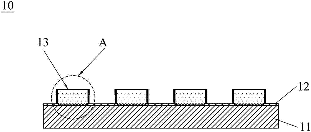
图1为本发明分布式高压LED模组第一实施例的剖面示意图。Fig. 1 is a schematic cross-sectional view of the first embodiment of the distributed high-voltage LED module of the present invention.
图2为图1所示分布式高压LED模组中A部分的放大图。Fig. 2 is an enlarged view of part A of the distributed high-voltage LED module shown in Fig. 1 .
图3为图1所示分布式高压LED模组的俯视图。Fig. 3 is a top view of the distributed high voltage LED module shown in Fig. 1 .
图4为本发明分布式高压LED模组第二实施例的剖面示意图。Fig. 4 is a schematic cross-sectional view of the second embodiment of the distributed high-voltage LED module of the present invention.
图5至图7展示了为本发明分布式高压LED模组的多种电路连接方式。5 to 7 show various circuit connection modes for the distributed high-voltage LED module of the present invention.
图8本发明分布式高压LED模组第三实施例的部分放大图。Fig. 8 is a partially enlarged view of the third embodiment of the distributed high-voltage LED module of the present invention.
图中各附图标记说明如下:The reference signs in the figure are explained as follows:
第一实施例:First embodiment:
分布式高压LED模组 10 基板 11Distributed high
线路层 12 LED小模组 13
围坝装置 131 封装胶 132
金属导线 133 LED芯片 134
第二实施例:Second embodiment:
分布式高压LED模组 20 基板 21Distributed high voltage LED module 20
线路层 22 LED小模组 23
第三实施例:Third embodiment:
分布式高压LED模组 30 基板 31Distributed high
导电线路 32 LED小模组 33
具体实施方式 Detailed ways
下面将结合本发明实施例中的附图,对实施例中的技术方案进行清楚、完整地描述,附图中类似的组件标号代表类似的组件。显然,以下将描述的实施例仅仅是本发明一部分实施例,而不是全部的实施例。基于本发明中的实施例,本领域普通技术人员在没有作出创造性劳动前提下所获得的所有其他实施例,都属于本发明保护的范围。The technical solutions in the embodiments of the present invention will be clearly and completely described below in conjunction with the drawings in the embodiments of the present invention, and similar component numbers in the drawings represent similar components. Apparently, the embodiments described below are only a part of the embodiments of the present invention, rather than all the embodiments. Based on the embodiments of the present invention, all other embodiments obtained by persons of ordinary skill in the art without creative efforts fall within the protection scope of the present invention.
首先请参照图1至图3,其展示了本发明分布式高压LED模组的第一实施例。本较佳实施例中,所述分布式高压LED模组10包括基板11、线路层12及多个LED小模组13,其中,所述基板11为金属基板,所述线路层12通过贴合的方式固定在基板11上,所述线路层12上形成有多个圆柱状的镂空区。First, please refer to FIG. 1 to FIG. 3 , which show the first embodiment of the distributed high voltage LED module of the present invention. In this preferred embodiment, the distributed high-
本实施例中,每个LED小模组13包括围坝装置131、封装胶132、金属导线133及多个LED芯片134,本实施例中,每个LED小模组13包括多于18颗的蓝光芯片。所述LED芯片134通过固晶胶固定在镂空区内的基板11上,LED芯片134固定在金属基板的设计可为LED芯片134带来更好的散热效果,优选地,位于镂空区内的基板11表面还镀有一反射层(未标示)以增强反射效果,本实施例选用具有高反射率的银层来作为反射层。In this embodiment, each
参照图2,本实施例的多个LED芯片134之间以及末端LED芯片134与线路层12之间均用金属导线133进行连接,线路层12上设置有中空圆柱状的围坝装置131,该围坝装置131固定在所述线路层12上且位于所述镂空区的边缘,其内填充有封装胶132,本实施例的封装胶132选用由硅胶和荧光粉混合而成的雾状胶体,从而可大大增加LED器件的可视角度。Referring to FIG. 2 ,
参照图3,本实施例的多个LED小模组13以一定的排列方式排布在基板11上,例如可设计为图3所示的矩阵式,也可根据具体实际需要设计为放射式等其它排布方式),相应地,线路层12上的镂空区是根据LED小模组13所需排布方式而进行相应的设计。Referring to FIG. 3 , a plurality of
参照图5至图7,对于LED小模组13内LED芯片134之间及LED小模组13之间的电路连接可通过以下方式来实现,但并不限于以下方式(每个虚线框内的所有器件组成一个LED小模组13):Referring to Fig. 5 to Fig. 7, the circuit connection between the
方式一:如图5所示,每个LED小模组13里面的LED芯片134全部进行串联,每两个LED小模组13再串联在一起,多组串联而成的模组再相互并联,采用此连接方式时,整个模组的电压可以达到110V以上。Method 1: As shown in Figure 5, all the
方式二:如图6所示,每个LED小模组13里面的LED芯片134先串联成三串再将其并联在一起,每两个LED小模组13相互串联在一起,多组串联而成的模组再相互并联,采用此连接方式时,整个模组的电压可以达到110V以上。Method 2: As shown in Figure 6, the
方式三:如图7所示,每个LED小模组13里面的LED芯片134全部进行串联,每四个LED小模组13再串联在一起,多组串联而成的模组再相互并联,采用此连接方式时,整个模组的电压可以达到220V以上。Method 3: As shown in FIG. 7 , all the
以此类推,本发明的分布式高压LED模组可采用多种不同的连接方式来实现不同的高压以满足用户或客户的不同需求。By analogy, the distributed high-voltage LED module of the present invention can adopt a variety of different connection methods to achieve different high voltages to meet the different needs of users or customers.
图4展示了本发明分布式高压LED模组的第二实施例。参照图4,本实施例分布式高压LED模组20与第一实施例的区别点在于:所述线路层22完全覆盖在所述金属基板21的上表面,每个LED小模组23是设置在线路层22上,即每个LED小模组23内的LED芯片是固定在线路层22上的,采用该结构设计相比第一实施例可方便电路连接,但散热效果不如第一实施例。Fig. 4 shows the second embodiment of the distributed high voltage LED module of the present invention. Referring to Fig. 4, the difference between the distributed high-voltage LED module 20 of this embodiment and the first embodiment is that: the
图8展示了本发明分布式高压LED模组的第三实施例。参照图8,本实施例分布式高压LED模组30与第一和第二实施例的区别点在于:所述基板31为陶瓷基板,陶瓷基板31的上表面通过蒸镀、印刷或者溅射等方式制作有导电线路32。在本实施例中,LED小模组33内的LED芯片是固定在陶瓷基板上31,每个小模组内上下均设置有导电线路,由多个LED芯片连接而成的LED串的两端用金属导线与导电线路连接。Fig. 8 shows the third embodiment of the distributed high voltage LED module of the present invention. Referring to FIG. 8 , the difference between the distributed high-
如上所述,本发明提供的分布式高压LED模组将LED芯片封装成多个LED小模组,而后排布在基板或线路层上并进行串并联连接,基于该设计,本发明具有以下优点:热量分散,提高LED使用寿命;发光面分散,方便灯具配光;可达到110V以上高压,方便驱动设计;减小芯片与芯片之间的影响,光效高;减少硅胶和荧光粉的使用量,降低成本。As mentioned above, in the distributed high-voltage LED module provided by the present invention, LED chips are packaged into multiple small LED modules, and then arranged on the substrate or circuit layer and connected in series and parallel. Based on this design, the present invention has the following advantages : Disperse the heat to improve the service life of LED; disperse the light-emitting surface to facilitate light distribution of lamps; can reach high voltage above 110V, which is convenient for driving design; reduce the influence between chips and increase luminous efficiency; reduce the use of silica gel and phosphor ,cut costs.
需要说明的是,在本发明分布式高压LED模组中,金属基板可选用铜基板、铝基板等金属基板;线路层除了贴合方式外,还可通过印刷、蒸镀或溅射等方式来制作在基板上;对于封装胶,也可单独选用透明的环氧树脂胶或硅胶来实现。It should be noted that in the distributed high-voltage LED module of the present invention, metal substrates such as copper substrates and aluminum substrates can be used as metal substrates; in addition to bonding methods, the circuit layer can also be printed, evaporated, or sputtered. It is made on the substrate; as for the encapsulation glue, it can also be realized by using transparent epoxy resin glue or silica gel alone.
以上结合最佳实施例对本发明进行了描述,但本发明并不局限于以上揭示的实施例,而应当涵盖各种根据本发明的本质进行的修改、等效组合。The present invention has been described above in conjunction with the best embodiments, but the present invention is not limited to the above-disclosed embodiments, but should cover various modifications and equivalent combinations made according to the essence of the present invention.
Claims (10)
Priority Applications (1)
| Application Number | Priority Date | Filing Date | Title |
|---|---|---|---|
| CN2012102045629A CN102738136A (en) | 2012-06-20 | 2012-06-20 | Distributed high-voltage light emitting diode (LED) module |
Applications Claiming Priority (1)
| Application Number | Priority Date | Filing Date | Title |
|---|---|---|---|
| CN2012102045629A CN102738136A (en) | 2012-06-20 | 2012-06-20 | Distributed high-voltage light emitting diode (LED) module |
Publications (1)
| Publication Number | Publication Date |
|---|---|
| CN102738136A true CN102738136A (en) | 2012-10-17 |
Family
ID=46993340
Family Applications (1)
| Application Number | Title | Priority Date | Filing Date |
|---|---|---|---|
| CN2012102045629A Pending CN102738136A (en) | 2012-06-20 | 2012-06-20 | Distributed high-voltage light emitting diode (LED) module |
Country Status (1)
| Country | Link |
|---|---|
| CN (1) | CN102738136A (en) |
Cited By (4)
| Publication number | Priority date | Publication date | Assignee | Title |
|---|---|---|---|---|
| CN103363357A (en) * | 2013-07-17 | 2013-10-23 | 晶科电子(广州)有限公司 | LED light source with well heat dissipation effect |
| CN104411111A (en) * | 2014-12-17 | 2015-03-11 | 江苏稳润光电有限公司 | Packaging process for LED nixie tubes |
| CN109802027A (en) * | 2019-02-22 | 2019-05-24 | 佛山市国星光电股份有限公司 | A kind of light source module group and its manufacturing method and its die cutting die |
| CN113628557A (en) * | 2021-06-29 | 2021-11-09 | 盐城市博时电子有限公司 | Distributed connection type LED crystal artistic photo frame |
Citations (4)
| Publication number | Priority date | Publication date | Assignee | Title |
|---|---|---|---|---|
| CN101416323A (en) * | 2006-04-10 | 2009-04-22 | 夏普株式会社 | LED assembly and lighting device and liquid crystal display device including the LED assembly |
| US20110062482A1 (en) * | 2010-01-20 | 2011-03-17 | Bridgelux, Inc. | Apparatus And Method For Enhancing Connectability In LED Array Using Metal Traces |
| WO2011122846A2 (en) * | 2010-03-31 | 2011-10-06 | 주식회사 포인트 엔지니어링 | Optical device and method for manufacturing same |
| WO2012002710A2 (en) * | 2010-06-30 | 2012-01-05 | 주식회사 포인트엔지니어링 | Optical element device |
-
2012
- 2012-06-20 CN CN2012102045629A patent/CN102738136A/en active Pending
Patent Citations (4)
| Publication number | Priority date | Publication date | Assignee | Title |
|---|---|---|---|---|
| CN101416323A (en) * | 2006-04-10 | 2009-04-22 | 夏普株式会社 | LED assembly and lighting device and liquid crystal display device including the LED assembly |
| US20110062482A1 (en) * | 2010-01-20 | 2011-03-17 | Bridgelux, Inc. | Apparatus And Method For Enhancing Connectability In LED Array Using Metal Traces |
| WO2011122846A2 (en) * | 2010-03-31 | 2011-10-06 | 주식회사 포인트 엔지니어링 | Optical device and method for manufacturing same |
| WO2012002710A2 (en) * | 2010-06-30 | 2012-01-05 | 주식회사 포인트엔지니어링 | Optical element device |
Cited By (5)
| Publication number | Priority date | Publication date | Assignee | Title |
|---|---|---|---|---|
| CN103363357A (en) * | 2013-07-17 | 2013-10-23 | 晶科电子(广州)有限公司 | LED light source with well heat dissipation effect |
| CN104411111A (en) * | 2014-12-17 | 2015-03-11 | 江苏稳润光电有限公司 | Packaging process for LED nixie tubes |
| CN109802027A (en) * | 2019-02-22 | 2019-05-24 | 佛山市国星光电股份有限公司 | A kind of light source module group and its manufacturing method and its die cutting die |
| CN109802027B (en) * | 2019-02-22 | 2024-04-09 | 佛山市国星光电股份有限公司 | Light source module, manufacturing method thereof and punching die thereof |
| CN113628557A (en) * | 2021-06-29 | 2021-11-09 | 盐城市博时电子有限公司 | Distributed connection type LED crystal artistic photo frame |
Similar Documents
| Publication | Publication Date | Title |
|---|---|---|
| JP2022002328A (en) | Light emitting module and manufacturing method thereof | |
| CN104253200A (en) | Light-emitting component and manufacturing method | |
| AU2012200375A1 (en) | Method for Packaging an LED Emitting Light Omnidirectionally and an LED Package | |
| CN104517947A (en) | Light emitting diode assembly and manufacturing method | |
| CN101696790A (en) | High-power LED heat-dissipation packaging structure | |
| CN102709281A (en) | Double fluorescent thin film two-sided light-emitting planar wafer LED (Light-Emitting Diode) array light source | |
| CN102709278A (en) | Plane thin sheet type LED (Light-Emitting Diode) array light source of fluorescent thin film | |
| CN203288644U (en) | Distributed high-voltage LED (Light-Emitting Diode) module group | |
| CN101859759A (en) | A white LED light source package | |
| US8536593B2 (en) | LED device having two LED dies separated by a dam | |
| CN102738136A (en) | Distributed high-voltage light emitting diode (LED) module | |
| CN2814676Y (en) | Light-emitting diode packaging structure with groove substrate | |
| CN104282671B (en) | Light emitting diode assembly and manufacturing method | |
| TWI416993B (en) | Alternate current light emitting diode module and light source apparatus using the same and manufacturing method thereof | |
| CN203322806U (en) | LED (light-emitting diode) light source module capable of linear light emitting | |
| CN202633304U (en) | Distributed high-voltage LED die set | |
| TW201426966A (en) | LED light bar | |
| CN202796951U (en) | Double fluorescent thin film two-sided light-emitting planar wafer LED (Light-Emitting Diode) array light source | |
| CN101504938A (en) | Light emitting diode packaging structure and light emitting diode packaging method | |
| CN201946591U (en) | Two-chip light-emitting diode (LED) packaging structure | |
| CN201549508U (en) | Multi-chip LED packaging module | |
| CN204257641U (en) | Light-emitting device with light-transmitting flat plate | |
| CN104282817B (en) | Light emitting diode assembly and manufacturing method thereof | |
| CN102522398B (en) | COB (Chip On Board) integrated-packaged LED (Light-Emitting Diode) with high color-rendering index and high reliability | |
| CN201616431U (en) | Array LED illumination surface light source |
Legal Events
| Date | Code | Title | Description |
|---|---|---|---|
| C06 | Publication | ||
| PB01 | Publication | ||
| C10 | Entry into substantive examination | ||
| SE01 | Entry into force of request for substantive examination | ||
| C12 | Rejection of a patent application after its publication | ||
| RJ01 | Rejection of invention patent application after publication |
Application publication date: 20121017 |