CN1062061A - 电话振铃机电路 - Google Patents
电话振铃机电路 Download PDFInfo
- Publication number
- CN1062061A CN1062061A CN91111571A CN91111571A CN1062061A CN 1062061 A CN1062061 A CN 1062061A CN 91111571 A CN91111571 A CN 91111571A CN 91111571 A CN91111571 A CN 91111571A CN 1062061 A CN1062061 A CN 1062061A
- Authority
- CN
- China
- Prior art keywords
- ringer
- output
- transformer
- current
- voltage
- Prior art date
- Legal status (The legal status is an assumption and is not a legal conclusion. Google has not performed a legal analysis and makes no representation as to the accuracy of the status listed.)
- Pending
Links
- 238000004804 winding Methods 0.000 claims description 4
- 239000003990 capacitor Substances 0.000 description 7
- 238000000034 method Methods 0.000 description 5
- 230000000694 effects Effects 0.000 description 3
- 238000010586 diagram Methods 0.000 description 2
- 238000005516 engineering process Methods 0.000 description 1
- 230000005669 field effect Effects 0.000 description 1
- 238000001914 filtration Methods 0.000 description 1
- 238000012423 maintenance Methods 0.000 description 1
- 229910044991 metal oxide Inorganic materials 0.000 description 1
- 150000004706 metal oxides Chemical class 0.000 description 1
- 238000012544 monitoring process Methods 0.000 description 1
- 239000004065 semiconductor Substances 0.000 description 1
Images

Classifications
-
- H—ELECTRICITY
- H03—ELECTRONIC CIRCUITRY
- H03M—CODING; DECODING; CODE CONVERSION IN GENERAL
- H03M1/00—Analogue/digital conversion; Digital/analogue conversion
-
- H—ELECTRICITY
- H03—ELECTRONIC CIRCUITRY
- H03K—PULSE TECHNIQUE
- H03K17/00—Electronic switching or gating, i.e. not by contact-making and –breaking
- H03K17/51—Electronic switching or gating, i.e. not by contact-making and –breaking characterised by the components used
- H03K17/56—Electronic switching or gating, i.e. not by contact-making and –breaking characterised by the components used by the use, as active elements, of semiconductor devices
- H03K17/687—Electronic switching or gating, i.e. not by contact-making and –breaking characterised by the components used by the use, as active elements, of semiconductor devices the devices being field-effect transistors
- H03K17/689—Electronic switching or gating, i.e. not by contact-making and –breaking characterised by the components used by the use, as active elements, of semiconductor devices the devices being field-effect transistors with galvanic isolation between the control circuit and the output circuit
- H03K17/691—Electronic switching or gating, i.e. not by contact-making and –breaking characterised by the components used by the use, as active elements, of semiconductor devices the devices being field-effect transistors with galvanic isolation between the control circuit and the output circuit using transformer coupling
-
- H—ELECTRICITY
- H02—GENERATION; CONVERSION OR DISTRIBUTION OF ELECTRIC POWER
- H02M—APPARATUS FOR CONVERSION BETWEEN AC AND AC, BETWEEN AC AND DC, OR BETWEEN DC AND DC, AND FOR USE WITH MAINS OR SIMILAR POWER SUPPLY SYSTEMS; CONVERSION OF DC OR AC INPUT POWER INTO SURGE OUTPUT POWER; CONTROL OR REGULATION THEREOF
- H02M7/00—Conversion of AC power input into DC power output; Conversion of DC power input into AC power output
- H02M7/42—Conversion of DC power input into AC power output without possibility of reversal
- H02M7/44—Conversion of DC power input into AC power output without possibility of reversal by static converters
- H02M7/48—Conversion of DC power input into AC power output without possibility of reversal by static converters using discharge tubes with control electrode or semiconductor devices with control electrode
- H02M7/53—Conversion of DC power input into AC power output without possibility of reversal by static converters using discharge tubes with control electrode or semiconductor devices with control electrode using devices of a triode or transistor type requiring continuous application of a control signal
- H02M7/537—Conversion of DC power input into AC power output without possibility of reversal by static converters using discharge tubes with control electrode or semiconductor devices with control electrode using devices of a triode or transistor type requiring continuous application of a control signal using semiconductor devices only, e.g. single switched pulse inverters
- H02M7/538—Conversion of DC power input into AC power output without possibility of reversal by static converters using discharge tubes with control electrode or semiconductor devices with control electrode using devices of a triode or transistor type requiring continuous application of a control signal using semiconductor devices only, e.g. single switched pulse inverters in a push-pull configuration
- H02M7/53803—Conversion of DC power input into AC power output without possibility of reversal by static converters using discharge tubes with control electrode or semiconductor devices with control electrode using devices of a triode or transistor type requiring continuous application of a control signal using semiconductor devices only, e.g. single switched pulse inverters in a push-pull configuration with automatic control of output voltage or current
-
- H—ELECTRICITY
- H03—ELECTRONIC CIRCUITRY
- H03K—PULSE TECHNIQUE
- H03K17/00—Electronic switching or gating, i.e. not by contact-making and –breaking
- H03K17/51—Electronic switching or gating, i.e. not by contact-making and –breaking characterised by the components used
- H03K17/56—Electronic switching or gating, i.e. not by contact-making and –breaking characterised by the components used by the use, as active elements, of semiconductor devices
- H03K17/687—Electronic switching or gating, i.e. not by contact-making and –breaking characterised by the components used by the use, as active elements, of semiconductor devices the devices being field-effect transistors
- H03K17/6871—Electronic switching or gating, i.e. not by contact-making and –breaking characterised by the components used by the use, as active elements, of semiconductor devices the devices being field-effect transistors the output circuit comprising more than one controlled field-effect transistor
- H03K17/6872—Electronic switching or gating, i.e. not by contact-making and –breaking characterised by the components used by the use, as active elements, of semiconductor devices the devices being field-effect transistors the output circuit comprising more than one controlled field-effect transistor using complementary field-effect transistors
-
- H—ELECTRICITY
- H04—ELECTRIC COMMUNICATION TECHNIQUE
- H04M—TELEPHONIC COMMUNICATION
- H04M19/00—Current supply arrangements for telephone systems
- H04M19/02—Current supply arrangements for telephone systems providing ringing current or supervisory tones, e.g. dialling tone or busy tone
- H04M19/023—Current supply arrangements for telephone systems providing ringing current or supervisory tones, e.g. dialling tone or busy tone by reversing the polarity of the current at the exchange
Landscapes
- Engineering & Computer Science (AREA)
- Power Engineering (AREA)
- Signal Processing (AREA)
- Theoretical Computer Science (AREA)
- Dc-Dc Converters (AREA)
- Devices For Supply Of Signal Current (AREA)
Abstract
一种用于电话系统的振铃机,包括一个变压器,
该振铃机具有根据振铃机输出控制变压器的初级电
流的第一反馈环路以及根据振铃机输出控制变压器
次级电流的第二反馈环路。
Description
本发明涉及用于电话网络中的振铃机。振铃机的用途是提供振铃电流向电话用户表示有电话到来。
振铃机提供出低频正弦波电流,在先有技术系统中,振铃机采用例如图1和图2所示的初级和次级高频开关级。
在图1所示的安排方式中,初级提供一对“中间电压轨道”(intermediate voltage rail)。次级电压被作脉冲宽度调制,并且其振幅处在这两个电压轨道之间。所形成的已调制的电压波形再经过滤波,从而产生所要求的输出波形。这里需要两个高频开关级,它们降低了效率并在最大负载时产生高损耗;同时还需要笨重的滤波元件。
在图2中,初级为次级提供电流源,次级需要采取高频调制技术以便形成所需的输出电压。输出电流和次级电流被用来进行比较,并用于限制次级电流,从而降低了过量的功耗。这里,同样也存在需要两个高频开关级和满负载时有过量电流流过输出级的缺点。
本发明提供了一种用于电话系统的振铃机,它包括一个具有第一和第二反馈环路的变压器,第一反馈环路用于根据振铃机输出控制变压器的初级电流,第二反馈环路用于根据振铃机输出控制变压器的次级电流。
现在通过实例(并参照附图)来叙述本发明的一个实施例,这些附图是:
图1和图2,这是上面已经叙述到的表示先有技术的振铃机的电路原理图;
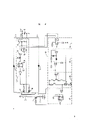
图3,是表示用于本实施例的拓扑结构的振铃机电路原理图;
图4,是包括了采用图3的拓扑结构的控制环路的振路铃机。
在图3中,示出了一个用于提供电流源I+和I-的反馈变流器,这些电流源受包括一对金属氧化物半导体场效应晶体管(MOSFET)7和8的次级开关级的控制。输出波形受两个电压反馈环路13和18的控制,使电路有两种工作方式。当需要足够幅度的振铃电流Iac时,内控制环路18将对初级电流进行调制以便维持输出波形的幅度。输出控制环路13将仅保持一对MOSFET 7和8中之一在输出波形的整个半周期内导通,从而提供合适的供电极性。
次级电流流过由MOSFET 7或8所选定的通路。这样就使输出电容器6被恰当地充电,从而产生所需要的输出波形。在需要大电流时不发生环流的电流,因而达到高效率、低功耗和低噪音。
当不需要、或仅需要很小的振铃机电流时,次级的MOSFET 7和8的工作状态从作为极性开关变为作为高频调制器。之所以有此需要,是因为当没有负载电流时输出电器6上的电压在每半个周期的后一半时间内没有放电通路,因而不能保持正弦输出波形的缘故。在这些轻负载情况下的过程中,环流的电流不是非常耗费的。
虽然本发明是参照一个反馈变流器进行描述的,但是可以采用各种替换的拓扑结构。
参看图4,其中外控制环路13包含一个分压器9,该分压器9用于监测电容器6上的输出电压电平。基准正弦波振荡器10的输出和分压器9的中间点都接到一个起比较器作用的差分放大器11。差分放大器11产生指示其两个输入之差的输出误差电压。该输出于是借助触发器12与一个时钟同步。这样就对任何一种状态给出等于5微秒的最小持续时间,而任何更长的持续时间都是该基本时间的倍乘值。
所得到的该外控制环路13的输出作为开关电压供到一对MOSFET 7和8的栅极上。这些MOSFET的电路结构使得当其中之一导通时另一就载止。这些MOSFET提供了一个通路,使得输出电容器6可按合适的极性充电。MOSFET7允许经过二极管4正向充电,MOSFET 8允许经过二极管5负向充电。所需要的充电电流由反馈变压器3提供,该变压器的次级绕组被联接而形成合适的通路。需要注意的是,变压器次级电感和输出电容器6构成一个低通滤波器,从而能够获得圆滑的输出电压波形。
当不需要、或仅需要很小的振铃机电流Iac时,输出电容器6上的电压没有维持正弦输出波形的外部放电通路。控制环路13将改变它的工作循环(duty cycle)以便保持电容器6上的正确的电压值。比较器11的两个输入容易维持平衡,因而出现空载状态。就这样,电容器在输出波形的半周期内存在多次充、放电,因而存在着环流电流。
送到差分放大器11的各输入也供到内控制环路18去。内控制环路18包含一个差分放大器14,该差分放大器14放大基准正弦波放大器10与分压器9中间点输出的差值信号。差分放大器14的输出再供到全波整流器15去,从该全波整流器15输出一个单极的误差电压。接着是一个压控电流源16,它起电平偏移作用,从而将一个误差电压Ve提供到脉宽调制器17去。
脉宽调制器17使初级的MOSFET 1导通,于是使反馈变压器3的初级电流增长。这个电流被电阻器2检测并用于使脉宽调制器17复位,从而提供电流工作方式控制。误差电压Ve的大小给定由脉宽调制器17供出的相应的脉冲宽度,因而限定初级的峰值电流。该初级电流于是通过变压器3的反馈作用变换到次级绕组去。
当要求振铃机电流Iac增加时,需要有较大的初级电流。这种电流增长是靠增加供到脉宽调制器17的误差电压Ve、并因而靠增加内控制环路18的输入信号间的整个差值而实现的,由于内控制环路18的这些输入信号也供到外控制环路13的比较器11去,使得在比较器11的两个输入端之间出现格外大的偏调。这种情况将使比较器11保持在一种状态,因而一对MOSFET 7和8中之一将在输出波形的完整的半周期内保持导通。当输出经过零值点而转变时,比较器11上的偏调改变极性并促使相反状态的一个MOSFET在下一个半周期内导通。
在这种工作方式下,输出开关级MOSFET 7和8仅仅是一个极性开关,输出幅度完全是由调制初级的内控制环路18而产生。这样就获得了高效率并因而在要求大振铃机电流时的损耗很低。
通过采用由两个电压反馈环路控制的反馈变流器拓扑结构,提供了一种具有两种工作方式的电路,这两种工作方式取决于需要的负载电流的大小。在需要大电流时,仅仅需要用一个高频开关级以便产生输出电压波形,使得电路具有高效率而相应地其电路装置的尺寸很小。
Claims (5)
1、一种用于电话系统的振铃机,包括一个变压器,其特征在于具有:
第一反馈环路,用于根据该振铃机输出控制所述变压器的初级电流;和
第二反馈环路,用于根据该振铃机输出控制所述变压器的次级电流。
2、如权利要求1的振铃机,其特征在于还包括:第一和第二反馈环路中的相应的差分放大器、一个跨接于该振铃机输出端的分压器、以及一个基准振荡器,该分压器和基准振荡器连接到每一个所述差分放大器的相应输入端上。
3、如权利要求1或2的振铃机,其特征在于,所述第一反馈环路包括一个脉宽调制器,该脉宽调制器连接到与所述变压器初级绕组串联的一个开关晶体管上。
4、如上述任一权利要求的振铃机,其特征在于,所述第二反馈环路的输出端连接到与所述变压器次级绕组串联的一个开关晶体管上。
5、如上述任一权利要求的振铃机,其特征在于,具有反馈拓扑结构。
Applications Claiming Priority (2)
| Application Number | Priority Date | Filing Date | Title |
|---|---|---|---|
| GB9026504.2 | 1990-12-05 | ||
| GB909026504A GB9026504D0 (en) | 1990-12-05 | 1990-12-05 | Telephone ringer circuit |
Publications (1)
| Publication Number | Publication Date |
|---|---|
| CN1062061A true CN1062061A (zh) | 1992-06-17 |
Family
ID=10686559
Family Applications (1)
| Application Number | Title | Priority Date | Filing Date |
|---|---|---|---|
| CN91111571A Pending CN1062061A (zh) | 1990-12-05 | 1991-12-05 | 电话振铃机电路 |
Country Status (10)
| Country | Link |
|---|---|
| EP (1) | EP0489512A3 (zh) |
| JP (1) | JPH04340841A (zh) |
| KR (1) | KR920013934A (zh) |
| CN (1) | CN1062061A (zh) |
| AU (1) | AU651398B2 (zh) |
| CA (1) | CA2056132A1 (zh) |
| FI (1) | FI915711A7 (zh) |
| GB (2) | GB9026504D0 (zh) |
| IE (1) | IE914004A1 (zh) |
| PT (1) | PT99681A (zh) |
Families Citing this family (3)
| Publication number | Priority date | Publication date | Assignee | Title |
|---|---|---|---|---|
| DE4218845C2 (de) * | 1992-06-09 | 1994-10-27 | Bosch Telecom | Schaltungsanordnung für einen Rufspannungsgenerator |
| DE19740137A1 (de) * | 1997-09-12 | 1999-03-18 | Alsthom Cge Alcatel | Verfahren und Schaltungsanordnung zur Rufwechselspannungserzeugung für elektronische Teilnehmerschaltungen |
| US6252787B1 (en) | 2000-05-12 | 2001-06-26 | Honeywell International Inc. | Controllable circuit for providing bi-directional current to a load |
Family Cites Families (2)
| Publication number | Priority date | Publication date | Assignee | Title |
|---|---|---|---|---|
| GB8606151D0 (en) * | 1986-03-12 | 1986-04-16 | Gen Electric Co Plc | Telephone system circuit |
| US4890210A (en) * | 1988-11-15 | 1989-12-26 | Gilbarco, Inc. | Power supply having combined forward converter and flyback action for high efficiency conversion from low to high voltage |
-
1990
- 1990-12-05 GB GB909026504A patent/GB9026504D0/en active Pending
-
1991
- 1991-11-15 EP EP19910310581 patent/EP0489512A3/en not_active Withdrawn
- 1991-11-15 GB GB9124299A patent/GB2250663B/en not_active Expired - Lifetime
- 1991-11-18 IE IE400491A patent/IE914004A1/en not_active Application Discontinuation
- 1991-11-26 CA CA002056132A patent/CA2056132A1/en not_active Abandoned
- 1991-12-02 JP JP3343888A patent/JPH04340841A/ja active Pending
- 1991-12-04 FI FI915711A patent/FI915711A7/fi not_active Application Discontinuation
- 1991-12-04 AU AU88854/91A patent/AU651398B2/en not_active Ceased
- 1991-12-04 PT PT99681A patent/PT99681A/pt not_active Application Discontinuation
- 1991-12-04 KR KR1019910022137A patent/KR920013934A/ko not_active Withdrawn
- 1991-12-05 CN CN91111571A patent/CN1062061A/zh active Pending
Also Published As
| Publication number | Publication date |
|---|---|
| FI915711L (fi) | 1992-06-06 |
| AU651398B2 (en) | 1994-07-21 |
| FI915711A7 (fi) | 1992-06-06 |
| PT99681A (pt) | 1994-01-31 |
| EP0489512A3 (en) | 1993-03-24 |
| EP0489512A2 (en) | 1992-06-10 |
| AU8885491A (en) | 1992-06-11 |
| GB2250663A (en) | 1992-06-10 |
| FI915711A0 (fi) | 1991-12-04 |
| GB9124299D0 (en) | 1992-01-08 |
| GB9026504D0 (en) | 1991-01-23 |
| KR920013934A (ko) | 1992-07-30 |
| GB2250663B (en) | 1995-04-19 |
| IE914004A1 (en) | 1992-06-17 |
| JPH04340841A (ja) | 1992-11-27 |
| CA2056132A1 (en) | 1992-06-06 |
Similar Documents
| Publication | Publication Date | Title |
|---|---|---|
| CN100541995C (zh) | 功率因数改善电路 | |
| US6034513A (en) | System and method for controlling power factor and power converter employing the same | |
| EP0553179B1 (en) | Dc/ac converter | |
| US7279868B2 (en) | Power factor correction circuits | |
| Lai et al. | A general constant-frequency pulsewidth modulator and its applications | |
| WO1996007960A1 (en) | A synchronous switching cascade connected offline pfc-pwm combination power converter controller | |
| US20230299660A1 (en) | Switching sequence controlled current steering for stacked half bridge converters | |
| CN107612326A (zh) | 一种双向级联式Buck‑Boost变换器的软开关调制方法 | |
| CN115534715B (zh) | 一种可配置充电电压和充电电流的恒流恒压ipt系统 | |
| Redl et al. | Small-signal dynamic analysis of regulated class-E dc/dc converters | |
| CN107026568A (zh) | 控制电路、控制方法及开关电源 | |
| CN118316326A (zh) | 一种辅助电感双降压半桥功率放大器的电流解耦控制方法 | |
| CN201750341U (zh) | 输出电压可调的射频电源 | |
| US8760230B2 (en) | Switching amplifier with pulsed current source and sink | |
| US9602067B2 (en) | Switching amplifier with pulsed current supply | |
| CN1062061A (zh) | 电话振铃机电路 | |
| CN106655840B (zh) | 降低平均开关速率的三相电流型pwm整流器控制方法 | |
| CN104640268A (zh) | 一种高功率因数恒流控制电路及led照明设备 | |
| CN119010560A (zh) | 一种四管Buck-Boost PFC变换器控制方法和控制电路 | |
| CN118117880A (zh) | 一种新型准单级变换器 | |
| EP4718704A1 (en) | Rectifier with inherent unity power factor | |
| KR100292489B1 (ko) | 소프트 스위칭 기술을 이용한 역률제어용 승압형 컨버터 | |
| Li et al. | A pulse density modulation method for ZVS full-bridge converters in wireless power transfer systems | |
| CN114337327B (zh) | 功率解耦电路、电源以及电子设备 | |
| Ting et al. | A soft switching power factor correction interleaved AC-DC boost converter |
Legal Events
| Date | Code | Title | Description |
|---|---|---|---|
| C06 | Publication | ||
| PB01 | Publication | ||
| C01 | Deemed withdrawal of patent application (patent law 1993) | ||
| WD01 | Invention patent application deemed withdrawn after publication |