CN1114948C - Semiconductor chip package having combined structure of lead-on-chip leads and standard normal leads - Google Patents
Semiconductor chip package having combined structure of lead-on-chip leads and standard normal leads Download PDFInfo
- Publication number
- CN1114948C CN1114948C CN97121615A CN97121615A CN1114948C CN 1114948 C CN1114948 C CN 1114948C CN 97121615 A CN97121615 A CN 97121615A CN 97121615 A CN97121615 A CN 97121615A CN 1114948 C CN1114948 C CN 1114948C
- Authority
- CN
- China
- Prior art keywords
- lead
- semiconductor chip
- die package
- electrode pad
- active surface
- Prior art date
- Legal status (The legal status is an assumption and is not a legal conclusion. Google has not performed a legal analysis and makes no representation as to the accuracy of the status listed.)
- Expired - Fee Related
Links
Images


Classifications
-
- H—ELECTRICITY
- H10—SEMICONDUCTOR DEVICES; ELECTRIC SOLID-STATE DEVICES NOT OTHERWISE PROVIDED FOR
- H10W—GENERIC PACKAGES, INTERCONNECTIONS, CONNECTORS OR OTHER CONSTRUCTIONAL DETAILS OF DEVICES COVERED BY CLASS H10
- H10W70/00—Package substrates; Interposers; Redistribution layers [RDL]
- H10W70/40—Leadframes
- H10W70/411—Chip-supporting parts, e.g. die pads
- H10W70/415—Leadframe inner leads serving as die pads
-
- H—ELECTRICITY
- H10—SEMICONDUCTOR DEVICES; ELECTRIC SOLID-STATE DEVICES NOT OTHERWISE PROVIDED FOR
- H10W—GENERIC PACKAGES, INTERCONNECTIONS, CONNECTORS OR OTHER CONSTRUCTIONAL DETAILS OF DEVICES COVERED BY CLASS H10
- H10W70/00—Package substrates; Interposers; Redistribution layers [RDL]
- H10W70/40—Leadframes
-
- H—ELECTRICITY
- H10—SEMICONDUCTOR DEVICES; ELECTRIC SOLID-STATE DEVICES NOT OTHERWISE PROVIDED FOR
- H10W—GENERIC PACKAGES, INTERCONNECTIONS, CONNECTORS OR OTHER CONSTRUCTIONAL DETAILS OF DEVICES COVERED BY CLASS H10
- H10W72/00—Interconnections or connectors in packages
- H10W72/50—Bond wires
- H10W72/541—Dispositions of bond wires
- H10W72/5449—Dispositions of bond wires not being orthogonal to a side surface of the chip, e.g. fan-out arrangements
-
- H—ELECTRICITY
- H10—SEMICONDUCTOR DEVICES; ELECTRIC SOLID-STATE DEVICES NOT OTHERWISE PROVIDED FOR
- H10W—GENERIC PACKAGES, INTERCONNECTIONS, CONNECTORS OR OTHER CONSTRUCTIONAL DETAILS OF DEVICES COVERED BY CLASS H10
- H10W72/00—Interconnections or connectors in packages
- H10W72/50—Bond wires
- H10W72/551—Materials of bond wires
- H10W72/552—Materials of bond wires comprising metals or metalloids, e.g. silver
- H10W72/5522—Materials of bond wires comprising metals or metalloids, e.g. silver comprising gold [Au]
-
- H—ELECTRICITY
- H10—SEMICONDUCTOR DEVICES; ELECTRIC SOLID-STATE DEVICES NOT OTHERWISE PROVIDED FOR
- H10W—GENERIC PACKAGES, INTERCONNECTIONS, CONNECTORS OR OTHER CONSTRUCTIONAL DETAILS OF DEVICES COVERED BY CLASS H10
- H10W72/00—Interconnections or connectors in packages
- H10W72/50—Bond wires
- H10W72/551—Materials of bond wires
- H10W72/552—Materials of bond wires comprising metals or metalloids, e.g. silver
- H10W72/5524—Materials of bond wires comprising metals or metalloids, e.g. silver comprising aluminium [Al]
-
- H—ELECTRICITY
- H10—SEMICONDUCTOR DEVICES; ELECTRIC SOLID-STATE DEVICES NOT OTHERWISE PROVIDED FOR
- H10W—GENERIC PACKAGES, INTERCONNECTIONS, CONNECTORS OR OTHER CONSTRUCTIONAL DETAILS OF DEVICES COVERED BY CLASS H10
- H10W72/00—Interconnections or connectors in packages
- H10W72/50—Bond wires
- H10W72/551—Materials of bond wires
- H10W72/552—Materials of bond wires comprising metals or metalloids, e.g. silver
- H10W72/5525—Materials of bond wires comprising metals or metalloids, e.g. silver comprising copper [Cu]
-
- H—ELECTRICITY
- H10—SEMICONDUCTOR DEVICES; ELECTRIC SOLID-STATE DEVICES NOT OTHERWISE PROVIDED FOR
- H10W—GENERIC PACKAGES, INTERCONNECTIONS, CONNECTORS OR OTHER CONSTRUCTIONAL DETAILS OF DEVICES COVERED BY CLASS H10
- H10W72/00—Interconnections or connectors in packages
- H10W72/50—Bond wires
- H10W72/59—Bond pads specially adapted therefor
-
- H—ELECTRICITY
- H10—SEMICONDUCTOR DEVICES; ELECTRIC SOLID-STATE DEVICES NOT OTHERWISE PROVIDED FOR
- H10W—GENERIC PACKAGES, INTERCONNECTIONS, CONNECTORS OR OTHER CONSTRUCTIONAL DETAILS OF DEVICES COVERED BY CLASS H10
- H10W72/00—Interconnections or connectors in packages
- H10W72/851—Dispositions of multiple connectors or interconnections
- H10W72/853—On the same surface
- H10W72/865—Die-attach connectors and bond wires
-
- H—ELECTRICITY
- H10—SEMICONDUCTOR DEVICES; ELECTRIC SOLID-STATE DEVICES NOT OTHERWISE PROVIDED FOR
- H10W—GENERIC PACKAGES, INTERCONNECTIONS, CONNECTORS OR OTHER CONSTRUCTIONAL DETAILS OF DEVICES COVERED BY CLASS H10
- H10W72/00—Interconnections or connectors in packages
- H10W72/90—Bond pads, in general
- H10W72/931—Shapes of bond pads
- H10W72/932—Plan-view shape, i.e. in top view
-
- H—ELECTRICITY
- H10—SEMICONDUCTOR DEVICES; ELECTRIC SOLID-STATE DEVICES NOT OTHERWISE PROVIDED FOR
- H10W—GENERIC PACKAGES, INTERCONNECTIONS, CONNECTORS OR OTHER CONSTRUCTIONAL DETAILS OF DEVICES COVERED BY CLASS H10
- H10W72/00—Interconnections or connectors in packages
- H10W72/90—Bond pads, in general
- H10W72/941—Dispositions of bond pads
- H10W72/944—Dispositions of multiple bond pads
- H10W72/9445—Top-view layouts, e.g. mirror arrays
-
- H—ELECTRICITY
- H10—SEMICONDUCTOR DEVICES; ELECTRIC SOLID-STATE DEVICES NOT OTHERWISE PROVIDED FOR
- H10W—GENERIC PACKAGES, INTERCONNECTIONS, CONNECTORS OR OTHER CONSTRUCTIONAL DETAILS OF DEVICES COVERED BY CLASS H10
- H10W72/00—Interconnections or connectors in packages
- H10W72/90—Bond pads, in general
- H10W72/951—Materials of bond pads
- H10W72/952—Materials of bond pads comprising metals or metalloids, e.g. PbSn, Ag or Cu
-
- H—ELECTRICITY
- H10—SEMICONDUCTOR DEVICES; ELECTRIC SOLID-STATE DEVICES NOT OTHERWISE PROVIDED FOR
- H10W—GENERIC PACKAGES, INTERCONNECTIONS, CONNECTORS OR OTHER CONSTRUCTIONAL DETAILS OF DEVICES COVERED BY CLASS H10
- H10W74/00—Encapsulations, e.g. protective coatings
-
- H—ELECTRICITY
- H10—SEMICONDUCTOR DEVICES; ELECTRIC SOLID-STATE DEVICES NOT OTHERWISE PROVIDED FOR
- H10W—GENERIC PACKAGES, INTERCONNECTIONS, CONNECTORS OR OTHER CONSTRUCTIONAL DETAILS OF DEVICES COVERED BY CLASS H10
- H10W90/00—Package configurations
- H10W90/701—Package configurations characterised by the relative positions of pads or connectors relative to package parts
- H10W90/731—Package configurations characterised by the relative positions of pads or connectors relative to package parts of die-attach connectors
- H10W90/736—Package configurations characterised by the relative positions of pads or connectors relative to package parts of die-attach connectors between a chip and a stacked lead frame, conducting package substrate or heat sink
-
- H—ELECTRICITY
- H10—SEMICONDUCTOR DEVICES; ELECTRIC SOLID-STATE DEVICES NOT OTHERWISE PROVIDED FOR
- H10W—GENERIC PACKAGES, INTERCONNECTIONS, CONNECTORS OR OTHER CONSTRUCTIONAL DETAILS OF DEVICES COVERED BY CLASS H10
- H10W90/00—Package configurations
- H10W90/701—Package configurations characterised by the relative positions of pads or connectors relative to package parts
- H10W90/751—Package configurations characterised by the relative positions of pads or connectors relative to package parts of bond wires
- H10W90/756—Package configurations characterised by the relative positions of pads or connectors relative to package parts of bond wires between a chip and a stacked lead frame, conducting package substrate or heat sink
Landscapes
- Lead Frames For Integrated Circuits (AREA)
- Wire Bonding (AREA)
Abstract
一种半导体芯片封装,包括位于集成电路(IC)的有源表面上的中央电极焊盘和周边电极焊盘。该封装还包括引线框,引线框具有:第一内引线,其直接贴装至有源表面并且连接至中央电极焊盘;第二内引线,它远离该芯片并连接至周边电极焊盘;第一外引线,连接至第一内引线;以及第二外引线,连接至第二内引线。沿着芯片的长边或是沿着IC的短边,通过布置第二外引线可形成双列类型的或者是四边形的封装。
A semiconductor chip package includes a central electrode pad and peripheral electrode pads on an active surface of an integrated circuit (IC). The package also includes a lead frame having: a first inner lead mounted directly to the active surface and connected to a central electrode pad; a second inner lead away from the chip and connected to a peripheral electrode pad; an outer lead connected to the first inner lead; and a second outer lead connected to the second inner lead. A dual row type or a quadrilateral package can be formed by arranging the second outer leads along the long side of the chip or along the short side of the IC.
Description
技术领域technical field
本发明一般地涉及半导体芯片封装,尤其是涉及在高密度的半导体芯片中布置接触引线的方法。The present invention relates generally to semiconductor chip packaging, and more particularly to methods of arranging contact leads in high density semiconductor chips.
背景技术Background technique
一般地,半导体芯片在其有源表面具有多个电极焊盘以便于集成电路元件和外部之间连接电信号。依赖于电极焊盘的排列,半导体芯片可以被分为中央焊盘型器件及周边焊盘型器件,其中在中央焊盘型器件中电极焊盘分布在芯片有源表面的中央区域,在周边焊盘型器件中电极焊盘则沿着芯片有源表面的边缘而布置。中央焊盘器件显示出小的信号偏差,因为缩短的总线线路而有很高的信号传输速度,以及在电极焊盘的设计方面较为简单且相对容易。进而,按照中央焊盘设计生产的半导体存储器芯片的尺寸比周边存储器芯片的尺寸小大约4%至7%,其结果使得单个晶片上放置的净焊盘的数目增加并因此提高了生产量。由于这些以及其它的优点,目前存储器器件的制造商们广泛采用中央焊盘型芯片。Generally, a semiconductor chip has a plurality of electrode pads on its active surface to facilitate connection of electrical signals between integrated circuit elements and the outside. Depending on the arrangement of the electrode pads, semiconductor chips can be divided into central pad type devices and peripheral pad type devices, wherein in the central pad type devices, the electrode pads are distributed in the central area of the active surface of the chip, and in the peripheral pad type devices. In pad-type devices, the electrode pads are arranged along the edge of the active surface of the chip. Central pad devices exhibit small signal deviations, high signal transmission speeds due to shortened bus lines, and are simple and relatively easy in terms of electrode pad design. Furthermore, semiconductor memory chips produced with a central pad design are approximately 4% to 7% smaller in size than peripheral memory chips, resulting in an increased number of net pads placed on a single wafer and thus increased throughput. Because of these and other advantages, center pad type chips are now widely used by manufacturers of memory devices.
为了封装中央焊盘型器件,无论是芯片上引线(LOC)的设计方案,或是长引线键合方案都可以采用,其中芯片上引线是引线直接贴装至芯片的有源表面,长引线键合是引线离芯片边缘很远并且是通过长键合线与电极焊盘相连接。但是,由于有这样长的键合线,后者有一些问题比如较差的可靠性。另一方面,尽管LOC引线比标准常规引线需要更多的制造成本,但键合线能够制作的更短些并因此能提高封装的可靠性,进而,LOC封装能提高芯片的尺寸对总的封装的比率。In order to package central pad type devices, either lead-on-chip (LOC) design schemes or long-wire bonding schemes can be used, wherein the leads on the chip are directly attached to the active surface of the chip, and the long-lead bond The combination is that the leads are far away from the edge of the chip and are connected to the electrode pads through long bonding wires. However, the latter has some problems such as poor reliability due to such long bonding wires. On the other hand, although LOC wires require more manufacturing cost than standard conventional wires, the bonding wires can be made shorter and thus improve the reliability of the package. In turn, the LOC package can increase the size of the chip to the total package. The ratio.
尽管如此,由于存储器芯片的密度不断地增大,封装工程师面临着一些技术问题,那就是,因为引线框的制造技术跟不上芯片的缩小率,将所有的LOC引线布置在下一代存储器芯片的缩小的有源表面上是不可能的。一般地,引线框引线或者用冲压或者用光腐蚀的方式来构图。在这两种方法中,仅仅当引线的宽度或者相邻引线之间的距离等于或大于该引线框的厚度的80%的时候,才能制作成理想的引线图形。为了克服这种局限性,可以考虑减小引线框的厚度,但是,这种设计方案并不理想,因为在装配过程中,薄的引线框极易损坏并且这种构图的引线很容易被损坏,甚至是由于一次小小的冲击。Nevertheless, due to the ever-increasing density of memory chips, packaging engineers are faced with some technical problems, that is, because the manufacturing technology of the lead frame cannot keep up with the shrinking ratio of the chip, all the LOC leads are placed on the next generation memory chip. Shrinking the active surface is not possible. Typically, leadframe leads are patterned either by stamping or by photoetching. In these two methods, only when the width of the lead or the distance between adjacent leads is equal to or greater than 80% of the thickness of the lead frame, can an ideal lead pattern be produced. In order to overcome this limitation, reducing the thickness of the lead frame can be considered, however, this design scheme is not ideal, because the thin lead frame is extremely fragile and the leads of this pattern are easily damaged during the assembly process, Even due to a small shock.
因此,有必要在并不丢失中央焊盘结构和LOC引线结构的优点的条件下来封装高密度半导体芯片。Therefore, it is necessary to package high-density semiconductor chips without losing the advantages of the central pad structure and the LOC lead structure.
发明内容Contents of the invention
本发明的目的是提供一种半导体芯片封装,它能通过使用中央焊盘结构及LOC引线结构来装配高密度半导体芯片。An object of the present invention is to provide a semiconductor chip package capable of mounting high-density semiconductor chips by using a center pad structure and an LOC lead structure.
本发明的另一目的是提供一种半导体芯片封装,它能够克服引线框的生产的局限并能有效地封装高密度半导体芯片。Another object of the present invention is to provide a semiconductor chip package capable of overcoming the limitations of lead frame production and efficiently packaging high-density semiconductor chips.
在依据本发明的半导体芯片封装中,半导体芯片具有中央焊盘的组合型结合,引线框提供有多个第一内引线,它们直接贴装至芯片的有源表面并且电连接至中央电极焊盘;以及多个第二内引线,它们远离芯片的边缘而分布并且电连接至周边电极焊盘。In the semiconductor chip package according to the present invention, the semiconductor chip has a combination type bonding of the central pad, and the lead frame is provided with a plurality of first inner leads which are directly mounted to the active surface of the chip and electrically connected to the central electrode pad and a plurality of second inner leads distributed away from the edge of the chip and electrically connected to the peripheral electrode pads.
一般地,半导体芯片呈矩形,具有一长边和一短边,当引线框的外引线与内引线制作成一体,并且既沿着长边又沿着短边而分布时,就可得到一个四边形的封装器件,而且如果外引线沿着芯片的长边而分布时,即得到双列类型的封装器件。Generally, a semiconductor chip is rectangular with a long side and a short side. When the outer lead and the inner lead of the lead frame are integrated and distributed along both the long side and the short side, a quadrilateral shape can be obtained. packaged device, and if the outer leads are distributed along the long side of the chip, a dual row type packaged device is obtained.
应用于本发明的封装的引线框包括连杆,它连接于角部引线和引线框的侧轨之间,以便在装配过程中单个封装能够保持成条形直至它们成为单一体,并且最长的角部引线能够被支持和保护以免损坏。引线框可能还包括对准键以便当芯片贴装至引线框的引线且当引线与电极焊盘电连接的时候,来提高引线框与半导体芯片的可识别性和精确的布置。The lead frame applied to the package of the present invention includes tie bars that connect between the corner leads and the side rails of the lead frame so that the individual packages can be held in strips during assembly until they become a single body, and the longest The corner leads can be supported and protected from damage. The lead frame may further include alignment keys to improve recognizability and accurate placement of the lead frame and semiconductor chip when the chip is attached to the leads of the lead frame and when the leads are electrically connected to the electrode pads.
LOC结构的第一内引线具有倾斜区域(up-set,regions),该倾斜区域的大小由芯片的厚度及用来将芯片贴装至第一引线的粘合剂的厚度来确定,通过控制该倾斜区域的大小,即有可能获得该封装器件的最佳的垂直结构。The first inner lead of the LOC structure has an up-set region, the size of which is determined by the thickness of the chip and the thickness of the adhesive used to attach the chip to the first lead, by controlling the Depending on the size of the inclined area, it is possible to obtain the best vertical structure of the packaged device.
附图说明 Description of drawings
上面已经叙述了本发明的一些目的和优点,通过下文的详细说明,并且参照附图,将能更加充分地理解其它的目的和优点,其中:Some objects and advantages of the present invention have been described above, through the following detailed description, and with reference to the accompanying drawings, other objects and advantages will be more fully understood, wherein:
图1是本发明的优选的引线框条的局部平面图;Figure 1 is a partial plan view of a preferred leadframe strip of the present invention;
图2是根据本发明的一个实施例的半导体芯片封装的平面图;2 is a plan view of a semiconductor chip package according to one embodiment of the present invention;
图3是根据本发明的半导体芯片封装的局部平面图;3 is a partial plan view of a semiconductor chip package according to the present invention;
图4A是沿图2中线IV-A所取的截面图;Fig. 4A is a sectional view taken along line IV-A in Fig. 2;
图4B是沿图2中线IV-B所取的截面图;Fig. 4B is a sectional view taken along line IV-B in Fig. 2;
图5是根据本发明的另一实施例的半导体芯片封装的截面图;5 is a cross-sectional view of a semiconductor chip package according to another embodiment of the present invention;
图6是本发明的示例性半导体芯片封装的透视图;6 is a perspective view of an exemplary semiconductor chip package of the present invention;
图7是根据本发明的再一个实施例的半导体芯片封装的局部平面图;及7 is a partial plan view of a semiconductor chip package according to yet another embodiment of the present invention; and
图8是根据本发明的再一个实施例的半导体芯片封装的透视图。FIG. 8 is a perspective view of a semiconductor chip package according to yet another embodiment of the present invention.
具体实施方式Detailed ways
现在,参照附图,详细地阐述本发明的实施例。Embodiments of the present invention will now be described in detail with reference to the drawings.
图1是本发明的优选引线框条的局部平面图,引线框条100具有若干个相同的引线框图形,因而能使管芯键合,导线键合,以及模塑工艺应用至多个芯片。在装配过程中,通过使用输送孔16,引线框条100被输送,这些重复的单个引线框图形由槽22隔开,为简单起见,图1中仅仅示出了一个单个引线框图形。1 is a partial plan view of a preferred leadframe strip of the present invention.
每个单个图形都有多个内引线10和12,它们电连接至半导体芯片(未示出)的电极焊盘,以及多个外引线14a和14b,用于电连接芯片,内引线与外引线通过阻拦条28相耦连,当塑料模制树脂满了模塑区域34以形成一封装保护体时,阻拦条28将会防止模塑树脂的溢出。在模塑过程之后,阻拦条28和连杆18被切掉,这样内引线和外引线即成独立状态。Each single pattern has a plurality of
借助于侧轨24,各单个引线框图形被制作成为条带形,通过连杆18位于模塑区域34的四个角部的角部引线15连接至侧轨24上,当阻拦条28被切掉可是单个引线框并未最后成为单一体时,连接角部引线15和侧轨24的连杆18用于支撑单个引线框,而且,连杆18能够防止角部引线15的任何可能的变形,角部引线15具有最长的长度因而在装配过程中容易损坏变形。By means of the
引线20这样称呼并不是连接引线,它们并不连接到芯片上,电源引线26是施加至芯片上的正电源电压VDD和负电源电压VSS的通道,电源引线26被分成两个部分以便能减少引线的电感。The
对于引线框引线,第一内引线10是LOC引线,而第二内引线是标准常规引线。通过一粘合材料32第一内引线10直接贴装至芯片的有源表面,并且它有一弯曲区域(倾斜区域)30,这种组合引线结构适合于封装具有中央分布的电极焊盘及周边分布的电极焊盘的半导体芯片。For leadframe leads, the first
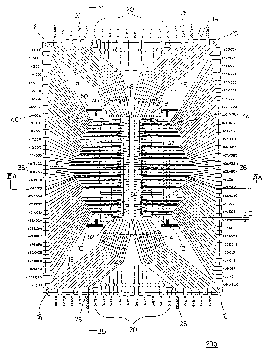
图2是根据本发明的一个实施例的半导体芯片封装的平面图,在图2中,半导体芯片封装200具有总共一百个输入/输出管脚,其中的每一个发送和接收不同的信号。FIG. 2 is a plan view of a semiconductor chip package according to one embodiment of the present invention. In FIG. 2, the
半导体芯片40具有一长边42和一短边44,在半导体存储器芯片中这种矩形结构是很普遍的。在半导体芯片40的有源表面46上面,许多内部电路元件比如存储器单元,控制栅极,金属线,和多个电极焊盘48和49被形成,电极焊盘包括中央电极焊盘48和周边电极焊盘49,其中电极焊盘48位于芯片有源表面46的中央区域上面按两行并且平行于长边42而排列着,电极焊盘49则在芯片有源表面46的边缘附近沿着短边44而分布。
第一LOC内引线10沿着芯片的长边42排列着并且通过粘合剂32直接贴装至芯片的有源表面46,由键合线52该第一内引线10电连接至中央电极焊盘48,且电连接至第一外引线14a,外引线14a同样也是沿着长边42分布。The first LOC
粘合剂32是电绝缘的,并且可以是由聚酰亚胺制成的双面粘合剂,或者是使用胶带或者是淀积部分固化的粘合剂,半导体芯片能粘结到第一内引线上。前一种情况,胶带粘合到第一内引线上,然后该第一内引线与芯片的有源表面相对准并布置在其上。在高温下通过对第一内引线与芯片加压,二者便键合在一起。同时,在芯片的有源表面上通过淀积部分固化的液体粘合材料,然后在高温下通过对第一内引线和芯片加压,即可进行管芯键合操作。
第二内引线12沿着半导体芯片的短边44排列并且具有标准常规结构,也就是,它们远离芯片的边缘。通过键合线52第二内引线12电连接至周边电极焊盘49,并且与第二外引线14b相连接,引线14b沿着芯片的短边44而分布。The second inner leads 12 are arranged along the
对于这种LOC引线和标准引线的组合结构,有可能克服引线框的加工过程的局限性,因而能有效地封装高密度存储器件,另外,由于半导体芯片除了周边电极焊盘之外还具有中央电极焊盘,因而同样能获得中央类型的优点,比如小信号偏差,很高的信号传输速率以及在电极焊盘的设计方面较为简单且相对容易。For this combined structure of LOC leads and standard leads, it is possible to overcome the limitation of the processing process of the lead frame, so that high-density memory devices can be packaged effectively. The advantages of the central type, such as small signal deviation, high signal transmission rate, and simplicity and relative ease in the design of the electrode pads can thus also be obtained.
如图2所示,周边电极焊盘49与粘合剂32必须相隔一距离D,距离D是考虑了若干个参数后确定的,这些参数比如是引线框的加工公差,封装过程中的加工公差,以及该第一内引线与用于线键合的毛细管之间的接触情况,较为可取的是,将距离D保持在等于或者大于20密耳的状态。As shown in FIG. 2, the
脚号为36-45和86-96的虚设引线20并不是连接引线,它们是由于比如是按照JEDEC所定义的外引线的数目规格与为了某一存储器件的功能的外引线的真实数目之间差异而产生的。The dummy leads 20 whose pin numbers are 36-45 and 86-96 are not connection leads, they are due to, for example, the difference between the number specification of the outer leads defined by JEDEC and the real number of outer leads for the function of a certain memory device. resulting from differences.
第一内引线10可能包括对准键50,在管芯键合过程以及线键合过程中它用来帮助识别引线框引线和存储器芯片40的位置。或者是经过蚀刻或者是通过冲压的方法,对准键50能够与引线框图形同时制作成,而且很自然地由和引线框条相同的材料构成。The first
电源引线26为存储器芯片40提供电源电压比如VDD和VSS,并且使其端部分成两个部分,这两个平行的电源通道使得引线框引线之间的电感减少,因而能够提供相对较稳定的电源。The
对于这种稳定的电源,可以采用如图3所示的总线结构。参照图3,总线汇流条56连接着一些内引线并形成一个单通道,恒定的电源电压通过这些内引线被施加上。因此,电源电压的恒定电平能够被施加到不同的电路元件上,并且电源的噪声效果能被减少,图3中,具有管脚号5,11和19的内引线由总线汇流条56a连接以便用于接收负的VSS电源电压信号,而管脚号为59,67,73和79的内引线由总线汇流条56b来连接,其中正的VDD电源电压信号施加至总线汇流条56b上。For this stable power supply, the bus structure shown in Figure 3 can be used. Referring to FIG. 3, the bus bar 56 connects inner leads and forms a single channel through which a constant power supply voltage is applied. Therefore, a constant level of power supply voltage can be applied to different circuit elements, and the noise effect of the power supply can be reduced. In FIG. It is used to receive negative VSS power supply voltage signal, and the inner leads with pin numbers 59, 67, 73 and 79 are connected by bus bus bar 56b, wherein the positive VDD power supply voltage signal is applied to bus bus bar 56b.
如图2所示,当第一内引线10贴装至芯片的有源表面46上时,第一内引线必须分布成不置于保险盒54之上。保险盒54一般提供用来以多余的单元来替换有故障的存储器件的存储单元,并且具有外露金属线,例如是铝线,它能被激光切断。如果保险盒54被第一内引线所覆盖,则修复故障的存储器单元将变得不可能。As shown in FIG. 2 , when the first inner leads 10 are mounted on the
如图4A所示,第一内引线10具有倾斜区域30,图4A是沿图2中线IVA所取的截面图。倾斜区域30将半导体芯片40放置在保护性的封装体60的中央部位。例如,如果半导体芯片具有197密耳×340密耳的尺寸和0.3密耳的厚度,并且粘合剂的厚度t是0.1密耳,则该倾斜区域30的尺寸可以是大约0.2密耳以便使从半导体芯片到封装体的顶面的距离d1是1.05密耳,基本上等于从半导体芯片至封装体的底面的距离d2。保护性封装体是经过模塑过程而形成的,其中液态模制树脂以高压力注入至凹腔中,引线框条放置在该凹腔中,此时,如果距离d1和d2不一样,则该模制树脂的注射力在该封装体的上部和下部是不均衡的,并且因而可能发生半导体芯片的倾斜,这种芯片倾斜在随后的装配过程中会引起封装体的曲翘,但是,在本发明中,由于封装体的上部以及下部的平衡能够通过控制倾斜区域30的大小来调节,倾斜区域30形成于第一内引线10中,这样即能获得最佳的封装体的垂直结构,尽管倾斜区域30的大小被描述为大约0.2密耳,本领域的那些普通的技术人员会懂得,根据半导体芯片的厚度以及粘合剂的厚度该尺寸是可以变化的。As shown in FIG. 4A , the first
图4B是沿图2中线IVB所取的截面图,如前面所说明的,周边电极焊盘49沿着半导体芯片40的短边排列,并且通过键合线52电连接至第二内引线12。该第二内引线12是标准常规引线,它们离开半导体芯片40而排列。4B is a cross-sectional view taken along line IVB in FIG. The second inner leads 12 are standard conventional leads which are arranged away from the
如图2和4B所示,半导体芯片封装200具有内引线10和12,通过键合线52它们电连接至电极焊盘48和49,但是,该直接贴装至芯片有源表面46上的第一内引线10通过使用金属凸点而不是键合线亦能电连接至中央电极焊盘48。As shown in FIGS. 2 and 4B, the
图5是根据本发明的一实施例的半导体芯片封装的截面图,参照图5,半导体芯片封装210的第一内引线10贴装至半导体芯片40的有源表面,并且通过金属凸点70电连接至中央电极焊盘48,该金属凸点70形成于电极焊盘48的上面,金属凸点70可以是金凸点,铜凸点或者是锡-铅凸点,金属凸点70与第一内引线10通过热-压方法键合,此时,必须注意该引线与电极焊盘的精确对准度。尽管图5中未示出,为了提高第一内引线10与半导体芯片40之间的键合力,会使用粘合剂。5 is a cross-sectional view of a semiconductor chip package according to an embodiment of the present invention. Referring to FIG. Connected to the
图6是根据本发明的另一实施例的半导体芯片封装的透视图。半导体芯片封装300是一个四边形封装,其中外引线14沿着封装体60的四个边伸出,外引线14形状为一鸥翼状或是一J型引线以便封装300能够表面安装至电路板(未示出)上面。四边形封装适合于具有许多输入/输出管脚的芯片,并且比起管脚-插入类型的封装它代表着一种提高的封装密度。FIG. 6 is a perspective view of a semiconductor chip package according to another embodiment of the present invention. The semiconductor chip package 300 is a quadrilateral package, wherein the outer leads 14 protrude along the four sides of the
通过沿着半导体芯片40的长边42排列该第一外引线14a以及沿着芯片40的短边44设置该第二外引线14b,即能获得这种四边形的封装器件,如图1和2所示。By arranging the first
图7是根据本发明的再一实施例的半导体芯片封装的平面图,类似于图2中所示的实施例,图7中所示的半导体芯片封装400包括LOC结构的第一内引线110,它们直接贴装至芯片的有源表面146上并且电连接至中央电极焊盘149,该封装还包括标准第二内引线112,它们离开半导体芯片140的短边144分布,并且电连接至周边电极焊盘149。7 is a plan view of a semiconductor chip package according to another embodiment of the present invention, similar to the embodiment shown in FIG. 2, the semiconductor chip package 400 shown in FIG. 7 includes a first inner lead 110 of a LOC structure, and Mounted directly on the active surface 146 of the chip and electrically connected to the central electrode pad 149, the package also includes standard second inner leads 112 distributed away from the short side 144 of the semiconductor chip 140 and electrically connected to the peripheral electrode pads 149. Disk 149.
封装400的第一内引线110具有倾斜区域用于建立封装的最佳垂直结构,并且通过粘合剂132键合到芯片的有源表面146上。粘合剂132距离周边电极焊盘149必须是至少20密耳。电源引线126被分成两部分,尽管电源引线126分布在如图7中的第二内引线中,但是将电源引线形成于第一内引线中是可以的。The first inner lead 110 of the package 400 has a sloped area for establishing an optimal vertical structure of the package and is bonded to the active surface 146 of the chip by the adhesive 132 . Adhesive 132 must be at least 20 mils from perimeter electrode pad 149 . The power lead 126 is divided into two parts, and although the power lead 126 is distributed in the second inner lead as in FIG. 7, it is possible to form the power lead in the first inner lead.
连杆180亦被保护性封装体所密封,并且连接至引线框条的侧轨上以便在形成单一体之前用来将各单个引线框图形保持为条形,通过键合线152该第一和第二内引线110和112电连接至电极焊盘,如图7中所示。尽管如此,通过使用金属凸点,还可将第一内引线110电连接至中央电极焊盘148上,其类似于以上参照图5中所说明的实施例。Tie rods 180 are also encapsulated by the protective encapsulation and are attached to the side rails of the leadframe strips to serve to hold the individual leadframe patterns in the strip shape prior to forming a unitary body, the first and The second inner leads 110 and 112 are electrically connected to the electrode pads, as shown in FIG. 7 . Nevertheless, the first inner lead 110 can also be electrically connected to the central electrode pad 148 by using metal bumps, similar to the embodiment described above with reference to FIG. 5 .
无论是与第一内引线110相连的第一外引线114a,还是与第二内引线112相连的第二外引线114b,它们都沿着保护性封装体的长边分布着,利用这种结构的外引线,能够获得如图8中所示的双列封装400,其中外引线从该封装的两个长边伸出,外引线114具有鸥翼形状的末端,如图8中所示,或者是具有J-引线末端,用于封装400的表面-安装。Whether it is the first outer lead 114a connected to the first inner lead 110 or the second outer lead 114b connected to the second inner lead 112, they are all distributed along the long side of the protective package. Outer leads, a dual inline package 400 as shown in FIG. 8 can be obtained, wherein the outer leads protrude from the two long sides of the package, and the outer leads 114 have gull-wing-shaped ends, as shown in FIG. 8 , or Has J-lead terminations for surface-mounting of package 400.
尽管已经参考说明性质的实施例描述了本发明,但该说明并未打算将此作为限定性的。通过参考本说明该领域的技术人员会明白各种修改所说明的各实例的组合以及本发明的其他实施例。因此正如所期的,所附权利要求包含任何这样的修改或者是实施例。While this invention has been described with reference to illustrative embodiments, this description is not intended to be limiting. Various modifications and combinations of the described examples, as well as other embodiments of the invention, will be apparent to persons skilled in the art upon reference to this description. It is therefore intended that the appended claims cover any such modifications or embodiments.
Claims (21)
Applications Claiming Priority (6)
| Application Number | Priority Date | Filing Date | Title |
|---|---|---|---|
| KR19970006505 | 1997-02-28 | ||
| KR6505/1997 | 1997-02-28 | ||
| KR6505/97 | 1997-02-28 | ||
| KR1019970037789A KR100227120B1 (en) | 1997-02-28 | 1997-08-07 | Semiconductor chip package with a combination of LOC lead and standard lead |
| KR37789/1997 | 1997-08-07 | ||
| KR37789/97 | 1997-08-07 |
Publications (2)
| Publication Number | Publication Date |
|---|---|
| CN1192048A CN1192048A (en) | 1998-09-02 |
| CN1114948C true CN1114948C (en) | 2003-07-16 |
Family
ID=26632543
Family Applications (1)
| Application Number | Title | Priority Date | Filing Date |
|---|---|---|---|
| CN97121615A Expired - Fee Related CN1114948C (en) | 1997-02-28 | 1997-11-07 | Semiconductor chip package having combined structure of lead-on-chip leads and standard normal leads |
Country Status (6)
| Country | Link |
|---|---|
| JP (1) | JP2981194B2 (en) |
| KR (1) | KR100227120B1 (en) |
| CN (1) | CN1114948C (en) |
| DE (1) | DE19749539B4 (en) |
| FR (1) | FR2760289B1 (en) |
| TW (1) | TW354856B (en) |
Families Citing this family (8)
| Publication number | Priority date | Publication date | Assignee | Title |
|---|---|---|---|---|
| KR100401536B1 (en) * | 1997-12-31 | 2004-01-24 | 주식회사 하이닉스반도체 | How to change center pad type semiconductor chip into peripheral pad type semiconductor chip |
| JP2002076233A (en) | 2000-09-04 | 2002-03-15 | Mitsubishi Electric Corp | Semiconductor device |
| DE10158770B4 (en) | 2001-11-29 | 2006-08-03 | Infineon Technologies Ag | Lead frame and component with a lead frame |
| KR100525091B1 (en) * | 2001-12-28 | 2005-11-02 | 주식회사 하이닉스반도체 | semiconductor package |
| JP4222920B2 (en) | 2003-10-01 | 2009-02-12 | 株式会社ルネサステクノロジ | Semiconductor device |
| KR100654338B1 (en) * | 2003-10-04 | 2006-12-07 | 삼성전자주식회사 | Tape wiring board and semiconductor chip package using same |
| JP6698306B2 (en) * | 2015-09-29 | 2020-05-27 | 株式会社巴川製紙所 | Adhesive tape for fixing lead frame |
| CN110931420A (en) * | 2019-11-19 | 2020-03-27 | 苏州日月新半导体有限公司 | Heating block unit and heating device |
Citations (2)
| Publication number | Priority date | Publication date | Assignee | Title |
|---|---|---|---|---|
| EP0554742A2 (en) * | 1992-02-03 | 1993-08-11 | Motorola, Inc. | Lead-on-chip semiconductor device |
| US5589420A (en) * | 1994-09-13 | 1996-12-31 | Texas Instruments Incorporated | Method for a hybrid leadframe-over-chip semiconductor package |
Family Cites Families (6)
| Publication number | Priority date | Publication date | Assignee | Title |
|---|---|---|---|---|
| JPH06105721B2 (en) * | 1985-03-25 | 1994-12-21 | 日立超エル・エス・アイエンジニアリング株式会社 | Semiconductor device |
| JP2748940B2 (en) * | 1989-06-05 | 1998-05-13 | 株式会社日立製作所 | Resin-sealed semiconductor device |
| JPH01276656A (en) * | 1988-04-27 | 1989-11-07 | Mitsubishi Electric Corp | Resin sealed semiconductor |
| JPH02132848A (en) * | 1988-11-14 | 1990-05-22 | Nec Corp | Semiconductor device |
| JPH04372161A (en) * | 1991-06-21 | 1992-12-25 | Mitsubishi Electric Corp | Semiconductor device |
| JP2677737B2 (en) * | 1992-06-24 | 1997-11-17 | 株式会社東芝 | Semiconductor device |
-
1997
- 1997-08-07 KR KR1019970037789A patent/KR100227120B1/en not_active Expired - Fee Related
- 1997-10-20 TW TW086115443A patent/TW354856B/en not_active IP Right Cessation
- 1997-11-07 FR FR9714045A patent/FR2760289B1/en not_active Expired - Fee Related
- 1997-11-07 CN CN97121615A patent/CN1114948C/en not_active Expired - Fee Related
- 1997-11-08 DE DE19749539A patent/DE19749539B4/en not_active Expired - Fee Related
- 1997-11-17 JP JP9314876A patent/JP2981194B2/en not_active Expired - Fee Related
Patent Citations (2)
| Publication number | Priority date | Publication date | Assignee | Title |
|---|---|---|---|---|
| EP0554742A2 (en) * | 1992-02-03 | 1993-08-11 | Motorola, Inc. | Lead-on-chip semiconductor device |
| US5589420A (en) * | 1994-09-13 | 1996-12-31 | Texas Instruments Incorporated | Method for a hybrid leadframe-over-chip semiconductor package |
Also Published As
| Publication number | Publication date |
|---|---|
| KR19980069880A (en) | 1998-10-26 |
| KR100227120B1 (en) | 1999-10-15 |
| FR2760289B1 (en) | 2002-08-30 |
| JP2981194B2 (en) | 1999-11-22 |
| DE19749539B4 (en) | 2006-04-13 |
| DE19749539A1 (en) | 1998-09-10 |
| JPH10242373A (en) | 1998-09-11 |
| CN1192048A (en) | 1998-09-02 |
| FR2760289A1 (en) | 1998-09-04 |
| TW354856B (en) | 1999-03-21 |
Similar Documents
| Publication | Publication Date | Title |
|---|---|---|
| US6518655B2 (en) | Multi-chip package-type semiconductor device | |
| EP0680086B1 (en) | Semiconductor device and method of producing said semiconductor device | |
| US6630729B2 (en) | Low-profile semiconductor package with strengthening structure | |
| US6649448B2 (en) | Method of manufacturing a semiconductor device having flexible wiring substrate | |
| US7115441B2 (en) | Semiconductor package with semiconductor chips stacked therein and method of making the package | |
| KR100441532B1 (en) | Semiconductor device | |
| US5677569A (en) | Semiconductor multi-package stack | |
| US6359340B1 (en) | Multichip module having a stacked chip arrangement | |
| US6300685B1 (en) | Semiconductor package | |
| US5252854A (en) | Semiconductor device having stacked lead structure | |
| KR100508682B1 (en) | Stack chip package of heat emission type using dummy wire | |
| KR100255476B1 (en) | Ball grid array package | |
| JP3837215B2 (en) | Individual semiconductor device and manufacturing method thereof | |
| US5327009A (en) | Miniaturized integrated circuit package | |
| US6064112A (en) | Resin-molded semiconductor device having a lead on chip structure | |
| CN1114948C (en) | Semiconductor chip package having combined structure of lead-on-chip leads and standard normal leads | |
| KR19980042513A (en) | Lead frame for semiconductor device and semiconductor device | |
| KR20010025874A (en) | Multi-chip semiconductor package | |
| KR100570512B1 (en) | Chip Scale Semiconductor Package | |
| KR20050000972A (en) | Chip stack package | |
| KR200169976Y1 (en) | Semiconductor package | |
| KR100575859B1 (en) | Ball grid array package | |
| KR20010004527A (en) | Chip scale package | |
| KR950014116B1 (en) | Semiconductor device and the manufacture method | |
| KR19980034119A (en) | Semiconductor Chip Stack Package |
Legal Events
| Date | Code | Title | Description |
|---|---|---|---|
| C10 | Entry into substantive examination | ||
| SE01 | Entry into force of request for substantive examination | ||
| C06 | Publication | ||
| PB01 | Publication | ||
| C14 | Grant of patent or utility model | ||
| GR01 | Patent grant | ||
| CF01 | Termination of patent right due to non-payment of annual fee |
Granted publication date: 20030716 Termination date: 20141107 |
|
| EXPY | Termination of patent right or utility model |