CN201655813U - Passive film for crystalline silicon solar battery - Google Patents
Passive film for crystalline silicon solar battery Download PDFInfo
- Publication number
- CN201655813U CN201655813U CN2010201665118U CN201020166511U CN201655813U CN 201655813 U CN201655813 U CN 201655813U CN 2010201665118 U CN2010201665118 U CN 2010201665118U CN 201020166511 U CN201020166511 U CN 201020166511U CN 201655813 U CN201655813 U CN 201655813U
- Authority
- CN
- China
- Prior art keywords
- silicon
- film
- solar battery
- crystalline silicon
- utility
- Prior art date
- Legal status (The legal status is an assumption and is not a legal conclusion. Google has not performed a legal analysis and makes no representation as to the accuracy of the status listed.)
- Expired - Fee Related
Links
Images
Classifications
-
- Y—GENERAL TAGGING OF NEW TECHNOLOGICAL DEVELOPMENTS; GENERAL TAGGING OF CROSS-SECTIONAL TECHNOLOGIES SPANNING OVER SEVERAL SECTIONS OF THE IPC; TECHNICAL SUBJECTS COVERED BY FORMER USPC CROSS-REFERENCE ART COLLECTIONS [XRACs] AND DIGESTS
- Y02—TECHNOLOGIES OR APPLICATIONS FOR MITIGATION OR ADAPTATION AGAINST CLIMATE CHANGE
- Y02E—REDUCTION OF GREENHOUSE GAS [GHG] EMISSIONS, RELATED TO ENERGY GENERATION, TRANSMISSION OR DISTRIBUTION
- Y02E10/00—Energy generation through renewable energy sources
- Y02E10/50—Photovoltaic [PV] energy
-
- Y—GENERAL TAGGING OF NEW TECHNOLOGICAL DEVELOPMENTS; GENERAL TAGGING OF CROSS-SECTIONAL TECHNOLOGIES SPANNING OVER SEVERAL SECTIONS OF THE IPC; TECHNICAL SUBJECTS COVERED BY FORMER USPC CROSS-REFERENCE ART COLLECTIONS [XRACs] AND DIGESTS
- Y02—TECHNOLOGIES OR APPLICATIONS FOR MITIGATION OR ADAPTATION AGAINST CLIMATE CHANGE
- Y02P—CLIMATE CHANGE MITIGATION TECHNOLOGIES IN THE PRODUCTION OR PROCESSING OF GOODS
- Y02P70/00—Climate change mitigation technologies in the production process for final industrial or consumer products
- Y02P70/50—Manufacturing or production processes characterised by the final manufactured product
Landscapes
- Formation Of Insulating Films (AREA)
Abstract
本实用新型涉及一种晶体硅太阳能电池钝化膜,在硅片的上表面具有一层在热硝酸液体中生长形成的超薄的起钝化作用的二氧化硅薄膜,二氧化硅薄膜的上表面具有一层氮化硅薄膜。本实用新型的结构能使晶体硅太阳能电池不易被腐蚀、防潮,从而提高了太阳能电池的使用寿命,进而提高太阳能电池的光电转换效率。

The utility model relates to a passivation film of a crystalline silicon solar cell, which has a layer of ultra-thin passivation silicon dioxide film grown in hot nitric acid liquid on the upper surface of the silicon chip, and the upper surface of the silicon dioxide film is The surface has a layer of silicon nitride film. The structure of the utility model can make the crystalline silicon solar battery not easy to be corroded and moisture-proof, thereby prolonging the service life of the solar battery and further improving the photoelectric conversion efficiency of the solar battery.
Description
技术领域technical field
本实用新型涉及晶体硅太阳能电池的技术领域,尤其是一种晶体硅太阳能电池钝化膜。The utility model relates to the technical field of crystalline silicon solar cells, in particular to a passivation film for crystalline silicon solar cells.
背景技术Background technique
目前硅晶太阳能电池的主体工艺通过高质量的晶硅原料、良好物理PN结扩散和优质的钝化及电流收集等方面构成。晶硅几十年的发展,现今认为进一步提高产线电池效率的突破口在表面钝化尤其是背极的钝化上。At present, the main process of silicon solar cells is composed of high-quality crystalline silicon raw materials, good physical PN junction diffusion, high-quality passivation and current collection. After decades of development of crystalline silicon, it is now believed that the breakthrough to further improve the efficiency of production line cells lies in surface passivation, especially the passivation of the back electrode.
实用新型内容Utility model content
本实用新型要解决的技术问题是:为了解决上述存在的缺点和不足,提供一种晶体硅太阳能电池钝化膜。The technical problem to be solved by the utility model is to provide a passivation film for a crystalline silicon solar cell in order to solve the above-mentioned shortcomings and deficiencies.
本实用新型解决其技术问题所采用的技术方案是:一种晶体硅太阳能电池钝化膜,具有硅片,在硅片的上表面具有一层在热硝酸液体中生长形成的超薄的起钝化作用的二氧化硅薄膜,二氧化硅薄膜的上表面具有一层氮化硅薄膜。The technical solution adopted by the utility model to solve the technical problem is: a passivation film for a crystalline silicon solar cell, which has a silicon wafer, and on the upper surface of the silicon wafer, there is a layer of ultra-thin passivation formed by growing in hot nitric acid liquid. An oxidized silicon dioxide film with a layer of silicon nitride film on the upper surface of the silicon dioxide film.
本实用新型的有益效果是,本实用新型的结构能使晶体硅太阳能电池不易被腐蚀、防潮,从而提高了太阳能电池的使用寿命,进而提高太阳能电池的光电转换效率,节省了时间、降低了成本。The beneficial effect of the utility model is that the structure of the utility model can make the crystalline silicon solar cell not easy to be corroded and moisture-proof, thereby improving the service life of the solar cell, further improving the photoelectric conversion efficiency of the solar cell, saving time and reducing the cost .
附图说明Description of drawings
下面结合附图和实施例对本实用新型进一步说明。Below in conjunction with accompanying drawing and embodiment the utility model is further described.
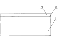
图1是本实用新型的结构示意图。Fig. 1 is the structural representation of the utility model.
图中:1.硅片,2.二氧化硅薄膜,3.氮化硅薄膜。In the figure: 1. Silicon wafer, 2. Silicon dioxide film, 3. Silicon nitride film.
具体实施方式Detailed ways
现在结合附图对本实用新型作进一步详细的说明。这些附图均为简化的示意图,仅以示意方式说明本实用新型的基本结构,因此其仅显示与本实用新型有关的构成。Now in conjunction with accompanying drawing, the utility model is described in further detail. These drawings are all simplified schematic diagrams, and only schematically illustrate the basic structure of the utility model, so they only show the configurations related to the utility model.
如图1所示的晶体硅太阳能电池钝化膜,具有硅片1,在硅片1的上表面具有一层在热硝酸液体中生长形成的超薄的起钝化作用的二氧化硅薄膜2,二氧化硅薄膜2的上表面具有一层氮化硅薄膜3。The passivation film of crystalline silicon solar cell as shown in Figure 1 has a silicon chip 1, and on the upper surface of the silicon chip 1, there is an ultra-thin
对硅片1进行去磷硅玻璃后,硅片1进行刻边,将硅片1放入氟化氢液体去磷硅玻璃,在热氧化液体中浸泡硅片生长二氧化硅薄膜2,再在二氧化硅薄膜2上镀一层氮化硅薄膜3,形成晶体硅太阳能电池的钝化膜。After the silicon wafer 1 is dephosphorous silicon glass, the silicon wafer 1 is edged, the silicon wafer 1 is put into the hydrogen fluoride liquid dephosphoric silicon glass, the silicon wafer is soaked in the thermal oxidation liquid to grow the
本实用新型通过目前发展的低温液体氧化工艺的实现及与目前液体E-etched工艺的整合,来实现在硅片扩散后及氮化硅镀膜间的边刻,去磷硅玻璃及超薄二氧化硅超薄膜制备,作为达到低成本提高太阳能电池性能作用的方法。The utility model implements the low-temperature liquid oxidation process developed at present and integrates with the current liquid E-etched process to realize edge engraving between silicon wafer diffusion and silicon nitride coating, dephosphorous silicon glass and ultra-thin dioxide Silicon ultra-thin film preparation, as a method to improve the performance of solar cells at low cost.
在正常晶硅电池工艺的基础上,在硅片结扩散与ARC减反膜制备之间,在原有的刻边及去磷硅玻璃的基础上实现液体二氧化硅超薄膜上表面钝化加强膜制备,其中采用的热氧化液体,其中热浓硝酸已被证明有效,其他参考液体有双氧水、次氯酸、浓硫酸等。On the basis of the normal crystalline silicon cell technology, between the junction diffusion of the silicon wafer and the preparation of the ARC anti-reflection film, the passivation enhancement film on the upper surface of the liquid silicon dioxide ultra-thin film is realized on the basis of the original edge cutting and phosphorus-removed silicon glass Preparation, the thermal oxidation liquid used in it, in which hot concentrated nitric acid has been proven effective, other reference liquids include hydrogen peroxide, hypochlorous acid, concentrated sulfuric acid, etc.
本实用新型的制作方法:The preparation method of the present utility model:
实施例1:Example 1:
将硅片放入具有一体化液体环境的设备中,对硅片进行清洗、扩散,在硝酸或氟化氢对硅片的背面进行去磷硅玻璃及刻边,再用氟化氢浸泡,将硅片放入热氧化液体中浸泡生长超薄的二氧化硅薄膜,在二氧化硅薄膜上镀一层氮化硅,形成氮化硅薄膜。Put the silicon wafer into the equipment with an integrated liquid environment, clean and diffuse the silicon wafer, dephosphorize silicon glass and cut edges on the back of the silicon wafer in nitric acid or hydrogen fluoride, then soak in hydrogen fluoride, put the silicon wafer into An ultra-thin silicon dioxide film is grown by immersing in a thermal oxidation liquid, and a layer of silicon nitride is coated on the silicon dioxide film to form a silicon nitride film.
实施例2:Example 2:
将硅片进行等离子干刻和液体湿刻,对硅片进行清洗、扩散,再对硅片进行等离子刻边,用氟化氢浸泡硅片并去磷硅玻璃,将硅片放入热氧化液体中浸泡生长超薄的二氧化硅薄膜,在二氧化硅薄膜上镀一层氮化硅,形成氮化硅薄膜。Perform plasma dry etching and liquid wet etching on the silicon wafer, clean and diffuse the silicon wafer, and then perform plasma edge cutting on the silicon wafer, soak the silicon wafer with hydrogen fluoride and remove phosphorus silicon glass, put the silicon wafer into the thermal oxidation liquid and soak An ultra-thin silicon dioxide film is grown, and a layer of silicon nitride is plated on the silicon dioxide film to form a silicon nitride film.
实施例3:Example 3:
将硅片放入具有一体化液体环境的设备中或进行等离子干刻和液体湿刻,对硅片进行、扩散,在氟化氢浸泡硅片,将硅片放入热氧化液体中浸泡生长超薄的二氧化硅薄膜,在二氧化硅薄膜上镀一层氮化硅,形成氮化硅薄膜。Put the silicon wafer into the equipment with an integrated liquid environment or perform plasma dry etching and liquid wet etching, process, diffuse the silicon wafer, soak the silicon wafer in hydrogen fluoride, put the silicon wafer into the thermal oxidation liquid to grow ultra-thin A silicon dioxide film is coated with a layer of silicon nitride on the silicon dioxide film to form a silicon nitride film.
二氧化硅薄膜和氮化硅薄膜钝化的最终效果需通过烧结等热处理工序的体现出来。The final effect of silicon dioxide film and silicon nitride film passivation needs to be reflected through heat treatment processes such as sintering.
Claims (1)
Priority Applications (1)
| Application Number | Priority Date | Filing Date | Title |
|---|---|---|---|
| CN2010201665118U CN201655813U (en) | 2010-04-20 | 2010-04-20 | Passive film for crystalline silicon solar battery |
Applications Claiming Priority (1)
| Application Number | Priority Date | Filing Date | Title |
|---|---|---|---|
| CN2010201665118U CN201655813U (en) | 2010-04-20 | 2010-04-20 | Passive film for crystalline silicon solar battery |
Publications (1)
| Publication Number | Publication Date |
|---|---|
| CN201655813U true CN201655813U (en) | 2010-11-24 |
Family
ID=43121057
Family Applications (1)
| Application Number | Title | Priority Date | Filing Date |
|---|---|---|---|
| CN2010201665118U Expired - Fee Related CN201655813U (en) | 2010-04-20 | 2010-04-20 | Passive film for crystalline silicon solar battery |
Country Status (1)
| Country | Link |
|---|---|
| CN (1) | CN201655813U (en) |
Cited By (9)
| Publication number | Priority date | Publication date | Assignee | Title |
|---|---|---|---|---|
| CN102110742A (en) * | 2010-11-30 | 2011-06-29 | 奥特斯维能源(太仓)有限公司 | Method for passivating crystal silicon P-type surface |
| CN102169924A (en) * | 2011-03-11 | 2011-08-31 | 浙江贝盛光伏股份有限公司 | Crystalline silica solar battery and method for passivating the same |
| CN102290490A (en) * | 2011-08-31 | 2011-12-21 | 无锡赛晶太阳能有限公司 | Preparation technology for dual-film passivated solar cell |
| CN102364698A (en) * | 2011-06-30 | 2012-02-29 | 常州天合光能有限公司 | Solar cell preparation method for secondary utilization of diffusion oxide layer |
| CN102751339A (en) * | 2012-05-08 | 2012-10-24 | 常州天合光能有限公司 | Heterojunction solar cell structure and manufacturing method thereof |
| CN103928535A (en) * | 2014-04-25 | 2014-07-16 | 中利腾晖光伏科技有限公司 | Anti-PID crystalline silicon battery and preparation method thereof |
| CN104014303A (en) * | 2014-05-09 | 2014-09-03 | 奉向东 | Composite material applied to suspension pollution treatment and preparation method of composite material |
| CN104143590A (en) * | 2014-08-08 | 2014-11-12 | 中国科学院宁波材料技术与工程研究所 | Simple and fast silicon surface passivation method |
| CN110416323A (en) * | 2019-07-10 | 2019-11-05 | 天津爱旭太阳能科技有限公司 | A kind of back metal contact zone has the PERC battery and preparation method thereof of passivation layer |
-
2010
- 2010-04-20 CN CN2010201665118U patent/CN201655813U/en not_active Expired - Fee Related
Cited By (10)
| Publication number | Priority date | Publication date | Assignee | Title |
|---|---|---|---|---|
| CN102110742A (en) * | 2010-11-30 | 2011-06-29 | 奥特斯维能源(太仓)有限公司 | Method for passivating crystal silicon P-type surface |
| CN102169924A (en) * | 2011-03-11 | 2011-08-31 | 浙江贝盛光伏股份有限公司 | Crystalline silica solar battery and method for passivating the same |
| CN102364698A (en) * | 2011-06-30 | 2012-02-29 | 常州天合光能有限公司 | Solar cell preparation method for secondary utilization of diffusion oxide layer |
| CN102290490A (en) * | 2011-08-31 | 2011-12-21 | 无锡赛晶太阳能有限公司 | Preparation technology for dual-film passivated solar cell |
| CN102751339A (en) * | 2012-05-08 | 2012-10-24 | 常州天合光能有限公司 | Heterojunction solar cell structure and manufacturing method thereof |
| CN103928535A (en) * | 2014-04-25 | 2014-07-16 | 中利腾晖光伏科技有限公司 | Anti-PID crystalline silicon battery and preparation method thereof |
| CN104014303A (en) * | 2014-05-09 | 2014-09-03 | 奉向东 | Composite material applied to suspension pollution treatment and preparation method of composite material |
| CN104143590A (en) * | 2014-08-08 | 2014-11-12 | 中国科学院宁波材料技术与工程研究所 | Simple and fast silicon surface passivation method |
| CN104143590B (en) * | 2014-08-08 | 2017-08-25 | 中国科学院宁波材料技术与工程研究所 | A kind of simple and quick silicon face passivating method |
| CN110416323A (en) * | 2019-07-10 | 2019-11-05 | 天津爱旭太阳能科技有限公司 | A kind of back metal contact zone has the PERC battery and preparation method thereof of passivation layer |
Similar Documents
| Publication | Publication Date | Title |
|---|---|---|
| CN201655813U (en) | Passive film for crystalline silicon solar battery | |
| CN105226112B (en) | A kind of preparation method of high-efficiency crystalline silicon solar cell | |
| CN102185035B (en) | Process for preparing crystalline silicon solar cell by secondary texturing method | |
| CN101976701B (en) | Manufacturing method of back passivated cell | |
| CN104993019A (en) | Preparation method of localized back contact solar cell | |
| CN102768951A (en) | Method for preparing black silicon by metallic copper ion auxiliary etching | |
| CN103337560A (en) | Preparation method of three-dimensional silicon nano structure for solar cell | |
| CN105513956A (en) | Solar cell corrosion cutting method and solar cell produced by same | |
| CN104701392A (en) | Preparation method of solar battery with low-reflectivity black silicon | |
| CN102339902A (en) | Method and structure of p-type solar cell prepared by mask diffusion method | |
| CN102157585B (en) | Method for manufacturing uniform shallow emitter solar cell | |
| CN102244136A (en) | Method for preparing interdigital back contact double-sided solar cell | |
| CN102623559A (en) | Process for preparing emitter without dead layer of solar cell by oxidation | |
| CN103165760B (en) | A kind of selective doping method of solar cell | |
| CN101673782B (en) | Preparation method of metallurgy-prepared polysilicon solar cell | |
| CN102237433A (en) | Method for oxidizing and passivating liquid of crystalline silicon solar cell | |
| CN102881754B (en) | Back point contact cell with bubbling-free aluminum oxide and preparation method thereof | |
| CN102709386A (en) | Method for preparing full back electrode solar battery | |
| CN104134706A (en) | Graphene silicon solar cell and manufacturing method thereof | |
| CN102255000B (en) | Preparing method of solar cell slice with pattern | |
| CN109216474B (en) | Double oxide layer PERC cell and preparation method thereof | |
| CN101958364A (en) | A kind of production method of backside passivated solar cell | |
| CN202004005U (en) | RIE texturing crystal silicon cell with passivation front side | |
| CN102489468B (en) | Method for cleaning silicon nitride on surface layer of graphite base plate | |
| CN204741023U (en) | Novel flexible solar panel |
Legal Events
| Date | Code | Title | Description |
|---|---|---|---|
| C14 | Grant of patent or utility model | ||
| GR01 | Patent grant | ||
| C17 | Cessation of patent right | ||
| CF01 | Termination of patent right due to non-payment of annual fee |
Granted publication date: 20101124 Termination date: 20130420 |