EP0021404B1 - Datenverarbeitungssystem zur Simulation logischer Operationen - Google Patents
Datenverarbeitungssystem zur Simulation logischer Operationen Download PDFInfo
- Publication number
- EP0021404B1 EP0021404B1 EP80103561A EP80103561A EP0021404B1 EP 0021404 B1 EP0021404 B1 EP 0021404B1 EP 80103561 A EP80103561 A EP 80103561A EP 80103561 A EP80103561 A EP 80103561A EP 0021404 B1 EP0021404 B1 EP 0021404B1
- Authority
- EP
- European Patent Office
- Prior art keywords
- logic
- processor
- instruction
- memory
- data
- Prior art date
- Legal status (The legal status is an assumption and is not a legal conclusion. Google has not performed a legal analysis and makes no representation as to the accuracy of the status listed.)
- Expired
Links
Images


Classifications
-
- G—PHYSICS
- G06—COMPUTING OR CALCULATING; COUNTING
- G06F—ELECTRIC DIGITAL DATA PROCESSING
- G06F30/00—Computer-aided design [CAD]
- G06F30/30—Circuit design
- G06F30/32—Circuit design at the digital level
- G06F30/33—Design verification, e.g. functional simulation or model checking
Definitions
- the advantages offered by the invention are that due to the parallel arrangement of the simulating computing system, the cost of the simulation is decreased and the speed and capacity are increased.
- the logic simulation machine Since the logic simulation machine is not a general purpose computer, it must be used as a device attached to a computer, which can perform functions such as compilation, input/output control, etc.
- the system in which the logic simulation machine will initially be used actually contains two general purpose computers in addition to the logic simulation machine.
- inter-processor switch 33 in a logic simulation machine 50. It provides communication among the thirty-one basic processors and between them and the control processor 32. Its primary purpose is to communicate simulated logic signals from the basic processor generating them to basic processors using them. In addition, it provides communication between the basic processors 1-31 and the control processor 32 for loading the basic processors, transferring inputs and outputs to the local computer, etc.
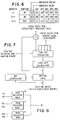
- the logic functions specified in the logic simulation machine instructions are defined by the contents of another basic processor memory, the function memory 37 shown in Fig. 1.
- the relation of the function memory 37 to other basic processor elements is illustrated in Fig. 1.
- the first instruction in the table selects an immediate logical 0 as its sixth input.
- the other two use the previous instruction's output as the sixth input, so their immediate fields are irrelevant (indicated by Xs in the table).
- the functions shown (two ORs followed by a NOR) cause the last instruction's output to be the NOR of all 15 inputs.
- the output of the logic unit which is the value stored in next signal value memory, is a function (AND or OR) of the current dot accumulator contents and the output of the current instruction (logic unit accumulator contents). This final value may be saved in the dot accumulator by using the SAVE FOR DOT flag.
- the logic unit accumulator contents for the current instruction is stored directly into the next signal value memory. No interaction with the current contents of the dot accumulator occurs.
- each basic processor has two additional internal logic data memories. These are identical to the current and next signal value memories 35 and 36 previously discussed. Like the signal value memories 35 and 36, these additional memories alternately assume one of two roles: that of the current signal input memory 38 and that of the next signal input memory 39. Their functions will be described in terms of these roles.
- the actual data memories have been called the A-IN memory and the B-IN memory.
- the current and next signal input memories 38 and 39 contain representations of logic signals. Both have 1024 locations, each holding one signal.
- the data in current signal input memory 38 are logic signal values that are currently present in the simulation, and were generated by other basic processors. This data is selected by use of ADDRESS SOURCE flags in each basic processor instruction. Each of the five addresses in an instruction has an associated ADDRESS SOURCE flag. When it is 0, the address references data in current signal value memory; when 1, the address references data in current signal input memory. Thus any or all of the data used in computing logic function can come from other processors.
- next signal input memory 39 In the course of a major cycle, updated values are obtained from the inter-processor switch 33 and placed in the next signal input memory 39; and at the end of each major cycle, the former next signal input memory is designated to be the current signal input memory (and visa versa).
- the switch select memory 40 of each basic processor has 1024 locations, each containing the address of a basic processor.
- the inter-processor switch 33 uses the switch select memory 40 to place updated logic signal values in the next signal input memory 39 as follows:
- the table of Fig. 11 shows a 2 in processor 3's 49th switch select memory location. This places the needed value in processor 3's 49th next signal input memory 39, so the table of Fig. 12 shows processor 3's 18th instruction accessing that location with its second address.
- the other table elements are derived similarly. It should be noted that at minor cycle 18, Processor 1 simultaneously transmits and receives, sending data to Processors 2 and 3 and obtaining it from Processor 3.
- the scheduling problem must be solved by the logic simulation machine compiler for each device to be simulated. Just as physical components must be placed and wired, simulated logic must be partitioned among the processors and scheduled.
- the control processor 32 of the logic simulation machine provides two functions of particular interest, they are organizing signal values into functional groups so that they can read from or write into the logic simulation machine with a single local computer (51) input/output operation, and halting the logic simulation machine and interrupting the local computer when any of a group of selected signals are set to specified values.
- the first function provides for efficient application of input sequences and gathering of data by the local computer.
- the halting function is the basic mechanism for informing the local computer of events in the simulation such as user-defined events or requests for array read or write.
- the control processor including these two functions are discussed as follows.
- the control processor also provides general logic simulation machine control function, such as, starting the logic simulation machine, halting it, etc. These are provided via commands from the local computer which utilize the control processor in a transparent manner.
- the control processor contains six memories referred to as a switch select memory, an output signal memory, an input signal memory, an output permutation memory, an input permutation memory, and an event mask.
- the input and output signal memories serve as a sink and a source, respectively, of logic data communicated between the control processor 32 and the basic processors 1-31 via the inter- processor switch 33. Both has 1024 locations, each holding a single signal.
- the function of the input and output permutation memories is to permute the transmission order of values in the input and output signal memories respectively.
- Each of these memories contains 1024 locations of 10 bits each; an address in the associated signal memory is contained in each location.
- This permutation of signal order allows data to be functionally grouped in the output signal memory, minimizing the local computer input/output operations needed to alter it. Such functional grouping might otherwise be impossible to achieve, due to the requirements of scheduling inter- processor data transfers through the inter-processor switch 33.
- a set of test inputs can be positioned in contiguous locations of the output signal memory and stored there with a single local computer input/output operation; appropriate output permutation memory contents can then feed that data to the switch at the minor cycles to which they have been scheduled for conflict-free inter- processor communication.
- the event mask contains 1024 locations of 4 bits each. Each of the bits corresponds to an individual value of the 2-bit code for simulated signal values: the first bit corresponds to 00, the second to 01, the third to 10, and the last to 11.
- the event mask in parallel with the output and input permutation memories of control processor 32, is cycled through in address order as part of a major cycle. As each signal value is received from the inter-processor switch 33, it is matched against the contents of the current event mask location. If the location contains a "1" corresponding to the signal value, the simulator is halted at the end of the current major cycle and an interrupt is presented to the local computer.
- event mask locations correspond to signal values in the order they are received from the switch, not in the (permuted) order of storage in input signal memory.
- any of several values of a particular signal can be made to cause the simulator to halt.
- the simulator could be halted when a particular signal is set to anything except logical 0.
- the control processor also contains two identical counters called level counter 1 and level counter 2, each 16 bits long. They can be loaded via local computer input/output commands, and are decremented each major cycle. When either reaches 0, the local computer is interrupted.
- These counters can be used for various purposes. For example, one can count the major cycles (gate delays) per logic cycle of the simulated device, giving the local computer an interrupt when it is time to gather an output vector and apply a new input vector. The other can count the total number of major cycles a simulation is to run.
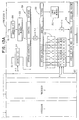
- control processor 32 also shown in Fig. 1, which is shown on Fig. 13C and 13D. Control processor 32 will be described in detail later and as previously stated is used mainly to accumulate the result and to provide the control pulses which are needed for the entire logic simulation machine of this embodiment.
- the B and B IN memories will be read.
- the switching between the A and A IN and the B and B IN memories is accomplished by the switching mechanism indicated by the dotted line 212 on Fig. 13A. If it be assumed that, in a certain major cycle, the A and A IN memories are read out of in this same major cycle, the B and B IN memories can be read into. When the A and A IN memories are read out of, these two memories are regarded as a single memory.
- the A and the A IN are both memories addressed by the low order ten bits of the operand in register 206 while the high order bit of this same operand selects which of the two (A or A IN) memories is actually read. In other words, the operands in register 206 are eleven bits.
- each one of these memories are regarded as separate memories and are both addressed by ten bits which is contained in the address register 214 on Fig. 13A. These memories will be described in much more detail later on in the description.
- the pulse produced by the AND circuit 270 at this time extends the flip flop device 256 to reset it to its "0" state thus turning off the pulse generator 258.
- the same pulse is also applied to gate 262 in order to test "event latch” 260. If the latch 260 is still on its “0” state, a pulse will be produced on wire 272, which extends through OR circuit 248 to again turn “on” single shot device 250 in order to start a new major cycle. If the "event latch” 260 is in its "1” state, a pulse will appear on lead 274 to signal the end of operations.
- This timing chart of Fig. 13E will be understood better when the detailed circuits shown in the remaining figures are described.
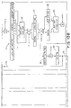
- Figs. 16A and 16B arranged as shown in Fig. 16 which is a detail of the inter-processor switch which is indicated in Fig. 1 and by the dotted lines on the left side of Figs. 13A and 13D.
- the inter-processor switch has its own address counter 290 which supplies addresses to the switch memory 292.
- Memory words are placed into the register 294 by the P-1 gate pulse and later transferred to register 296 by the P-2 gate pulse.
- the groups of leads from each one of these decoders is applied to gates such as 298, 300, 302 and 304.
- FIG. 17A shows how the information in the register 216, which is also shown on Fig. 13B, refers to the logic unit for step one and how the control bits are directed to gates which suitably control the logic.
- the results of the logic unit first step are passed along with certain of the control bits in register 216 (Fig. 13B) to the logic unit second step shown in Fig. 17B.
- the Boolean logic equations for the logic unit second step are shown in Fig. 17B and it is believed that there will be no difficulty in understanding the operation of this unit.
- the "logic unit first step” shown in Fig. 17A carries out specific logic functions.
- the inputs to “logic unit first step” accepts and as shown in Fig. 17A.
- conventional logic circuits such as AND gates, OR gates and inverters arranged in a manner well known to those skilled in the art, the following logic operations are performed by the logic unit first step.
- FIG. 18 shows the details of event logic of Fig. 13C.
- the event logic is shown on Fig. 13C with one of its inputs coming from the mask field in register 240 and its input from the cable 244 which comes from the inter-processor switch.
- the data from the mask field in register 240 combines with the data from the inter-processor switch to produce an output of the OR circuit 322 which provides an output on line 324 in order to set the "event latch" 260 to its "1" state. Then, it is said that an "event” has occurred.
- the detection of an "event” causes a signal to appear on lead wire 274 on Fig. 13D which signals the end of operations.
Landscapes
- Engineering & Computer Science (AREA)
- Computer Hardware Design (AREA)
- Physics & Mathematics (AREA)
- Theoretical Computer Science (AREA)
- Evolutionary Computation (AREA)
- Geometry (AREA)
- General Engineering & Computer Science (AREA)
- General Physics & Mathematics (AREA)
- Test And Diagnosis Of Digital Computers (AREA)
- Tests Of Electronic Circuits (AREA)
Claims (6)
Applications Claiming Priority (2)
| Application Number | Priority Date | Filing Date | Title |
|---|---|---|---|
| US53444 | 1979-06-29 | ||
| US06/053,444 US4306286A (en) | 1979-06-29 | 1979-06-29 | Logic simulation machine |
Publications (2)
| Publication Number | Publication Date |
|---|---|
| EP0021404A1 EP0021404A1 (de) | 1981-01-07 |
| EP0021404B1 true EP0021404B1 (de) | 1983-05-11 |
Family
ID=21984277
Family Applications (1)
| Application Number | Title | Priority Date | Filing Date |
|---|---|---|---|
| EP80103561A Expired EP0021404B1 (de) | 1979-06-29 | 1980-06-24 | Datenverarbeitungssystem zur Simulation logischer Operationen |
Country Status (5)
| Country | Link |
|---|---|
| US (1) | US4306286A (de) |
| EP (1) | EP0021404B1 (de) |
| JP (1) | JPS5948424B2 (de) |
| DE (1) | DE3063100D1 (de) |
| IT (1) | IT1150956B (de) |
Families Citing this family (154)
| Publication number | Priority date | Publication date | Assignee | Title |
|---|---|---|---|---|
| JPS57212508A (en) * | 1981-06-25 | 1982-12-27 | Mitsubishi Electric Corp | Programming device with cathode ray tube |
| JPS5814257A (ja) * | 1981-07-17 | 1983-01-27 | Fujitsu Ltd | 論理シミユレ−シヨン用デ−タ処理装置 |
| JPS58146947A (ja) * | 1982-02-26 | 1983-09-01 | Nec Corp | 論理シミユレ−タ |
| DE3221819A1 (de) * | 1982-06-09 | 1984-02-23 | Siemens AG, 1000 Berlin und 8000 München | Vorrichtung zur simulation eines schaltwerks mit hilfe eines rechners |
| US4656580A (en) * | 1982-06-11 | 1987-04-07 | International Business Machines Corporation | Logic simulation machine |
| EP0099114B1 (de) * | 1982-07-13 | 1988-05-11 | Nec Corporation | Logischer Simulator durchführbar auf Ebenenbasis und auf logischer Blockbasis auf jeder Ebene |
| JPS5975347A (ja) * | 1982-10-21 | 1984-04-28 | Toshiba Corp | 論理回路のシミユレ−シヨン装置 |
| US4527249A (en) * | 1982-10-22 | 1985-07-02 | Control Data Corporation | Simulator system for logic design validation |
| US4587625A (en) * | 1983-07-05 | 1986-05-06 | Motorola Inc. | Processor for simulating digital structures |
| WO1985002033A1 (en) * | 1983-11-03 | 1985-05-09 | Prime Computer, Inc. | Digital system simulation method and apparatus |
| US4628471A (en) * | 1984-02-02 | 1986-12-09 | Prime Computer, Inc. | Digital system simulation method and apparatus having two signal-level modes of operation |
| US4751637A (en) * | 1984-03-28 | 1988-06-14 | Daisy Systems Corporation | Digital computer for implementing event driven simulation algorithm |
| US4814983A (en) * | 1984-03-28 | 1989-03-21 | Daisy Systems Corporation | Digital computer for implementing event driven simulation algorithm |
| US4777618A (en) * | 1984-07-19 | 1988-10-11 | Nippondenso Co., Ltd. | Method of storing, indicating or producing signals and apparatus for recording or producing signals |
| JPS6142040A (ja) * | 1984-08-03 | 1986-02-28 | Nec Corp | 論理シミユレ−タ |
| JPS6165336A (ja) * | 1984-09-07 | 1986-04-03 | Hitachi Ltd | 高速演算方式 |
| JPS61102569A (ja) * | 1984-10-26 | 1986-05-21 | Hitachi Ltd | 高速論理シミユレ−シヨン装置 |
| US4819150A (en) | 1985-04-05 | 1989-04-04 | Unisys Corporation | Array for simulating computer functions for large computer systems |
| JPH0743733B2 (ja) * | 1985-12-11 | 1995-05-15 | 株式会社日立製作所 | 論理シミュレーション方法 |
| US5036453A (en) * | 1985-12-12 | 1991-07-30 | Texas Instruments Incorporated | Master/slave sequencing processor |
| US4763289A (en) * | 1985-12-31 | 1988-08-09 | International Business Machines Corporation | Method for the modeling and fault simulation of complementary metal oxide semiconductor circuits |
| US4937770A (en) * | 1986-02-07 | 1990-06-26 | Teradyne, Inc. | Simulation system |
| US4744084A (en) * | 1986-02-27 | 1988-05-10 | Mentor Graphics Corporation | Hardware modeling system and method for simulating portions of electrical circuits |
| US4792909A (en) * | 1986-04-07 | 1988-12-20 | Xerox Corporation | Boolean logic layout generator |
| US4862347A (en) * | 1986-04-22 | 1989-08-29 | International Business Machine Corporation | System for simulating memory arrays in a logic simulation machine |
| JPS62251843A (ja) * | 1986-04-25 | 1987-11-02 | Hitachi Ltd | 論理シミユレ−シヨン方法および装置 |
| US5126966A (en) * | 1986-06-25 | 1992-06-30 | Ikos Systems, Inc. | High speed logic simulation system with stimulus engine using independent event channels selectively driven by independent stimulus programs |
| US4787061A (en) * | 1986-06-25 | 1988-11-22 | Ikos Systems, Inc. | Dual delay mode pipelined logic simulator |
| US4787062A (en) * | 1986-06-26 | 1988-11-22 | Ikos Systems, Inc. | Glitch detection by forcing the output of a simulated logic device to an undefined state |
| US4821173A (en) * | 1986-06-30 | 1989-04-11 | Motorola, Inc. | Wired "OR" bus evaluator for logic simulation |
| US4815016A (en) * | 1986-07-24 | 1989-03-21 | Unisys Corp. | High speed logical circuit simulator |
| US4827427A (en) * | 1987-03-05 | 1989-05-02 | Hyduke Stanley M | Instantaneous incremental compiler for producing logic circuit designs |
| US5257201A (en) * | 1987-03-20 | 1993-10-26 | International Business Machines Corporation | Method to efficiently reduce the number of connections in a circuit |
| US4816999A (en) * | 1987-05-20 | 1989-03-28 | International Business Machines Corporation | Method of detecting constants and removing redundant connections in a logic network |
| US4872125A (en) * | 1987-06-26 | 1989-10-03 | Daisy Systems Corporation | Multiple processor accelerator for logic simulation |
| US4916647A (en) * | 1987-06-26 | 1990-04-10 | Daisy Systems Corporation | Hardwired pipeline processor for logic simulation |
| US4873656A (en) * | 1987-06-26 | 1989-10-10 | Daisy Systems Corporation | Multiple processor accelerator for logic simulation |
| US4914612A (en) * | 1988-03-31 | 1990-04-03 | International Business Machines Corporation | Massively distributed simulation engine |
| US4989131A (en) * | 1988-07-26 | 1991-01-29 | International Business Machines Corporation | Technique for parallel synchronization |
| US5452231A (en) * | 1988-10-05 | 1995-09-19 | Quickturn Design Systems, Inc. | Hierarchically connected reconfigurable logic assembly |
| US5109353A (en) | 1988-12-02 | 1992-04-28 | Quickturn Systems, Incorporated | Apparatus for emulation of electronic hardware system |
| US5329470A (en) * | 1988-12-02 | 1994-07-12 | Quickturn Systems, Inc. | Reconfigurable hardware emulation system |
| US5572708A (en) * | 1989-02-28 | 1996-11-05 | Nec Corporation | Hardware simulator capable of dealing with a description of a functional level |
| US5353243A (en) * | 1989-05-31 | 1994-10-04 | Synopsys Inc. | Hardware modeling system and method of use |
| US5369593A (en) * | 1989-05-31 | 1994-11-29 | Synopsys Inc. | System for and method of connecting a hardware modeling element to a hardware modeling system |
| US5091872A (en) * | 1989-06-23 | 1992-02-25 | At&T Bell Laboratories | Apparatus and method for performing spike analysis in a logic simulator |
| KR0158887B1 (ko) * | 1990-01-12 | 1999-02-18 | 이노우에 키요시 | 논리 모의실험기 |
| US5375074A (en) * | 1990-01-23 | 1994-12-20 | At&T Corp. | Unboundedly parallel simulations |
| US5161156A (en) * | 1990-02-02 | 1992-11-03 | International Business Machines Corporation | Multiprocessing packet switching connection system having provision for error correction and recovery |
| EP0445454B1 (de) * | 1990-03-08 | 1997-06-18 | International Business Machines Corporation | Hardware-Simulator |
| JPH05205005A (ja) * | 1990-03-30 | 1993-08-13 | Internatl Business Mach Corp <Ibm> | ロジック・シミュレーション・マシン用ホスト・インタフェース |
| US5327361A (en) * | 1990-03-30 | 1994-07-05 | International Business Machines Corporation | Events trace gatherer for a logic simulation machine |
| JPH04116779A (ja) * | 1990-09-07 | 1992-04-17 | Takayama:Kk | データ処理装置 |
| US5291612A (en) * | 1991-02-11 | 1994-03-01 | University Technologies International | System for evaluating boolean expressions using total differential generating tree structured processing elements controlled by partial subfunction differentials |
| US5257266A (en) * | 1991-02-27 | 1993-10-26 | General Dynamics Corporation, Space Systems Division | Computer and communications systems employing universal direct spherics processing architectures |
| US5442772A (en) * | 1991-03-29 | 1995-08-15 | International Business Machines Corporation | Common breakpoint in virtual time logic simulation for parallel processors |
| EP0508619A2 (de) * | 1991-04-11 | 1992-10-14 | Hewlett-Packard Company | Stimulus-Schnittstelle mit bidirektionalem Sockel für einen Logiksimulator |
| GB9121540D0 (en) * | 1991-10-10 | 1991-11-27 | Smiths Industries Plc | Computing systems and methods |
| US5475830A (en) * | 1992-01-31 | 1995-12-12 | Quickturn Design Systems, Inc. | Structure and method for providing a reconfigurable emulation circuit without hold time violations |
| US5425036A (en) * | 1992-09-18 | 1995-06-13 | Quickturn Design Systems, Inc. | Method and apparatus for debugging reconfigurable emulation systems |
| US5452239A (en) * | 1993-01-29 | 1995-09-19 | Quickturn Design Systems, Inc. | Method of removing gated clocks from the clock nets of a netlist for timing sensitive implementation of the netlist in a hardware emulation system |
| US5594741A (en) * | 1993-03-31 | 1997-01-14 | Digital Equipment Corporation | Method for control of random test vector generation |
| IL109921A (en) * | 1993-06-24 | 1997-09-30 | Quickturn Design Systems | Method and apparatus for configuring memory circuits |
| JP3083220B2 (ja) * | 1993-08-09 | 2000-09-04 | 株式会社日立製作所 | 設計支援システム |
| US5680583A (en) * | 1994-02-16 | 1997-10-21 | Arkos Design, Inc. | Method and apparatus for a trace buffer in an emulation system |
| US5815403A (en) * | 1994-04-19 | 1998-09-29 | Lsi Logic Corporation | Fail-safe distributive processing method for producing a highest fitness cell placement for an integrated circuit chip |
| US5963975A (en) * | 1994-04-19 | 1999-10-05 | Lsi Logic Corporation | Single chip integrated circuit distributed shared memory (DSM) and communications nodes |
| US5875117A (en) * | 1994-04-19 | 1999-02-23 | Lsi Logic Corporation | Simultaneous placement and routing (SPAR) method for integrated circuit physical design automation system |
| US6493658B1 (en) | 1994-04-19 | 2002-12-10 | Lsi Logic Corporation | Optimization processing for integrated circuit physical design automation system using optimally switched fitness improvement algorithms |
| US5495419A (en) * | 1994-04-19 | 1996-02-27 | Lsi Logic Corporation | Integrated circuit physical design automation system utilizing optimization process decomposition and parallel processing |
| US6155725A (en) * | 1994-04-19 | 2000-12-05 | Lsi Logic Corporation | Cell placement representation and transposition for integrated circuit physical design automation system |
| US5914887A (en) * | 1994-04-19 | 1999-06-22 | Lsi Logic Corporation | Congestion based cost factor computing apparatus for integrated circuit physical design automation system |
| US5557533A (en) * | 1994-04-19 | 1996-09-17 | Lsi Logic Corporation | Cell placement alteration apparatus for integrated circuit chip physical design automation system |
| US5559718A (en) * | 1994-04-28 | 1996-09-24 | Cadence Design Systems, Inc. | System and method for model-based verification of local design rules |
| US5920712A (en) * | 1994-05-13 | 1999-07-06 | Quickturn Design Systems, Inc. | Emulation system having multiple emulator clock cycles per emulated clock cycle |
| US5551013A (en) * | 1994-06-03 | 1996-08-27 | International Business Machines Corporation | Multiprocessor for hardware emulation |
| US6208954B1 (en) * | 1994-09-16 | 2001-03-27 | Wind River Systems, Inc. | Method for scheduling event sequences |
| US5615127A (en) * | 1994-11-30 | 1997-03-25 | International Business Machines Corporation | Parallel execution of a complex task partitioned into a plurality of entities |
| GB2296619B (en) * | 1994-12-20 | 1998-12-16 | Northern Telecom Ltd | Network emulation tool |
| US5649164A (en) * | 1994-12-30 | 1997-07-15 | International Business Machines Corporation | Sets and holds in virtual time logic simulation for parallel processors |
| US5546562A (en) * | 1995-02-28 | 1996-08-13 | Patel; Chandresh | Method and apparatus to emulate VLSI circuits within a logic simulator |
| US5632028A (en) * | 1995-03-03 | 1997-05-20 | Hal Computer Systems, Inc. | Hardware support for fast software emulation of unimplemented instructions |
| JP3242277B2 (ja) * | 1995-03-20 | 2001-12-25 | 富士通株式会社 | シミュレーション装置 |
| US5706476A (en) * | 1995-06-05 | 1998-01-06 | Synopsys, Inc. | Method and apparatus for use of the undefined logic state and mixed multiple-state abstractions in digital logic simulation |
| US5923865A (en) * | 1995-06-28 | 1999-07-13 | Quickturn Design Systems, Inc. | Emulation system having multiple emulated clock cycles per emulator clock cycle and improved signal routing |
| US5819065A (en) * | 1995-06-28 | 1998-10-06 | Quickturn Design Systems, Inc. | System and method for emulating memory |
| US5819063A (en) * | 1995-09-11 | 1998-10-06 | International Business Machines Corporation | Method and data processing system for emulating a program |
| JP3645346B2 (ja) * | 1996-01-22 | 2005-05-11 | 富士通株式会社 | 論理シミュレーション装置 |
| US5868575A (en) * | 1996-05-20 | 1999-02-09 | Kuczewski; Robert M. | Cooperative/interactive learning system for logic instruction |
| US5822564A (en) * | 1996-06-03 | 1998-10-13 | Quickturn Design Systems, Inc. | Checkpointing in an emulation system |
| US6026223A (en) * | 1996-06-28 | 2000-02-15 | Scepanovic; Ranko | Advanced modular cell placement system with overlap remover with minimal noise |
| US5870311A (en) * | 1996-06-28 | 1999-02-09 | Lsi Logic Corporation | Advanced modular cell placement system with fast procedure for finding a levelizing cut point |
| US5831863A (en) * | 1996-06-28 | 1998-11-03 | Lsi Logic Corporation | Advanced modular cell placement system with wire length driven affinity system |
| US5963455A (en) * | 1996-06-28 | 1999-10-05 | Lsi Logic Corporation | Advanced modular cell placement system with functional sieve optimization technique |
| US5812740A (en) * | 1996-06-28 | 1998-09-22 | Lsi Logic Corporation | Advanced modular cell placement system with neighborhood system driven optimization |
| US6067409A (en) * | 1996-06-28 | 2000-05-23 | Lsi Logic Corporation | Advanced modular cell placement system |
| US5914888A (en) * | 1996-06-28 | 1999-06-22 | Lsi Logic Corporation | Advanced modular cell placement system with coarse overflow remover |
| US6085032A (en) * | 1996-06-28 | 2000-07-04 | Lsi Logic Corporation | Advanced modular cell placement system with sinusoidal optimization |
| US5892688A (en) * | 1996-06-28 | 1999-04-06 | Lsi Logic Corporation | Advanced modular cell placement system with iterative one dimensional preplacement optimization |
| US6030110A (en) * | 1996-06-28 | 2000-02-29 | Lsi Logic Corporation | Advanced modular cell placement system with median control and increase in resolution |
| US5870312A (en) * | 1996-06-28 | 1999-02-09 | Lsi Logic Corporation | Advanced modular cell placement system with dispersion-driven levelizing system |
| US5835381A (en) * | 1996-06-28 | 1998-11-10 | Lsi Logic Corporation | Advanced modular cell placement system with minimizing maximal cut driven affinity system |
| US5808899A (en) * | 1996-06-28 | 1998-09-15 | Lsi Logic Corporation | Advanced modular cell placement system with cell placement crystallization |
| US5872718A (en) * | 1996-06-28 | 1999-02-16 | Lsi Logic Corporation | Advanced modular cell placement system |
| US5867398A (en) * | 1996-06-28 | 1999-02-02 | Lsi Logic Corporation | Advanced modular cell placement system with density driven capacity penalty system |
| US5844811A (en) * | 1996-06-28 | 1998-12-01 | Lsi Logic Corporation | Advanced modular cell placement system with universal affinity driven discrete placement optimization |
| US5959993A (en) * | 1996-09-13 | 1999-09-28 | Lsi Logic Corporation | Scheduler design for ATM switches, and its implementation in a distributed shared memory architecture |
| US5831980A (en) * | 1996-09-13 | 1998-11-03 | Lsi Logic Corporation | Shared memory fabric architecture for very high speed ATM switches |
| US5886904A (en) * | 1996-09-23 | 1999-03-23 | Quickturn Design Systems, Inc. | Latch optimization in hardware logic emulation systems |
| US5841967A (en) * | 1996-10-17 | 1998-11-24 | Quickturn Design Systems, Inc. | Method and apparatus for design verification using emulation and simulation |
| US5980093A (en) * | 1996-12-04 | 1999-11-09 | Lsi Logic Corporation | Integrated circuit layout routing using multiprocessing |
| US5920485A (en) * | 1996-12-05 | 1999-07-06 | Hewlett-Packard | Method of selecting gates for efficient code generation by a circuit compiler |
| US6141636A (en) * | 1997-03-31 | 2000-10-31 | Quickturn Design Systems, Inc. | Logic analysis subsystem in a time-sliced emulator |
| US6421251B1 (en) | 1997-05-02 | 2002-07-16 | Axis Systems Inc | Array board interconnect system and method |
| US6009256A (en) * | 1997-05-02 | 1999-12-28 | Axis Systems, Inc. | Simulation/emulation system and method |
| US6389379B1 (en) | 1997-05-02 | 2002-05-14 | Axis Systems, Inc. | Converification system and method |
| US6321366B1 (en) | 1997-05-02 | 2001-11-20 | Axis Systems, Inc. | Timing-insensitive glitch-free logic system and method |
| US6134516A (en) * | 1997-05-02 | 2000-10-17 | Axis Systems, Inc. | Simulation server system and method |
| US6026230A (en) * | 1997-05-02 | 2000-02-15 | Axis Systems, Inc. | Memory simulation system and method |
| US5960191A (en) * | 1997-05-30 | 1999-09-28 | Quickturn Design Systems, Inc. | Emulation system with time-multiplexed interconnect |
| US5970240A (en) * | 1997-06-25 | 1999-10-19 | Quickturn Design Systems, Inc. | Method and apparatus for configurable memory emulation |
| US6266802B1 (en) | 1997-10-27 | 2001-07-24 | International Business Machines Corporation | Detailed grid point layout using a massively parallel logic including an emulator/simulator paradigm |
| US6016563A (en) * | 1997-12-30 | 2000-01-18 | Fleisher; Evgeny G. | Method and apparatus for testing a logic design of a programmable logic device |
| US6279146B1 (en) | 1999-01-06 | 2001-08-21 | Simutech Corporation | Apparatus and method for verifying a multi-component electronic design |
| US6832182B1 (en) | 1999-04-08 | 2004-12-14 | Transim Technology Corporation | Circuit simulator |
| US6618698B1 (en) | 1999-08-12 | 2003-09-09 | Quickturn Design Systems, Inc. | Clustered processors in an emulation engine |
| US6931572B1 (en) | 1999-11-30 | 2005-08-16 | Synplicity, Inc. | Design instrumentation circuitry |
| US7072818B1 (en) | 1999-11-30 | 2006-07-04 | Synplicity, Inc. | Method and system for debugging an electronic system |
| US7065481B2 (en) | 1999-11-30 | 2006-06-20 | Synplicity, Inc. | Method and system for debugging an electronic system using instrumentation circuitry and a logic analyzer |
| US7356786B2 (en) | 1999-11-30 | 2008-04-08 | Synplicity, Inc. | Method and user interface for debugging an electronic system |
| US6823497B2 (en) | 1999-11-30 | 2004-11-23 | Synplicity, Inc. | Method and user interface for debugging an electronic system |
| US6581191B1 (en) | 1999-11-30 | 2003-06-17 | Synplicity, Inc. | Hardware debugging in a hardware description language |
| US6578133B1 (en) * | 2000-02-24 | 2003-06-10 | Stanley M. Hyduke | MIMD array of single bit processors for processing logic equations in strict sequential order |
| US7222315B2 (en) | 2000-11-28 | 2007-05-22 | Synplicity, Inc. | Hardware-based HDL code coverage and design analysis |
| US6898562B2 (en) | 2000-12-07 | 2005-05-24 | International Business Machines Corporation | Method and system for efficiently overriding net values in a logic simulator machine |
| US20030149962A1 (en) * | 2001-11-21 | 2003-08-07 | Willis John Christopher | Simulation of designs using programmable processors and electronically re-configurable logic arrays |
| US7328195B2 (en) * | 2001-11-21 | 2008-02-05 | Ftl Systems, Inc. | Semi-automatic generation of behavior models continuous value using iterative probing of a device or existing component model |
| US7260794B2 (en) * | 2002-12-20 | 2007-08-21 | Quickturn Design Systems, Inc. | Logic multiprocessor for FPGA implementation |
| US7698118B2 (en) | 2004-04-15 | 2010-04-13 | Mentor Graphics Corporation | Logic design modeling and interconnection |
| US7738398B2 (en) * | 2004-06-01 | 2010-06-15 | Quickturn Design Systems, Inc. | System and method for configuring communication systems |
| JP4530883B2 (ja) * | 2004-09-30 | 2010-08-25 | 富士通セミコンダクター株式会社 | シミュレーションモデル生成方法 |
| US7174265B2 (en) * | 2005-05-13 | 2007-02-06 | International Business Machines Corporation | Heterogeneous multipath path network test system |
| US7509602B2 (en) * | 2005-06-02 | 2009-03-24 | Eve S.A. | Compact processor element for a scalable digital logic verification and emulation system |
| US20070043548A1 (en) * | 2005-07-29 | 2007-02-22 | International Business Machines Corporation | Verifying a simulated hardware environment for a simulated device under test |
| US7562001B2 (en) | 2005-07-29 | 2009-07-14 | International Business Machines Corporation | Creating a behavioral model of a hardware device for use in a simulation environment |
| WO2007104930A1 (en) * | 2006-03-10 | 2007-09-20 | Imperas Ltd | Method of developing a multi-processor system |
| US7555424B2 (en) | 2006-03-16 | 2009-06-30 | Quickturn Design Systems, Inc. | Method and apparatus for rewinding emulated memory circuits |
| US7934179B2 (en) * | 2006-11-20 | 2011-04-26 | Et International, Inc. | Systems and methods for logic verification |
| US8234624B2 (en) | 2007-01-25 | 2012-07-31 | International Business Machines Corporation | System and method for developing embedded software in-situ |
| US7945433B2 (en) * | 2007-04-30 | 2011-05-17 | International Business Machines Corporation | Hardware simulation accelerator design and method that exploits a parallel structure of user models to support a larger user model size |
| US20100057427A1 (en) * | 2008-09-04 | 2010-03-04 | Anthony Dean Walker | Simulated processor execution using branch override |
| US8959010B1 (en) | 2011-12-08 | 2015-02-17 | Cadence Design Systems, Inc. | Emulation system with improved reliability of interconnect and a method for programming such interconnect |
| US8743735B1 (en) | 2012-01-18 | 2014-06-03 | Cadence Design Systems, Inc. | Emulation system for verifying a network device |
| US8595683B1 (en) | 2012-04-12 | 2013-11-26 | Cadence Design Systems, Inc. | Generating user clocks for a prototyping environment |
Family Cites Families (28)
| Publication number | Priority date | Publication date | Assignee | Title |
|---|---|---|---|---|
| US3308285A (en) * | 1963-04-19 | 1967-03-07 | Rca Corp | Logic networks for realizing associative logic functions |
| US3278732A (en) * | 1963-10-29 | 1966-10-11 | Ibm | High speed multiplier circuit |
| GB1101851A (en) * | 1965-01-20 | 1968-01-31 | Ncr Co | Generalized logic circuitry |
| US3381117A (en) * | 1965-08-02 | 1968-04-30 | Ibm | Minimal pin multipurpose logic circuits |
| US3458240A (en) * | 1965-12-28 | 1969-07-29 | Sperry Rand Corp | Function generator for producing the possible boolean functions of eta independent variables |
| US3544973A (en) * | 1968-03-13 | 1970-12-01 | Westinghouse Electric Corp | Variable structure computer |
| US3634830A (en) * | 1969-06-13 | 1972-01-11 | Ibm | Modular computer sharing system with intercomputer communication control apparatus |
| US3614745A (en) * | 1969-09-15 | 1971-10-19 | Ibm | Apparatus and method in a multiple operand stream computing system for identifying the specification of multitasks situations and controlling the execution thereof |
| US3702011A (en) * | 1970-05-12 | 1972-10-31 | Bell Telephone Labor Inc | Apparatus and method for simulating logic faults |
| US3701976A (en) * | 1970-07-13 | 1972-10-31 | Bell Telephone Labor Inc | Floating point arithmetic unit for a parallel processing computer |
| DE2106257A1 (de) * | 1971-02-10 | 1972-08-24 | Philips Patentverwaltung | Computer-Lehrspiel |
| US3823321A (en) * | 1971-08-20 | 1974-07-09 | Siemens Ag | Particle-beam apparatus such as an electron microscope or the like |
| US3810114A (en) * | 1971-12-29 | 1974-05-07 | Tokyo Shibaura Electric Co | Data processing system |
| GB1362314A (en) * | 1972-08-08 | 1974-08-07 | Ibm | Method for programming a computer to simulate a digital circuit |
| US4087794A (en) * | 1973-01-02 | 1978-05-02 | International Business Machines Corporation | Multi-level storage hierarchy emulation monitor |
| US3921146A (en) * | 1973-01-05 | 1975-11-18 | Gen Electric | Programmable data processor and controller system |
| US3913070A (en) * | 1973-02-20 | 1975-10-14 | Memorex Corp | Multi-processor data processing system |
| DE2321200C3 (de) * | 1973-04-26 | 1984-01-26 | Siemens AG, 1000 Berlin und 8000 München | Schaltungsanordnung zur Durchführung logischer, durch Boolesche Gleichungen dargestellter Verknüpfungen |
| US3944985A (en) * | 1973-10-19 | 1976-03-16 | Texas Instruments Incorporated | Workspace addressing system |
| FR2258113A5 (de) * | 1973-11-30 | 1975-08-08 | Honeywell Bull Soc Ind | |
| GB1474385A (en) * | 1973-12-14 | 1977-05-25 | Int Computers Ltd | Multiprocessor data processing systems |
| US4050058A (en) * | 1973-12-26 | 1977-09-20 | Xerox Corporation | Microprocessor with parallel operation |
| US4065808A (en) * | 1975-01-25 | 1977-12-27 | U.S. Philips Corporation | Network computer system |
| JPS51117833A (en) * | 1975-04-09 | 1976-10-16 | Hitachi Ltd | Group control system |
| US4015246A (en) * | 1975-04-14 | 1977-03-29 | The Charles Stark Draper Laboratory, Inc. | Synchronous fault tolerant multi-processor system |
| SE7505552L (sv) * | 1975-05-14 | 1976-11-15 | Ellemtel Utvecklings Ab | Sett och anordning att efter varandra avverka databehandlingsinstruktioner i funktionsenheter hos en datamaskin |
| FR2361718A1 (fr) * | 1976-08-11 | 1978-03-10 | Adersa | Processeur parallele associatif a hierarchie de memoire, notamment pour l'acquisition et le traitement rapides des signaux |
| US4079455A (en) * | 1976-12-13 | 1978-03-14 | Rca Corporation | Microprocessor architecture |
-
1979
- 1979-06-29 US US06/053,444 patent/US4306286A/en not_active Expired - Lifetime
-
1980
- 1980-05-28 JP JP55070225A patent/JPS5948424B2/ja not_active Expired
- 1980-06-06 IT IT22605/80A patent/IT1150956B/it active
- 1980-06-24 EP EP80103561A patent/EP0021404B1/de not_active Expired
- 1980-06-24 DE DE8080103561T patent/DE3063100D1/de not_active Expired
Also Published As
| Publication number | Publication date |
|---|---|
| DE3063100D1 (en) | 1983-06-16 |
| JPS567167A (en) | 1981-01-24 |
| IT8022605A0 (it) | 1980-06-06 |
| US4306286A (en) | 1981-12-15 |
| JPS5948424B2 (ja) | 1984-11-26 |
| IT1150956B (it) | 1986-12-17 |
| EP0021404A1 (de) | 1981-01-07 |
Similar Documents
| Publication | Publication Date | Title |
|---|---|---|
| EP0021404B1 (de) | Datenverarbeitungssystem zur Simulation logischer Operationen | |
| EP0096176B1 (de) | Logische Simulationsverfahren und logisches Simulationsgerät | |
| US4527249A (en) | Simulator system for logic design validation | |
| US5418952A (en) | Parallel processor cell computer system | |
| EP0450839A2 (de) | Logiksimulationsmaschine | |
| US5721953A (en) | Interface for logic simulation using parallel bus for concurrent transfers and having FIFO buffers for sending data to receiving units when ready | |
| US4937770A (en) | Simulation system | |
| US6141636A (en) | Logic analysis subsystem in a time-sliced emulator | |
| JPS60218138A (ja) | 事象駆動形アルゴリズムを実行するコンピユータ装置 | |
| US6523155B1 (en) | Method for partitioning a netlist into multiple clock domains | |
| WO1986005900A1 (en) | An array for simulating computer functions for large computer systems | |
| US5923865A (en) | Emulation system having multiple emulated clock cycles per emulator clock cycle and improved signal routing | |
| Kronstadt et al. | Software support for the Yorktown simulation engine | |
| Pu et al. | Sphinx: A hybrid Boolean processor-FPGA hardware emulation system | |
| JP3212709B2 (ja) | ロジックシミュレーション装置 | |
| Raghavan et al. | Logic simulation on vector processors | |
| DeMara et al. | The SNAP-1 parallel AI prototype | |
| JP2001256048A (ja) | データ処理装置のシミュレーション | |
| Denneau et al. | Design and implementation of a software simulation engine | |
| EP0450837A2 (de) | Logiksimulation | |
| US7464017B2 (en) | Time multiplexed interface for emulator system | |
| Yoshikawa et al. | A multi-microprocessor approach to a high-speed and low-cost continuous-system simulation | |
| EP0231948A2 (de) | Simulationssystem | |
| EP0449579A2 (de) | Logiksimulationsmaschine | |
| Cooper | Micromodules: Microprogrammable building blocks for hardware development |
Legal Events
| Date | Code | Title | Description |
|---|---|---|---|
| PUAI | Public reference made under article 153(3) epc to a published international application that has entered the european phase |
Free format text: ORIGINAL CODE: 0009012 |
|
| AK | Designated contracting states |
Designated state(s): DE FR GB |
|
| 17P | Request for examination filed |
Effective date: 19801208 |
|
| GRAA | (expected) grant |
Free format text: ORIGINAL CODE: 0009210 |
|
| AK | Designated contracting states |
Designated state(s): DE FR GB |
|
| REF | Corresponds to: |
Ref document number: 3063100 Country of ref document: DE Date of ref document: 19830616 |
|
| ET | Fr: translation filed | ||
| PLBE | No opposition filed within time limit |
Free format text: ORIGINAL CODE: 0009261 |
|
| STAA | Information on the status of an ep patent application or granted ep patent |
Free format text: STATUS: NO OPPOSITION FILED WITHIN TIME LIMIT |
|
| 26N | No opposition filed | ||
| PGFP | Annual fee paid to national office [announced via postgrant information from national office to epo] |
Ref country code: DE Payment date: 19940629 Year of fee payment: 15 |
|
| PGFP | Annual fee paid to national office [announced via postgrant information from national office to epo] |
Ref country code: FR Payment date: 19950606 Year of fee payment: 16 |
|
| PG25 | Lapsed in a contracting state [announced via postgrant information from national office to epo] |
Ref country code: DE Effective date: 19960301 |
|
| PG25 | Lapsed in a contracting state [announced via postgrant information from national office to epo] |
Ref country code: FR Effective date: 19970228 |
|
| REG | Reference to a national code |
Ref country code: FR Ref legal event code: ST |
|
| PGFP | Annual fee paid to national office [announced via postgrant information from national office to epo] |
Ref country code: GB Payment date: 19970523 Year of fee payment: 18 |
|
| PG25 | Lapsed in a contracting state [announced via postgrant information from national office to epo] |
Ref country code: GB Free format text: LAPSE BECAUSE OF NON-PAYMENT OF DUE FEES Effective date: 19980624 |
|
| GBPC | Gb: european patent ceased through non-payment of renewal fee |
Effective date: 19980624 |