EP0035740A1 - Kapazitiver Fühler für Zeitgeber und Verfahren zur Herstellung dieses Fühlers - Google Patents
Kapazitiver Fühler für Zeitgeber und Verfahren zur Herstellung dieses Fühlers Download PDFInfo
- Publication number
- EP0035740A1 EP0035740A1 EP81101528A EP81101528A EP0035740A1 EP 0035740 A1 EP0035740 A1 EP 0035740A1 EP 81101528 A EP81101528 A EP 81101528A EP 81101528 A EP81101528 A EP 81101528A EP 0035740 A1 EP0035740 A1 EP 0035740A1
- Authority
- EP
- European Patent Office
- Prior art keywords
- substrate
- static sensor
- metallization
- sensor according
- dielectric
- Prior art date
- Legal status (The legal status is an assumption and is not a legal conclusion. Google has not performed a legal analysis and makes no representation as to the accuracy of the status listed.)
- Granted
Links
- 238000004519 manufacturing process Methods 0.000 title claims description 5
- 238000001465 metallisation Methods 0.000 claims abstract description 35
- 239000000758 substrate Substances 0.000 claims abstract description 34
- 230000003068 static effect Effects 0.000 claims abstract description 25
- 229910052594 sapphire Inorganic materials 0.000 claims abstract description 8
- 239000010980 sapphire Substances 0.000 claims abstract description 8
- 238000007650 screen-printing Methods 0.000 claims description 12
- 238000000034 method Methods 0.000 claims description 11
- 239000004020 conductor Substances 0.000 claims description 10
- 239000011521 glass Substances 0.000 claims description 7
- 239000013078 crystal Substances 0.000 claims description 5
- 230000000694 effects Effects 0.000 claims description 5
- VYPSYNLAJGMNEJ-UHFFFAOYSA-N silicon dioxide Inorganic materials O=[Si]=O VYPSYNLAJGMNEJ-UHFFFAOYSA-N 0.000 claims description 5
- 210000003298 dental enamel Anatomy 0.000 claims description 3
- 238000005498 polishing Methods 0.000 claims description 3
- 238000005299 abrasion Methods 0.000 claims description 2
- 238000000576 coating method Methods 0.000 claims description 2
- 238000001035 drying Methods 0.000 claims description 2
- 239000010453 quartz Substances 0.000 claims description 2
- 229910001750 ruby Inorganic materials 0.000 claims description 2
- 239000010979 ruby Substances 0.000 claims description 2
- 238000007493 shaping process Methods 0.000 claims description 2
- 239000011029 spinel Substances 0.000 claims description 2
- 229910052596 spinel Inorganic materials 0.000 claims description 2
- 238000009434 installation Methods 0.000 claims 2
- 239000011248 coating agent Substances 0.000 claims 1
- 238000005553 drilling Methods 0.000 claims 1
- 229910052573 porcelain Inorganic materials 0.000 claims 1
- 239000003990 capacitor Substances 0.000 description 6
- 238000000151 deposition Methods 0.000 description 6
- 230000008021 deposition Effects 0.000 description 4
- 238000002347 injection Methods 0.000 description 4
- 239000007924 injection Substances 0.000 description 4
- 239000000463 material Substances 0.000 description 4
- 239000000203 mixture Substances 0.000 description 4
- KDLHZDBZIXYQEI-UHFFFAOYSA-N Palladium Chemical compound [Pd] KDLHZDBZIXYQEI-UHFFFAOYSA-N 0.000 description 2
- 239000003086 colorant Substances 0.000 description 2
- 238000010276 construction Methods 0.000 description 2
- 229920006332 epoxy adhesive Polymers 0.000 description 2
- 238000010304 firing Methods 0.000 description 2
- 230000002452 interceptive effect Effects 0.000 description 2
- 229910052751 metal Inorganic materials 0.000 description 2
- 239000002184 metal Substances 0.000 description 2
- 230000036961 partial effect Effects 0.000 description 2
- BASFCYQUMIYNBI-UHFFFAOYSA-N platinum Chemical compound [Pt] BASFCYQUMIYNBI-UHFFFAOYSA-N 0.000 description 2
- 230000002829 reductive effect Effects 0.000 description 2
- 238000007789 sealing Methods 0.000 description 2
- 239000000126 substance Substances 0.000 description 2
- 241000283070 Equus zebra Species 0.000 description 1
- BQCADISMDOOEFD-UHFFFAOYSA-N Silver Chemical compound [Ag] BQCADISMDOOEFD-UHFFFAOYSA-N 0.000 description 1
- 239000000853 adhesive Substances 0.000 description 1
- 230000001070 adhesive effect Effects 0.000 description 1
- 229910052782 aluminium Inorganic materials 0.000 description 1
- XAGFODPZIPBFFR-UHFFFAOYSA-N aluminium Chemical compound [Al] XAGFODPZIPBFFR-UHFFFAOYSA-N 0.000 description 1
- 238000005452 bending Methods 0.000 description 1
- 239000000919 ceramic Substances 0.000 description 1
- 239000003795 chemical substances by application Substances 0.000 description 1
- 239000002131 composite material Substances 0.000 description 1
- 210000002858 crystal cell Anatomy 0.000 description 1
- 238000013479 data entry Methods 0.000 description 1
- 238000005034 decoration Methods 0.000 description 1
- 230000003247 decreasing effect Effects 0.000 description 1
- 238000005538 encapsulation Methods 0.000 description 1
- PCHJSUWPFVWCPO-UHFFFAOYSA-N gold Chemical compound [Au] PCHJSUWPFVWCPO-UHFFFAOYSA-N 0.000 description 1
- 229910052737 gold Inorganic materials 0.000 description 1
- 239000010931 gold Substances 0.000 description 1
- 238000010438 heat treatment Methods 0.000 description 1
- LQBJWKCYZGMFEV-UHFFFAOYSA-N lead tin Chemical compound [Sn].[Pb] LQBJWKCYZGMFEV-UHFFFAOYSA-N 0.000 description 1
- 239000004973 liquid crystal related substance Substances 0.000 description 1
- 230000003287 optical effect Effects 0.000 description 1
- 239000003973 paint Substances 0.000 description 1
- 229910052763 palladium Inorganic materials 0.000 description 1
- 229910052697 platinum Inorganic materials 0.000 description 1
- 239000011148 porous material Substances 0.000 description 1
- 238000002360 preparation method Methods 0.000 description 1
- 238000009958 sewing Methods 0.000 description 1
- 230000035939 shock Effects 0.000 description 1
- 229910052709 silver Inorganic materials 0.000 description 1
- 239000004332 silver Substances 0.000 description 1
- 229910000679 solder Inorganic materials 0.000 description 1
- 230000006641 stabilisation Effects 0.000 description 1
- 238000011105 stabilization Methods 0.000 description 1
- 239000000037 vitreous enamel Substances 0.000 description 1
Images


Classifications
-
- G—PHYSICS
- G04—HOROLOGY
- G04G—ELECTRONIC TIME-PIECES
- G04G21/00—Input or output devices integrated in time-pieces
- G04G21/08—Touch switches specially adapted for time-pieces
-
- H—ELECTRICITY
- H03—ELECTRONIC CIRCUITRY
- H03K—PULSE TECHNIQUE
- H03K17/00—Electronic switching or gating, i.e. not by contact-making and –breaking
- H03K17/94—Electronic switching or gating, i.e. not by contact-making and –breaking characterised by the way in which the control signals are generated
- H03K17/96—Touch switches
- H03K17/962—Capacitive touch switches
-
- Y—GENERAL TAGGING OF NEW TECHNOLOGICAL DEVELOPMENTS; GENERAL TAGGING OF CROSS-SECTIONAL TECHNOLOGIES SPANNING OVER SEVERAL SECTIONS OF THE IPC; TECHNICAL SUBJECTS COVERED BY FORMER USPC CROSS-REFERENCE ART COLLECTIONS [XRACs] AND DIGESTS
- Y10—TECHNICAL SUBJECTS COVERED BY FORMER USPC
- Y10S—TECHNICAL SUBJECTS COVERED BY FORMER USPC CROSS-REFERENCE ART COLLECTIONS [XRACs] AND DIGESTS
- Y10S200/00—Electricity: circuit makers and breakers
- Y10S200/02—Body attached switches
Definitions
- the present invention relates to a static sensor for a timepiece comprising at least two juxtaposed capacitive effect electrodes, sensitive to touch and activated manually, and electronic means for detecting each position of the finger which corresponds at least to a symbol which can take the form a particular number, letter or sign.
- Static capacitive sensors are known from the state of the art. In certain applications, they advantageously replace mechanical push-buttons and they are found, for example, in elevator control systems, in programming sewing machines and for controlling the various functions of an electronic watch, such as resetting the time or choosing a specific function.
- an interactive data input device for a timepiece comprising a static sensor formed by the juxtaposition of N electrodes delivering at their output at least N - 1 coded information representative of the position of the finger on the sensor, characterized in that it comprises means for generating signals representative of the data which it is sought to select or modify, means for displaying said symbol on a composite display and means for detecting the direction and the speed of the finger on the sensor. If the cited request describes in detail the electronic arrangement of such a device, it says nothing about the practical realization of the captive keys and how to incorporate them into the timepiece.
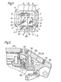
- Figure 1 is a top view of the timepiece according to the invention. It comprises a box 1 in which are mounted an electronic module of which the display 2 can be seen, a plurality 3, 4, 5, 6 and 7 of push buttons and a static sensor 100 which is the subject of the present invention and which will be described in detail later.
- the display 2 which can be formed by a liquid crystal cell, comprises, in addition to the permanent display 8 of the standard time made up of three groups of two digits displaying the hours 9, the minutes 10 and the seconds 11, an auxiliary display 12 which can display for example the day of the week 13, the month 14 and the date 15. Signs 16, permanently fixed and for example transferred under the watch glass signa slow the possible operating modes in which the auxiliary display can be switched.
- the sign AG 1 means “agenda 1" and the sign D the "date”.
- the display of a frame 17 indicates in which mode one is.
- the patent application cited above describes in detail how, by means of the sensor 100, the main display is set to the time, the operating mode is selected and new data is introduced into the auxiliary display.
- FIG. 2 is a section along line A - A through the sensor of Figure 1 and on an enlarged scale.
- the sensor 100 comprises an electrically insulating substrate 30, a first metallization 101, a second metallization 32, connection means 33 between said first and second metallizations, an electrically insulating compensation layer 34, a dielectric 35 and a decorative layer 36.
- second metallization 32 directly carries the electronic means (not shown in FIG. 2) necessary for the operation of the sensor as well as its output terminals (not visible in FIG. 2).
- the insulating substrate 30 constitutes the base of the sensor.
- the choice of its material and its preparation will depend its ability to fulfill the performance expected of it, that is to say, a strong, impact resistance that may occur when wearing the watch.
- sapphire In addition to its high intrinsic resistance, sapphire also has the advantage of withstanding the high temperatures necessary for laying the coatings discussed below. Glass for example, in addition to its great brittleness, would soften in the presence of temperatures of the order of 800 to 1000 ° C.
- the substrate is obtained by sawing in a direction such that the axis C of the hexagonal crystal mesh lies in the plane of said substrate.
- the holes 37 are laser drilled. It should be noted here that this method is one of the only con coming from such a hard and thick material (of the order of a millimeter). It normally results in a diameter d l of a small hole (of the order of 0.1 mm) relative to the thickness d 2. Of the substrate, which is advantageous since it will then be a matter of plugging it by means dielectric 35 as will be explained later. In a preferred version of the invention, the ratio of the thickness d2 to the diameter d l is arranged in such a way that the relation d 2 / d 1 > 4 is satisfied.
- the substrate receives a stabilization heat treatment after which the holes are finally chamfered at 38.
- the scratches which appeared at the birth of the holes are removed by a new running-in.
- the substrate is polished fine on its two large surfaces. It has been found that this polishing is essential for the solidity of the substrate and contributes, by suppressing the incipient fractures which scratches might have, to very clearly improve its impact resistance. To achieve the desired performance and according to experience, the average roughness after polishing will not exceed 0.05 ⁇ m (optical polish).
- FIG. 3 shows an example of the geometry of the first metallization 101 of the substrate, on the outside of the timepiece.
- a conductive paste which may contain, for example, a mixture of palladium, platinum and silver. Whatever paste is chosen, it is essential that it adapts well to the successive covering operations which will be described and above all that it develops excellent adhesion to the polished surface of the substrate.
- the paste known commercially under the name EMCA 7157 A satisfies these requirements well.
- the geometry of this deposit consists of four electrodes of square shape 101.
- the thick layer thus deposited is baked at a temperature between 800 and 1000 ° vs.
- the constitution of the screen-printing screen and the consistency of the paste are chosen so that the thickness of the metallization after baking is between 5 and 15 ⁇ m.
- FIG. 4 shows an example of the geometry of the second metallization 32 of the substrate, on the interior side of the timepiece.
- the deposition takes place, as for the deposition of the electrodes, by screen printing according to the same preferential requirements of paste composition, baking temperature and metallization thickness after baking.
- the same suction is created through the holes 37 but from the outer face of the substrate this time to ensure electrical continuity between the two metal layers.
- the configuration of the second metallization as it appears in FIG. 4 shows various conductors capable of receiving the: electronic means suitable for detecting the position of the finger on the sensor as well as input and output terminals of said sensor. The description will repeat this particular arrangement later.
- the first and second metallizations are not limited to a screen printing process.
- Other known means could be used such as, for example, depositing thin layers under vacuum, the essential being, at least for the second metallization, that the thickness of the conductors is compatible with the ultrasonic connection of gold or aluminum wires (bonding), with tin-lead solder and with bonding using conductive epoxy adhesive.
- a compensation layer 34 which is visible in the section of FIG. 2.
- This electrically insulating layer 34 will be applied by screen printing, baked in the oven at a temperature between 800 and 1000 ° C. Its thickness after firing must be the same as that of the electrodes, that is to say between 5 and 15 m. It should be mentioned here that one could very well deposit the compensation layer 34 before metallization 101. As for the metallization layer, the compensation layer must have excellent adhesion to the polished substrate. The paste known in the trade under the name EMCA 2828 B satisfies this requirement well.
- FIG. 2 also shows that the metallization 101 and the compensation layer 34 are surmounted by a dielectric 35.
- This deposition is carried out by screen printing in at least two passes of an insulating paste.
- this layer must have a suitable relative dielectric constant ⁇ r, of value between 8 and 16, it must also ensure perfect sealing between the front face and the rear face of the sensor.
- the first pass will opt the four metallized holes 37 at the same time as it will cover the entire front face. After drying at around 125 ° C, it still has microscopic pores which will be covered by the second pass in order to protect the electrodes against humidity and ensure perfect opturation of the metallized holes.
- the wafer is baked in the oven at a temperature between 800 and 1000 ° C.
- the thickness of the dielectric after baking will preferably be between 20 and 100 ⁇ m.
- the dielectric must also have good adhesion to the layers on which it is deposited. A paste similar to that used for the compensation layer meets this requirement well.
- FIG. 2 finally shows that the dielectric layer 35 which has just been described is in turn overcome by a decorative layer 36.
- this decorative layer is deposited by screen printing.
- a porcelain enamel which will be fired at a temperature between 770 and 850 ° C.
- This type of enamel much more resistant than baking paint (300 ° C) or glass enamel ( ⁇ 620 ° C), is very hard and resists abrasion well.
- the decorative layer can be applied all at once (one color) or several times (two colors and more).
- An example of decoration in two colors appears in Figure 1 where we find in 40 a white color and in 41 a black decorative pattern which includes a long line embraced by a sign - and by a + sign which mean that the group of digits to be corrected will decrease in value if the finger moves towards the sign - or on the contrary will increase in value if the finger moves towards the + sign.
- the decorative layer 36 also acts as a dielectric layer since it is superimposed on the main dielectric layer 35. It will therefore be important that its thickness after firing (5 to 20 f m approximately), its relative dielectric constant & .r (between 6.5 and 13) and its electrical insulating properties are chosen judiciously so as not to destroy the capacitive effect obtained by the main dielectric.
- a static sensor is therefore now available which, according to a preferred version of the invention, has four capacitive effect electrodes. If the watch wearer touches the decorative layer 36 in the area of an electrode 101 with a finger, the capacitance of the capacitor formed with the mass of the metal case is modified, the finger being part of the mass armature and being separated from the electrode 101 by the dielectric constituted by the layers 35 and 36. It is therefore possible to use this variation in capacity to produce a control signal when the upper face of the sensor is touched by the finger, and thus to produce a sensor capacitive based on this effect.
- this capacitive sensor is arranged in series with a condenser or fixed injection capacity 64 to form a capacitive divider connected on the one hand to ground (armature constituted by the finger) , on the other hand to a terminal 105 of an alternating voltage generator delivering for example a signal at 32 kHz.
- the voltage at the point of connection of the electrode 101 to a frame 103 of the injection capacitor 64 is: representative of the fact that the electrode 101 is subject to a command or not.
- the second metallization 32 serves as conductors for directly carrying the electronic means for detecting the position of the finger on the sensor and of the input and output terminals. tie of said sensor. Said electronic means are described in FIG. 3 of the patent application already cited EP 80107773.6.
- the transcoder 104 and the assembly 113 of this figure are assembled in a single integrated circuit which is placed as indicated in FIG. 4 of the present invention.
- the mass of the circuit is bonded by means of a conductive adhesive to the field 61 itself connected to the supply terminal +.
- the output of the circuit giving the direction of movement of the finger is connected to terminal 109a and the fast and slow outputs intended to influence one or the other display group, depending on whether the finger moves quickly or slowly on the sensor.
- Terminal 62 is made active with a single touch of the finger on the sensor and allows for example the zeroing of seconds or the stopping of an alarm signal.
- Terminal - is the negative input of the power supply and terminal 63, the signal input at 32 kHz.
- the electrodes 101 shown in FIG. 3 are electrically connected to the conductors 103 by the metallized holes 37. These conductors 103 are the same as those which appear under the same reference in FIG. 3 of the application for patent cited.
- the fixed injection capacitors 64 which have been mentioned above, as well as the conductors 103 and 105 are connected to the integrated circuit as illustrated in FIG. 4.
- the terminals of the injection capacitors 64 can be soldered or glued by means of conductive epoxy adhesive to the conductors 103, 105, the metallization 32 serving both as a support and as a fixing for these capacitors.
- These capacitors can be discrete added components, but it would be possible to integrate them entirely or in part according to known methods directly in the circuit 104, 113.
- the integrated circuit 104, 113 is bonded to the various conductors which surround it. Once this operation has been carried out, it is encapsulated according to known techniques. To delimit the encapsulation zone and thus prevent material from reaching unwanted locations, a thick frame 65 (40 to 200 ⁇ m) is deposited on the second metallization 32 by screen printing or by any other technique. suitable.
- Figure 5 is a partial section on an enlarged scale along the free B - B of Figure 1. It shows how the sensor is incorporated in the timepiece.
- the sensor 100 is driven into the middle 80 in the manner of a watch crystal by means of a seal 81. Under the sensor we can see the encapsulated circuit 104, 113.
- the conductors 109a, 124a, 125a, 62 , +, -, 63 presented in FIG. 4 are connected to the circuits 85 for use and display of the watch by means of a flexible multiple connector 82 of the "zebra" type that the sleeve 83 prevents from bending.
- the senor 100 is completely separated from the glass 84.
- the present invention is not limited to this arrangement. Indeed, if the crystal is of the sapphire type (which would therefore meet the requirements posed by the production of the sensor according to the invention), a second zone of this crystal could be used, apart from the first which normally covers the display. , to implement the sensor described here.
- the capacitive sensor is waterproof as usual glass, and like it, withstands the shocks and mechanical, physical and chemical stresses which normally arise in the environment of a wristwatch. We have also seen that the sensor constitutes a compact unit which can be produced in large series, checked for itself and then very simply mounted in the middle of the watch.
Landscapes
- Physics & Mathematics (AREA)
- General Physics & Mathematics (AREA)
- Electric Clocks (AREA)
- Switches That Are Operated By Magnetic Or Electric Fields (AREA)
- Investigating Or Analyzing Materials By The Use Of Electric Means (AREA)
- Electronic Switches (AREA)
Applications Claiming Priority (2)
| Application Number | Priority Date | Filing Date | Title |
|---|---|---|---|
| CH1796/80A CH643978B (fr) | 1980-03-07 | 1980-03-07 | Capteur statique pour piece d'horlogerie. |
| CH1796/80 | 1980-03-07 |
Publications (2)
| Publication Number | Publication Date |
|---|---|
| EP0035740A1 true EP0035740A1 (de) | 1981-09-16 |
| EP0035740B1 EP0035740B1 (de) | 1984-03-07 |
Family
ID=4218793
Family Applications (1)
| Application Number | Title | Priority Date | Filing Date |
|---|---|---|---|
| EP81101528A Expired EP0035740B1 (de) | 1980-03-07 | 1981-03-04 | Kapazitiver Fühler für Zeitgeber und Verfahren zur Herstellung dieses Fühlers |
Country Status (5)
| Country | Link |
|---|---|
| US (1) | US4435090A (de) |
| EP (1) | EP0035740B1 (de) |
| JP (2) | JPS56163480A (de) |
| CH (1) | CH643978B (de) |
| DE (1) | DE3162455D1 (de) |
Families Citing this family (7)
| Publication number | Priority date | Publication date | Assignee | Title |
|---|---|---|---|---|
| US5864518A (en) * | 1996-03-29 | 1999-01-26 | Performance General Corporation | Device and method for analyzing a swimmer's swim stroke |
| WO2000071971A1 (en) | 1999-05-24 | 2000-11-30 | Luxtron Corporation | Optical techniques for measuring layer thicknesses |
| US8964513B2 (en) * | 2005-06-14 | 2015-02-24 | The Swatch Group Research And Development Ltd | Technical or decorative piece associating a transparent material and a silicon based amorphous material and method of manufacturing the same |
| EP1734423B1 (de) * | 2005-06-14 | 2009-10-14 | Asulab S.A. | Montage eines Sensorglases in einem Gehäuse |
| EP1734420B1 (de) * | 2005-06-14 | 2008-11-12 | Montres Rado S.A. | Gehäuse durch ein Glas verschlossen mit nicht sichtbarer Verbindung oder mit Dekorierungsmöglichkeit, und Herstellungsverfahren dafür |
| US8599144B2 (en) * | 2006-07-31 | 2013-12-03 | Cypress Semiconductor Corporation | Grounded button for capacitive sensor |
| US12409633B2 (en) * | 2019-01-07 | 2025-09-09 | Sony Group Corporation | Structure and exterior housing |
Citations (9)
| Publication number | Priority date | Publication date | Assignee | Title |
|---|---|---|---|---|
| US3937049A (en) * | 1973-03-12 | 1976-02-10 | Citizen Watch Co., Ltd. | Monitoring system for digital electronic timepiece |
| FR2281617A1 (fr) * | 1974-08-09 | 1976-03-05 | Seiko Instr & Electronics | Dispositif d'affichage a cristaux liquides |
| FR2331831A1 (fr) * | 1975-11-11 | 1977-06-10 | Seiko Instr & Electronics | Montre electronique |
| US4056699A (en) * | 1975-11-13 | 1977-11-01 | Essex International, Inc. | Touch plate assembly |
| US4136291A (en) * | 1977-05-23 | 1979-01-23 | General Electric Company | Capacitive touch-pad devices with dynamic bias |
| GB2009976A (en) * | 1977-11-29 | 1979-06-20 | Citizen Watch Co Ltd | Electronic timepiece |
| US4161766A (en) * | 1977-05-23 | 1979-07-17 | General Electric Company | Laminated capacitive touch-pad |
| DE2806112A1 (de) * | 1978-02-14 | 1979-08-16 | Bauknecht Gmbh G | Elektrischer beruehrungsschalter |
| GB2027209A (en) * | 1978-07-10 | 1980-02-13 | Gen Electric | Capacitive touchpad sensors |
Family Cites Families (11)
| Publication number | Priority date | Publication date | Assignee | Title |
|---|---|---|---|---|
| CH614831B (de) | 1974-05-08 | Sharp Kk | Auf beruehrung ansprechende schalteinrichtung fuer elektronische armbanduhren. | |
| US4091610A (en) | 1974-05-08 | 1978-05-30 | Sharp Kabushiki Kaisha | Switching mechanism for electronic wristwatch |
| CH599599B5 (de) * | 1974-09-04 | 1978-05-31 | Centre Electron Horloger | |
| JPS5437658Y2 (de) | 1975-01-10 | 1979-11-10 | ||
| US4064688A (en) | 1975-03-06 | 1977-12-27 | Sharp Kabushiki Kaisha | Touch sensitive electrode assembly for solid state wristwatches |
| US4055735A (en) | 1975-10-23 | 1977-10-25 | Honeywell Information Systems Inc. | Touch sensitive device |
| DE2650756A1 (de) | 1975-11-11 | 1977-05-12 | Seiko Instr & Electronics | Elektronische uhr |
| JPS5399980A (en) * | 1977-02-12 | 1978-08-31 | Citizen Watch Co Ltd | Watch with calculator |
| CH626773B (fr) | 1977-11-22 | Ebauches Sa | Dispositif d'actionnement a touche fixe du circuit electronique de commande des fonctions d'une piece d'horlogerie electronique. | |
| US4304976A (en) | 1978-03-16 | 1981-12-08 | Texas Instruments Incorporated | Capacitive touch switch panel |
| US4290052A (en) | 1979-10-26 | 1981-09-15 | General Electric Company | Capacitive touch entry apparatus having high degree of personal safety |
-
1980
- 1980-03-07 CH CH1796/80A patent/CH643978B/fr not_active IP Right Cessation
-
1981
- 1981-02-25 US US06/238,291 patent/US4435090A/en not_active Expired - Fee Related
- 1981-03-04 EP EP81101528A patent/EP0035740B1/de not_active Expired
- 1981-03-04 DE DE8181101528T patent/DE3162455D1/de not_active Expired
- 1981-03-06 JP JP3141681A patent/JPS56163480A/ja active Pending
-
1990
- 1990-02-19 JP JP1990014822U patent/JPH02107097U/ja active Pending
Patent Citations (9)
| Publication number | Priority date | Publication date | Assignee | Title |
|---|---|---|---|---|
| US3937049A (en) * | 1973-03-12 | 1976-02-10 | Citizen Watch Co., Ltd. | Monitoring system for digital electronic timepiece |
| FR2281617A1 (fr) * | 1974-08-09 | 1976-03-05 | Seiko Instr & Electronics | Dispositif d'affichage a cristaux liquides |
| FR2331831A1 (fr) * | 1975-11-11 | 1977-06-10 | Seiko Instr & Electronics | Montre electronique |
| US4056699A (en) * | 1975-11-13 | 1977-11-01 | Essex International, Inc. | Touch plate assembly |
| US4136291A (en) * | 1977-05-23 | 1979-01-23 | General Electric Company | Capacitive touch-pad devices with dynamic bias |
| US4161766A (en) * | 1977-05-23 | 1979-07-17 | General Electric Company | Laminated capacitive touch-pad |
| GB2009976A (en) * | 1977-11-29 | 1979-06-20 | Citizen Watch Co Ltd | Electronic timepiece |
| DE2806112A1 (de) * | 1978-02-14 | 1979-08-16 | Bauknecht Gmbh G | Elektrischer beruehrungsschalter |
| GB2027209A (en) * | 1978-07-10 | 1980-02-13 | Gen Electric | Capacitive touchpad sensors |
Non-Patent Citations (1)
| Title |
|---|
| PATENT ABSTRACTS OF JAPAN, Vol. 2, No. 1, 5 Janvier 1978, page 9498(E-77) & JP-A-52 114 370 (Suwa Seikosha K.K.) (26.09.1977) *Resume, en entier* * |
Also Published As
| Publication number | Publication date |
|---|---|
| DE3162455D1 (en) | 1984-04-12 |
| JPH02107097U (de) | 1990-08-24 |
| JPS56163480A (en) | 1981-12-16 |
| EP0035740B1 (de) | 1984-03-07 |
| CH643978GA3 (de) | 1984-07-13 |
| US4435090A (en) | 1984-03-06 |
| CH643978B (fr) |
Similar Documents
| Publication | Publication Date | Title |
|---|---|---|
| CN1653378A (zh) | 具有太阳电池机构和液晶显示器的装置 | |
| EP2273349B1 (de) | Herstellungsverfahren eines transparenten Elements mit kapazitiven Tasten für ein elektronisches Gerät und dieses Element umfassendes Gerät | |
| EP0035740B1 (de) | Kapazitiver Fühler für Zeitgeber und Verfahren zur Herstellung dieses Fühlers | |
| FR2621420A1 (fr) | Structure a patte de protection pour emploi dans la fabrication de dispositifs de visualisation a cristaux liquides et transistors en couche mince adresses par matrice | |
| US7712954B2 (en) | Device for assembling a touch-type crystal on a case | |
| EP1626316B1 (de) | Uhr mit Lichtleiternuhrenglas | |
| EP1122620B1 (de) | Glas für Uhr mit Funksprechanlage | |
| EP0872783B1 (de) | Zifferblatt im Form einer Solarzelle, insbesondere für eine Uhr | |
| EP4184256A1 (de) | Uhrengehäuse mit einer verkleidungskomponente, auf der ein dünnschichtstapel aufgelagert ist | |
| EP0093633B1 (de) | Substrat für elektronische Schaltung und Verfahren zur Herstellung dieses Substrats | |
| EP1734587B1 (de) | Herstellungsverfahren für ein transparentes Element mit transparenten Elektroden und entsprechendes Element | |
| EP1760557B1 (de) | Uhr mit einem halbleitenden Zifferblatt | |
| EP1055149B1 (de) | Elektrooptische zelle oder elektrochemische photovoltaische zelle und verfahren zu ihrer herstellung | |
| EP1734422A1 (de) | Zusammenbau eines Glases auf ein berührungsempfindliches Gehäuse | |
| CH694351A5 (fr) | Procédé de fabrication de lampes électroluminescentes et appareil réalisé par ce procédé. | |
| JPH0772266A (ja) | 時計用文字板およびその製造方法 | |
| EP1174756B1 (de) | Anzeigeeinheit mit einer elektrooptischen und einer photovoltaischen Zelle | |
| EP0138098A2 (de) | Elektronische Vorrichtung zum Ausarbeiten und Anzeigen einer Information, Verfahren zum Zusammenbauen dieser Vorrichtung und Maschine zur Anwendung des Verfahrens | |
| EP3387494B1 (de) | Tragbarer gegenstand wie armbanduhr oder messinstrument mit solarzeigern | |
| CH701419B1 (fr) | Procédé de fabrication d'un verre à touches capacitives pour un instrument électronique, et instrument comprenant un tel verre. | |
| EP3069200B1 (de) | Elektromechanische oder digitale armbanduhr, die ein zifferblatt umfasst, und herstellungsverfahren eines solchen zifferblatts | |
| EP1042813B1 (de) | Halbleiterschaltung mit einem isolierenden und transparenten substrat | |
| FR2472241A1 (fr) | Procede de fabrication du substrat d'une cellule d'affichage electrochromique et substrat fabrique par ce procede | |
| EP4415057A1 (de) | Transparente solarzelle für ein elektronisches gerät und verfahren zur herstellung einer solchen solarzelle | |
| CH720495A2 (fr) | Cellule solaire transparente, pièce d'horlogerie et procédé de fabrication de ladite cellule solaire |
Legal Events
| Date | Code | Title | Description |
|---|---|---|---|
| PUAI | Public reference made under article 153(3) epc to a published international application that has entered the european phase |
Free format text: ORIGINAL CODE: 0009012 |
|
| AK | Designated contracting states |
Designated state(s): DE FR GB |
|
| 17P | Request for examination filed |
Effective date: 19811028 |
|
| GRAA | (expected) grant |
Free format text: ORIGINAL CODE: 0009210 |
|
| AK | Designated contracting states |
Designated state(s): DE FR GB |
|
| REF | Corresponds to: |
Ref document number: 3162455 Country of ref document: DE Date of ref document: 19840412 |
|
| PLBE | No opposition filed within time limit |
Free format text: ORIGINAL CODE: 0009261 |
|
| STAA | Information on the status of an ep patent application or granted ep patent |
Free format text: STATUS: NO OPPOSITION FILED WITHIN TIME LIMIT |
|
| 26N | No opposition filed | ||
| PGFP | Annual fee paid to national office [announced via postgrant information from national office to epo] |
Ref country code: GB Payment date: 19910225 Year of fee payment: 11 |
|
| PGFP | Annual fee paid to national office [announced via postgrant information from national office to epo] |
Ref country code: FR Payment date: 19910315 Year of fee payment: 11 |
|
| PGFP | Annual fee paid to national office [announced via postgrant information from national office to epo] |
Ref country code: DE Payment date: 19910321 Year of fee payment: 11 |
|
| PG25 | Lapsed in a contracting state [announced via postgrant information from national office to epo] |
Ref country code: GB Effective date: 19920304 |
|
| GBPC | Gb: european patent ceased through non-payment of renewal fee | ||
| PG25 | Lapsed in a contracting state [announced via postgrant information from national office to epo] |
Ref country code: FR Effective date: 19921130 |
|
| PG25 | Lapsed in a contracting state [announced via postgrant information from national office to epo] |
Ref country code: DE Effective date: 19921201 |
|
| REG | Reference to a national code |
Ref country code: FR Ref legal event code: ST |