EP0057505A2 - Verfahren und Vorrichtung zur Behandlung elektrisch leitender Materialien, dazu verwendete Lösungen und auf diese Weise erzeugte Produkte - Google Patents
Verfahren und Vorrichtung zur Behandlung elektrisch leitender Materialien, dazu verwendete Lösungen und auf diese Weise erzeugte Produkte Download PDFInfo
- Publication number
- EP0057505A2 EP0057505A2 EP82300139A EP82300139A EP0057505A2 EP 0057505 A2 EP0057505 A2 EP 0057505A2 EP 82300139 A EP82300139 A EP 82300139A EP 82300139 A EP82300139 A EP 82300139A EP 0057505 A2 EP0057505 A2 EP 0057505A2
- Authority
- EP
- European Patent Office
- Prior art keywords
- matrix
- solution
- conductive
- sem
- fusion
- Prior art date
- Legal status (The legal status is an assumption and is not a legal conclusion. Google has not performed a legal analysis and makes no representation as to the accuracy of the status listed.)
- Granted
Links
Images


Classifications
-
- C—CHEMISTRY; METALLURGY
- C23—COATING METALLIC MATERIAL; COATING MATERIAL WITH METALLIC MATERIAL; CHEMICAL SURFACE TREATMENT; DIFFUSION TREATMENT OF METALLIC MATERIAL; COATING BY VACUUM EVAPORATION, BY SPUTTERING, BY ION IMPLANTATION OR BY CHEMICAL VAPOUR DEPOSITION, IN GENERAL; INHIBITING CORROSION OF METALLIC MATERIAL OR INCRUSTATION IN GENERAL
- C23C—COATING METALLIC MATERIAL; COATING MATERIAL WITH METALLIC MATERIAL; SURFACE TREATMENT OF METALLIC MATERIAL BY DIFFUSION INTO THE SURFACE, BY CHEMICAL CONVERSION OR SUBSTITUTION; COATING BY VACUUM EVAPORATION, BY SPUTTERING, BY ION IMPLANTATION OR BY CHEMICAL VAPOUR DEPOSITION, IN GENERAL
- C23C20/00—Chemical coating by decomposition of either solid compounds or suspensions of the coating forming compounds, without leaving reaction products of surface material in the coating
-
- C—CHEMISTRY; METALLURGY
- C25—ELECTROLYTIC OR ELECTROPHORETIC PROCESSES; APPARATUS THEREFOR
- C25D—PROCESSES FOR THE ELECTROLYTIC OR ELECTROPHORETIC PRODUCTION OF COATINGS; ELECTROFORMING; APPARATUS THEREFOR
- C25D17/00—Constructional parts, or assemblies thereof, of cells for electrolytic coating
- C25D17/10—Electrodes, e.g. composition, counter electrode
- C25D17/14—Electrodes, e.g. composition, counter electrode for pad-plating
-
- C—CHEMISTRY; METALLURGY
- C25—ELECTROLYTIC OR ELECTROPHORETIC PROCESSES; APPARATUS THEREFOR
- C25D—PROCESSES FOR THE ELECTROLYTIC OR ELECTROPHORETIC PRODUCTION OF COATINGS; ELECTROFORMING; APPARATUS THEREFOR
- C25D5/00—Electroplating characterised by the process; Pretreatment or after-treatment of workpieces
- C25D5/18—Electroplating using modulated, pulsed or reversing current
-
- C—CHEMISTRY; METALLURGY
- C25—ELECTROLYTIC OR ELECTROPHORETIC PROCESSES; APPARATUS THEREFOR
- C25D—PROCESSES FOR THE ELECTROLYTIC OR ELECTROPHORETIC PRODUCTION OF COATINGS; ELECTROFORMING; APPARATUS THEREFOR
- C25D5/00—Electroplating characterised by the process; Pretreatment or after-treatment of workpieces
- C25D5/60—Electroplating characterised by the structure or texture of the layers
- C25D5/605—Surface topography of the layers, e.g. rough, dendritic or nodular layers
-
- C—CHEMISTRY; METALLURGY
- C25—ELECTROLYTIC OR ELECTROPHORETIC PROCESSES; APPARATUS THEREFOR
- C25D—PROCESSES FOR THE ELECTROLYTIC OR ELECTROPHORETIC PRODUCTION OF COATINGS; ELECTROFORMING; APPARATUS THEREFOR
- C25D5/00—Electroplating characterised by the process; Pretreatment or after-treatment of workpieces
- C25D5/60—Electroplating characterised by the structure or texture of the layers
- C25D5/623—Porosity of the layers
-
- C—CHEMISTRY; METALLURGY
- C25—ELECTROLYTIC OR ELECTROPHORETIC PROCESSES; APPARATUS THEREFOR
- C25D—PROCESSES FOR THE ELECTROLYTIC OR ELECTROPHORETIC PRODUCTION OF COATINGS; ELECTROFORMING; APPARATUS THEREFOR
- C25D5/00—Electroplating characterised by the process; Pretreatment or after-treatment of workpieces
- C25D5/627—Electroplating characterised by the visual appearance of the layers, e.g. colour, brightness or mat appearance
Definitions
- the present invention relates to fusion processes, apparatus for carrying out such processes and the products of .such processes, and solutions for use in the process.
- the workpiece or matrix may be of a certain form which does not lend itself to the subjection of a particular characteristic-enhancing process; the process may be destructive of the already desirable characteristics of the work-piece; or the treated work-piece while having certain enhanced characteristics may exhibit other reduced characteristics.
- the process employed depends upon the work-piece or matrix to be treated and the characteristics desired.
- coating techniques heat treatment, anodizing, arc spraying, vacuum evaporation, chemical deposition, sputtering, and ion plating are all common processes.
- Non-ferrous metals may be hardened by aging, heat treatment or anodizing.
- Spray coating techniques have not improved corrosion resistance or the physical properties of ferrous materials.
- the other techniques arc-spraying, vacuum evaporation and sputtering have their shortcomings in that the coating deposited is usually thin, the interfacial bond strength is poor, or can only be used to treat small surface areas.
- first conductive chemical element shall refer to the matrix with which fusion is to be accomplished; and the term “chemical element” shall refer to such an element or an alloy thereof; the term “second conductive chemical element or an alloy thereof.” shall refer to the element which is to be fused with the matrix.
- fusion means a penetration by the atoms or molecules of a second element within the solid matrix of a first element or alloy thereof.
- Apparatus which comprises an oscillating circuit for generating a halfwave signal across the output and means for connecting across the output a second chemical element to be fused and the first chemical element to which the second is to be fused.
- Solutions for use in the process and in association, with the apparatus are also provided. These solutions comprise a solution of a conductive chemical of the chemical to be fused in a disassociable form which may be present in the range of 0.10% to 10% by weight and having a pH in the range 0.4 to 14.
- the resistivity of the solution is in the range of 5 to 500 ohms cm, preferably 10 to 80 ohms cm.
- FIG. 1 and 2 these drawings illustrate in general perspective view apparatus in accordance with the invention which is employed to carry out the process of the invention.
- Fig. 1 which exemplifies a solid-to-solid process the number 10 indicates a power supply and 11 an oscillator.
- One side of the oscillator output is connected to an electrode 13 through a holder 12.
- Holder 12 is provided with a rotating chuck and has a trigger switch which controls the speed of rotation of the electrode 13.
- the speed of rotation is variable from 5,000 to 10,000 rpm.
- the electrode 13 is composed of the material to be fused with the matrix.
- the matrix or substrate which is to be subjected to the process and which is to be treated is indicated at 14.
- the matrix is also connected to the other side of the oscillator output by a clamp 15 and line 16.
- the electrode is positively charged and the matrix is negatively charged when the signal is applied.
- Fig. 2 the corresponding components are correspondingly numbered.
- the process employed may be characterized as a liquid to solid process.
- the material to be fused is in the form of a solution, and is held in a reservoir 17.
- reservoir 17 is connected by a tube 18 to an electrode 19.
- Electrode 19 is a plate provided with an insulated handle 20 through which one side of oscillator 11 output is connected. This output is led into a main channel 21 in electrode 19.
- Channel 21 has a series of side channels 22 which open on to the undersurface of electrode 20.
- the flow from reservoir 17 is by gravity or by a pump and may be controlled by a valve such as 23 on the handle 20.
- a permeable membrane such as cotton or nylon.
- the operator passes the rotating electrode 13 in contact with the upper surface of the matrix over the matrix surface at a predetermined speed to apply the electrode; material to the matrix and fuse it therewith.
- both the matrix and the material to be applied have specific resistance characteristics. Thus with each change in either one or both of these materials there is a change in the resistivity of the circuit.
- R 1 the resistance of the electrode
- R 2 the resistance of the matrix
- R 3 the resistance of the circuit of 10 and 11..
- a signal having an amplitude of 3 amps is believed to be the preferred amplitude. If the amplitude is greater decarbonizing or burning of the matrix takes place and below this amplitude hydroxides are formed in the interface.
- Fig. 4 is a schematic diagram of an oscillator circuit used in apparatus in accordance with the present invention.
- a power supply 30 is connected across the input, and across the input a capacitor 31 is connected.
- One side of the capacitor 31 is connected through .
- the LC circuit 32 which comprises a variable inductance coil 33 and capacitor 34 connected in parallel.
- LC circuit 32 is connected to one side of a crystal oscillator circuit comprising crystal 35, inductance 36, NPN transistor 37 and the RC circuit comprised of variable resistance 38 and capacitance 39.
- This oscillator circuit is connected to output 50 through, on one side capacitor 40, and on the other side diode 41, to produce a halfwavesignal across output 50.
- F o depends on the material being treated and the material being applied but it is in the range 400Hz - 35MHz. The frequency, it is believed, will determine the speed of the process.
- the travel speed may be determined by the following form:
- A area to be covered in sq. mm.
- F 1 is the number of discharges per second.
- resistances R 1 and R 2 may be measured by any known means.
- the speed of rotation is also believed to affect the quality of the fusion with a rotation speed of 5,000 rpm the finish is an uneven 200 to 300M finish; with a speed of rotation of 10,000 rpm the finish is a substantially 15M finish.
- the apparatus of Fig. 2 is operated in the same manner as the apparatus of Fig. 1 and the process is essentially the same except for the use of a liquid with a solid electrode.
- the solid to solid process is illustrated by Examples I, II, IIA, III, and IV.
- Atlas A151 01 tool steel was connected to the apparatus of Fig. 1 as the matrix 14 and the electrode 13 was titanium carbide as Kennametal K165.
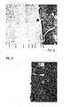
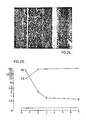
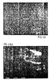
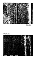
- the polished titanium carbide treated steel was examined by SEM/EPMA nd appeared as shown in Fig. 5.
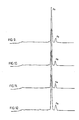
- X-ray spectra were taken at each of the numbered locations indicated in Fig. 1, and they are shown in the graphs which are Figs. 9 through 16 and which correspond to locations 1 through 8, respectively.
- Figs. 9, 10 and 11 give spectra from the parent metal.
- Figs. 12 through 16 show the presence of a small titanium peak which does not change markedly in height as the zone was crossed.
- the approximate width of che zone in which titanium was detected is about 50 m -lthough this dimension varied along the specimen length.
- Fig. 17 is an X-ray spectrum of this layer.
- 1018 Steel was connected to the apparatus of Fig. 1 as the matrix 14 and the electrode 13 was molybdenum, Type Mo 1.
- the steel was 1 ⁇ 2" wide x 1 ⁇ 4" thick x 11 ⁇ 2" long, the molybdenum 1" long x 4 mm diameter.
- the frequency applied was 43.31 KHz. and the speed of electrode rotation approximately 12,000 rpm.
- the surface of the steel was ground to a surface finish of 600 grit.
- the electrode tip was moved manually along the top surface of the steel sample in straight lines adjacent to each other. The process was repeated at 90° to cover the whole surface. Under the optical microscope at x40 magnification small beads of melted and resolidified material were revealed.
- the average KHN of the untreated steel was 188.
- the hardness of the same steel after heating to 900°C and water quenching was 285 (KHN) at 200 gm.
- Example II The same matrix and electrode and procedure as in Example II were followed at a frequency of 30.63 KHz and the same speed of rotation.
- the frequency applied was 26.20 KHz and the speed of electrode rotation was approximately 12,000 rpm.
- tungsten is shown to be fused with the steel matrix.
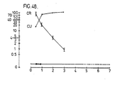
- the results of an electron microscope analysis across the sample indicate the presence of tungsten to a depth of at least 80 um and are shown in Fig. 21 and the following table:
- the hardness of the untreated sample is approximately 188 KHN and after heating to 900°C and quenching was 285 KHN.
- the matrix 14 metal was connected into the circuit as previously described.
- the frequency was determined in accordance with the formula previously set forth and the solution in reservoir 17 applied by movement of the electrode over one surface of the first metal for varying periods of time as determined by Form II.
- the electrode was covered with cotton gauze or nylon. It will be apparent that other materials may be employed. This arrangement also served to limit contamination of the solution when graphite electrodes were employed. They had a tendency to release graphite particles in the course of movement.
- the sample was etched using Nital for steel, the ferrous substrate, and Ammonium Hydrogen Peroxide on the copper, the non-ferrous substrate.
- the surface of the embedding plastic was rendered conductive by evaporating on it approximately 20 um layer of carbon in a vacuum evaporator. This procedure was used to prevent buildup of electrical charges on an otherwise nonconductive material and a consequent instability of the SEM image. Carbon, which does not produce a radiation detectable by the EDX, was used in preference of a more conventional metallic coating to avoid interference of such a coating with the elemental analysis.
- the diameter of analysed volume was calculated for typical elements analysed and was found to be as follows:
- the second conductive chemical element that is the element to be diffused into the matrix
- small quantities of metallic ions of a third metal are also provided.
- the presence of these metal ions is believed to be required as complex forming agents to facilitate fusion.
- Small quantities of organic catalysts such as gum acacia, hydroquinone, animal glue, pepsin, dextrin, licorice, or their equivalents may also be present.
- wetting agents such as sodium lauryl sulphate or its equivalent are usually provided.
- pH varying agents such as ammonium hydroxide or sulphuric acid are usually added to reach an operating pH.
- second chemical conductive element complexing agents which preclude precipitation of the second element. These agents were by way of example citric acid, or sodium pyrophospate, or ethyldiaminetetracetic acid or their equivalents.
- a suitable buffer is also provided in certain solutions, where required.
- the water is always demineralized.
- Atlas A151 1020 steel was connected in the apparatus of Fig. 2 as the matrix 14 and a 10% solution of ammonium-molybdate in water was placed in reservoir 17.
- Example IV The sample of Example IV was subject to a thermal corrosion test. 25% sulphuric acid was applied to the surface for 20 minutes at 325°C without any surface penetration.
- the Mo +6 concentration may be varied from 1.5% to 2.5% by weight; the pH from 7.2 to 8.2 and the resistivity from 17 - 25 ohms cm.
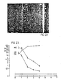
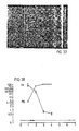
- molybdenum is seen to be fused to a depth of at least 4 um with a surface deposit of approximately 1 um.
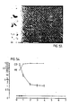
- the photomicrograph Fig. 24, shows the deposition of a substantially uniform layer of molybdenum 1 micron thick of uniform density.
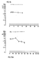
- an SEM/EPMA scan across the interface between the substrate and the applied metal shows molybdenum was present to a depth of at least 10 microns and a molybdenum gradient as set out below in Table.
- the W +6 concentration may vary from 1.6% to 2.5%; the pH may vary from 7.5 to 8.5; and the resistivity may vary from 18 ohms cm to 24 ohms cm.
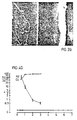
- the sample showed a uniform deposit of tungsten approximately 1 micron thick.
- An SEM/EPMA scan showed fusion of tungsten on copper to a depth of at least 5.0 microns, as can be seen in the Table below and Fig. 28.
- the concentration of tungsten may be varied from 1.6% to 2.5% by wt.; the pH from 7.5 to 8.5; and the conductivity from 18.8 ohms cm to 22.8 ohms cm.
- the Indium concentration may vary from 0.2% to 2.2%; the pH from 1.60 to 1.68; and the resistivity from 48.8 ohms cm to 54.8 ohms cm.
- Example IX The solution of Example IX was employed and applied to a steel matrix:
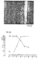
- Fig. 35 shows a solid deposit of nickel of uniform density approximately 1.5 um thick. As shown in the following Table and Fig. 36 an SEM/EPMA scan across the interface between the matrix and the nickel layer shows nickel to be fused to a depth of at least 4 um.
- the nickel concentration may vary from 2% to 10%; pH from 3.10 to 3.50; and resistivity from 17 ohms cm to 26 ohms cm.
- Example XI The same solution as was formulated for Example XI was prepared and applied to a steel matrix:
- the nickel layer is continuous and substantially uniform in thickness being about 1.5 um thick.
- nickel is shown to be fused to a depth of at least 3 um.
- the pH may be varied from 3.70 to 11; the concentration of Au +3 ions may vary from 0.1% to 0.5% by weight; and the resistivity from 40 ohms cm to 72 ohms cm.
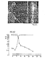
- An SEM/EPMA scan across the interface indicated fusion of gold to a depth of at least 3 um as shown on the Table below and Fig. 40.
- An SEM/EPMA scan across the interface indicated fusion of gold to a depth of at least 4.0 um as shown on the table below and Fig. 42.
- the pH may be varied from 0.6 to 1.0; the concentration of Cr +6 ions may vary from 3% to 20% by weight; and the resistivity from 11 ohms cm to 14 ohms cm.
- An SEM/EPMA scan across the interface indicated fusion of chromium to a depth of at least 3.0 um as shown on the table below and Fig. 44.
- An SEM/EPMA scan across the interface indicated fusion of chromium to a depth of at least 5.0 um as shown on the table below and Fig. 46.
- the pH may be varied from 2.5 to 3.5; the concentration of Cr +3 ions may vary from 1.8% to 5% by weight; and the resistivity from 16 ohms cm to 20 ohms cm.
- An SEM/EPMA scan across the interface indicated fusion of chromium to a depth of at least 3.0 um as shown on the Table below and Fig. 48.
- An SEM/EPMA scan across the interface indicated fusion of chromium to a depth of at least 3.0 um as shown on the table below and Fig. 50.
- the pH may be varied from 10 to 10.2; the concentration of Cd +2 ions may vary from 0.2% to 0.5% by weight; and the resistivity from 28 ohms cm to 35 ohms cm.
- Example XX Example XX
- the pH may be varied from 3.2 to 3.5; the concentration of Cd +2 ions may vary from 1% to 4% by weight; and the resistivity from 45 ohms cm to 55 ohms cm.
- An SEM/EPMA scan across the interface indicated fusion of cadmium to a depth of at least 4 um as shown on the Table below and Fig. 54.
- the pH may be varied from 11.2 to 12.7; the concentration of Sn +2 ions may vary from 2% to 5% by weight; and the resistivity from 6.2 ohms cm to 10.3 ohms cm.
- An SEM/EPMA scan across the interface indicated fusion of tin to a depth of at least 4 um as shown on the table below and Fig. 56.
- the pH may be varied from 9 to 9.7; the concentration of Sn +2 ions may vary from 0.4% to 1% by weight; and the resistivity from 30 ohms cm to 36 ohms cm.
- An SEM/EPMA scan across the interface indicated fusion of tin to a depth of at least 5 um as shown on the Table below and Fig. 58.
- An SEM/EPMA scan across the interface indicated fusion of tin to a depth of at least 2 um as shown on the table below and Fig. 60.
- the pH may be varied from 4.5 to 6.5; the concentration of Co+2 ions may vary from 2% to 6% by weight; and the resistivity from 25 ohms cm to 30 ohms cm.
- the pH may be varied from 11.2 to 11.7; the concentration of Ag +l ions may vary from 1% to 3% by weight;. and the resistivity from 8 ohms cm to 13 ohms cm.
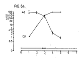
- An SEM/EPMA scan across the interface indicated fusion of silver to a depth of at least 3 um as shown on the Table below and Fig. 64.
- the pH may be varied from 1.5 to 2; the concentration of Ag +l ions may vary from 0.5% to 2.5% by weight; and the resistivity from 6 ohms cm to 12 ohms cm.
- An SEM/EPMA scan across the interface indicated fusion of silver to a depth of at least 2.00 um as shown on the Table below and Fig. 66.
- tin, gold and silver with their inherent excellent conductivity characteristics may be employed in electrical applications and circuits may be fused on other substrates.
- the anti-corrosion characteristics of tin, gold, silver, nickel, chromium, cadmium, molybdenum and tungsten are also useful. And the application of those metals to ferrous or non-ferrous substrates will enhance their anti-corrosion behaviour.
- Chromium, nickel, silver, gold or tin have the . capability of imparting an elegant appearance to the matrix. Chromium, molybdenum, tungsten, titanium and cobalt impart a surface hardness to the matrix.
- Indium imparts strength to the matrix, and also serves as anti-galling agent.
- a molybdenum treated ferrous or non-ferrous matrix has improved friction-wear and high temperature resistance characteristics. It is also useful as a dielectric coating.
- a cadmium fused matrix as well as having enhanced corrosion resistance characteristics can also serve as an anti-fouling agent for ship hull treatment.
- Silver fused matrices are all useful as a reflecting medium.
Landscapes
- Chemical & Material Sciences (AREA)
- Organic Chemistry (AREA)
- Engineering & Computer Science (AREA)
- Chemical Kinetics & Catalysis (AREA)
- Materials Engineering (AREA)
- Metallurgy (AREA)
- Electrochemistry (AREA)
- General Chemical & Material Sciences (AREA)
- Mechanical Engineering (AREA)
- Electroplating Methods And Accessories (AREA)
- Other Surface Treatments For Metallic Materials (AREA)
- Chemically Coating (AREA)
- Electroplating And Plating Baths Therefor (AREA)
Priority Applications (1)
| Application Number | Priority Date | Filing Date | Title |
|---|---|---|---|
| AT82300139T ATE36014T1 (de) | 1981-01-13 | 1982-01-12 | Verfahren und vorrichtung zur behandlung elektrisch leitender materialien, dazu verwendete loesungen und auf diese weise erzeugte produkte. |
Applications Claiming Priority (4)
| Application Number | Priority Date | Filing Date | Title |
|---|---|---|---|
| US22476281A | 1981-01-13 | 1981-01-13 | |
| US31967281A | 1981-11-09 | 1981-11-09 | |
| US319672 | 1981-11-09 | ||
| US224762 | 1994-04-08 |
Publications (3)
| Publication Number | Publication Date |
|---|---|
| EP0057505A2 true EP0057505A2 (de) | 1982-08-11 |
| EP0057505A3 EP0057505A3 (en) | 1982-09-22 |
| EP0057505B1 EP0057505B1 (de) | 1988-07-27 |
Family
ID=26918998
Family Applications (1)
| Application Number | Title | Priority Date | Filing Date |
|---|---|---|---|
| EP82300139A Expired EP0057505B1 (de) | 1981-01-13 | 1982-01-12 | Verfahren und Vorrichtung zur Behandlung elektrisch leitender Materialien, dazu verwendete Lösungen und auf diese Weise erzeugte Produkte |
Country Status (14)
| Country | Link |
|---|---|
| EP (1) | EP0057505B1 (de) |
| KR (1) | KR830009257A (de) |
| AU (1) | AU7944882A (de) |
| BR (1) | BR8200154A (de) |
| CA (1) | CA1187035A (de) |
| DD (1) | DD202312A5 (de) |
| DE (1) | DE3278814D1 (de) |
| DK (1) | DK11082A (de) |
| FI (1) | FI820063L (de) |
| GR (1) | GR75834B (de) |
| IL (1) | IL64706A0 (de) |
| NO (1) | NO820075L (de) |
| PL (1) | PL234879A1 (de) |
| PT (1) | PT74270B (de) |
Family Cites Families (1)
| Publication number | Priority date | Publication date | Assignee | Title |
|---|---|---|---|---|
| US3802854A (en) * | 1973-03-19 | 1974-04-09 | Akad Wissenschaften Ddr | Process for forming magnetic metal deposits on a flexible base for use as information data carrier product thereof |
-
1982
- 1982-01-04 IL IL64706A patent/IL64706A0/xx unknown
- 1982-01-08 FI FI820063A patent/FI820063L/fi not_active Application Discontinuation
- 1982-01-11 CA CA000393920A patent/CA1187035A/en not_active Expired
- 1982-01-12 EP EP82300139A patent/EP0057505B1/de not_active Expired
- 1982-01-12 GR GR66993A patent/GR75834B/el unknown
- 1982-01-12 PT PT74270A patent/PT74270B/pt unknown
- 1982-01-12 NO NO820075A patent/NO820075L/no unknown
- 1982-01-12 DE DE8282300139T patent/DE3278814D1/de not_active Expired
- 1982-01-12 AU AU79448/82A patent/AU7944882A/en not_active Abandoned
- 1982-01-13 KR KR1019820000119A patent/KR830009257A/ko not_active Withdrawn
- 1982-01-13 BR BR8200154A patent/BR8200154A/pt unknown
- 1982-01-13 DD DD82236711A patent/DD202312A5/de unknown
- 1982-01-13 DK DK11082A patent/DK11082A/da not_active Application Discontinuation
- 1982-01-29 PL PL23487982A patent/PL234879A1/xx unknown
Also Published As
| Publication number | Publication date |
|---|---|
| PT74270B (en) | 1986-01-10 |
| GR75834B (de) | 1984-08-02 |
| DD202312A5 (de) | 1983-09-07 |
| IL64706A0 (en) | 1982-03-31 |
| PT74270A (en) | 1982-02-01 |
| KR830009257A (ko) | 1983-12-19 |
| EP0057505B1 (de) | 1988-07-27 |
| FI820063A7 (fi) | 1982-07-14 |
| PL234879A1 (en) | 1983-05-09 |
| AU7944882A (en) | 1982-07-22 |
| FI820063L (fi) | 1982-07-14 |
| EP0057505A3 (en) | 1982-09-22 |
| DK11082A (da) | 1982-07-14 |
| DE3278814D1 (en) | 1988-09-01 |
| BR8200154A (pt) | 1982-11-03 |
| CA1187035A (en) | 1985-05-14 |
| NO820075L (no) | 1982-07-14 |
Similar Documents
| Publication | Publication Date | Title |
|---|---|---|
| Aghajani et al. | Electro spark deposition of WC–TiC–Co–Ni cermet coatings on St52 steel | |
| CZ298798A3 (cs) | Elektrolytický způsob čištění a potahování elektricky vodivých povrchů | |
| Khaled et al. | Electrochemical study of laser nitrided and PVD TiN coated Ti–6Al–4V alloy: the observation of selective dissolution | |
| Vykhodtseva et al. | Composition, structure, and corrosion–electrochemical properties of chromium coatings deposited from chromium (III) electrolytes containing formic acid and its derivatives | |
| DE10203730A1 (de) | Verfahren zur Abscheidung von metallfreien Kohlenstoffschichten | |
| US4764654A (en) | Process and apparatus for treating electrically conductive matrices and products produced by the process | |
| US4840711A (en) | Process for the fusion of one element into a second element | |
| Oulladj et al. | Preparation and properties of electroless Ni–Zn–P alloy films | |
| EP0056331B1 (de) | Verfahren und Vorrichtung zur Behandlung elektrisch leitender Materialien und damit erhaltene Produkte | |
| KR20010015609A (ko) | 전기 도금 공정 | |
| EP0057505A2 (de) | Verfahren und Vorrichtung zur Behandlung elektrisch leitender Materialien, dazu verwendete Lösungen und auf diese Weise erzeugte Produkte | |
| EP0402368A1 (de) | Cvd-verfahren zum niederschlagen einer schicht auf einer elektrisch leitfähigen dünnschichtstruktur. | |
| EP0066347B1 (de) | Elektrolysebad zur Abscheidung und Verbindung metallischer Überzüge auf metallischen Substraten | |
| US3445351A (en) | Process for plating metals | |
| Van Ooij et al. | The role of electron spectroscopy in the evolution of long‐range industrial R&D illustrated by AES studies in adhesion, catalysis and corrosion | |
| JPS6138272B2 (de) | ||
| Eltoum | Electroless and corrosion of nickel, phosphorus, tungsten alloy | |
| US4566992A (en) | Solutions for the fusion of one metal to another | |
| Tytarenko et al. | Structure and properties of composite nickel coatings deposited by means of programmable pulsed current under laser irradiation | |
| Hosseini et al. | Electrodeposition and mechanical properties of Ni-WB composites from tartrate bath | |
| Yao et al. | The Research on Coating of Electroless Ni-WP Ternary Alloys | |
| Kalaivani et al. | Pulse reverse plating of silver on silver alloy | |
| Morks et al. | Microstructure, corrosion behavior, and microhardness of plasma-sprayed W–Ni composite coatings | |
| Suryanto et al. | Pulse electrodeposited nickel molybdenum | |
| Wang et al. | Electrochemical behavior of electroless Ni-P-SiC nano-composite coatings |
Legal Events
| Date | Code | Title | Description |
|---|---|---|---|
| PUAI | Public reference made under article 153(3) epc to a published international application that has entered the european phase |
Free format text: ORIGINAL CODE: 0009012 |
|
| PUAL | Search report despatched |
Free format text: ORIGINAL CODE: 0009013 |
|
| AK | Designated contracting states |
Designated state(s): AT BE CH DE FR GB IT NL SE |
|
| AK | Designated contracting states |
Designated state(s): AT BE CH DE FR GB IT NL SE |
|
| 17P | Request for examination filed |
Effective date: 19830321 |
|
| GRAA | (expected) grant |
Free format text: ORIGINAL CODE: 0009210 |
|
| AK | Designated contracting states |
Kind code of ref document: B1 Designated state(s): AT BE CH DE FR GB IT LI NL SE |
|
| PG25 | Lapsed in a contracting state [announced via postgrant information from national office to epo] |
Ref country code: SE Effective date: 19880727 Ref country code: NL Effective date: 19880727 Ref country code: LI Effective date: 19880727 Ref country code: AT Effective date: 19880727 Ref country code: CH Effective date: 19880727 |
|
| REF | Corresponds to: |
Ref document number: 36014 Country of ref document: AT Date of ref document: 19880815 Kind code of ref document: T |
|
| REF | Corresponds to: |
Ref document number: 3278814 Country of ref document: DE Date of ref document: 19880901 |
|
| ITF | It: translation for a ep patent filed | ||
| REG | Reference to a national code |
Ref country code: CH Ref legal event code: PL |
|
| ET | Fr: translation filed | ||
| NLV1 | Nl: lapsed or annulled due to failure to fulfill the requirements of art. 29p and 29m of the patents act | ||
| PLBE | No opposition filed within time limit |
Free format text: ORIGINAL CODE: 0009261 |
|
| STAA | Information on the status of an ep patent application or granted ep patent |
Free format text: STATUS: NO OPPOSITION FILED WITHIN TIME LIMIT |
|
| 26N | No opposition filed | ||
| PGFP | Annual fee paid to national office [announced via postgrant information from national office to epo] |
Ref country code: BE Payment date: 19890731 Year of fee payment: 8 |
|
| PG25 | Lapsed in a contracting state [announced via postgrant information from national office to epo] |
Ref country code: BE Effective date: 19900131 |
|
| BERE | Be: lapsed |
Owner name: METAFUSE LTD Effective date: 19900131 |
|
| ITTA | It: last paid annual fee | ||
| PGFP | Annual fee paid to national office [announced via postgrant information from national office to epo] |
Ref country code: GB Payment date: 19910627 Year of fee payment: 10 |
|
| PGFP | Annual fee paid to national office [announced via postgrant information from national office to epo] |
Ref country code: FR Payment date: 19910704 Year of fee payment: 10 |
|
| PG25 | Lapsed in a contracting state [announced via postgrant information from national office to epo] |
Ref country code: GB Effective date: 19920112 |
|
| GBPC | Gb: european patent ceased through non-payment of renewal fee | ||
| REG | Reference to a national code |
Ref country code: GB Ref legal event code: 728C |
|
| PG25 | Lapsed in a contracting state [announced via postgrant information from national office to epo] |
Ref country code: FR Effective date: 19940228 |
|
| REG | Reference to a national code |
Ref country code: FR Ref legal event code: ST |
|
| REG | Reference to a national code |
Ref country code: GB Ref legal event code: 728R |
|
| REG | Reference to a national code |
Ref country code: FR Ref legal event code: R1 |
|
| PGFP | Annual fee paid to national office [announced via postgrant information from national office to epo] |
Ref country code: DE Payment date: 19950306 Year of fee payment: 14 |
|
| REG | Reference to a national code |
Ref country code: FR Ref legal event code: D5 |
|
| PG25 | Lapsed in a contracting state [announced via postgrant information from national office to epo] |
Ref country code: DE Effective date: 19961001 |
|
| PG25 | Lapsed in a contracting state [announced via postgrant information from national office to epo] |
Ref country code: FR Effective date: 19920131 |