EP0063624A1 - Method and circuit for the discrimination of alpha and beta particles - Google Patents
Method and circuit for the discrimination of alpha and beta particles Download PDFInfo
- Publication number
- EP0063624A1 EP0063624A1 EP81103119A EP81103119A EP0063624A1 EP 0063624 A1 EP0063624 A1 EP 0063624A1 EP 81103119 A EP81103119 A EP 81103119A EP 81103119 A EP81103119 A EP 81103119A EP 0063624 A1 EP0063624 A1 EP 0063624A1
- Authority
- EP
- European Patent Office
- Prior art keywords
- time
- output
- pulse
- gate
- detector
- Prior art date
- Legal status (The legal status is an assumption and is not a legal conclusion. Google has not performed a legal analysis and makes no representation as to the accuracy of the status listed.)
- Granted
Links
Images


Classifications
-
- G—PHYSICS
- G01—MEASURING; TESTING
- G01T—MEASUREMENT OF NUCLEAR OR X-RADIATION
- G01T1/00—Measuring X-radiation, gamma radiation, corpuscular radiation, or cosmic radiation
- G01T1/36—Measuring spectral distribution of X-rays or of nuclear radiation spectrometry
- G01T1/38—Particle discrimination and measurement of relative mass, e.g. by measurement of loss of energy with distance (dE/dx)
Definitions
- the invention relates to a method and a circuit arrangement for discriminating pulses generated by ⁇ and / or ⁇ emitters according to the preamble of claim 1.
- Detector pulses are generated in a detector according to patent application P 3o o3 9o9.9-33, the leading edges of which rise linearly in a first approximation in a time in the nanosecond range and at the same time have very different slopes for ⁇ -pulses and ⁇ -pulses.
- the invention is based on the object of developing a method and a circuit arrangement for carrying it out which makes it possible to identify the detector pulses emitted at the output of the one detector as unambiguously as ⁇ or ⁇ pulses regardless of the pulse height determined by the particle energy.
- the advantages achieved by the invention are, in particular, that a predetermined detection limit is achieved with a significantly shorter measurement time, or that a significantly increased sensitivity to detection can be achieved with an unreduced measurement time, that, in particular in the case of ⁇ - ⁇ mixed samples, a substantial reduction in the measurement error of the x- Pulse rate occurs that the temporal resolution is significantly increased, and that the separation of the ⁇ and ⁇ pulses is made possible with high accuracy.
- the leading edges of ⁇ and ⁇ pulses run approximately in a straight line and have very different slopes ⁇ and ⁇ .
- the increase U ⁇ of an ⁇ pulse is approximately twice as large as the increase U ⁇ of a ⁇ pulse in this area.
- the use of the difference quotients ⁇ U ⁇ / ⁇ t and ⁇ U ⁇ / At as a criterion for discrimination is therefore only possible in the first 2o to 3o ns.
- a corresponding time discrimination of the detector pulses is therefore carried out.
- ⁇ and ⁇ pulses reach very different amplitudes A, namely ⁇ U ⁇ ⁇ 2 ⁇ U ⁇ , so that due to amplitude discrimination that is subordinate to time discrimination, the detector pulses in the vast majority of events clearly as ⁇ or ⁇ pulses are identifiable. A few percent of events cannot be clearly assigned and is counted as the "quality" of the measurement.
- FIG. 2 shows the block diagram of a discriminator for performing the method.
- detector pulses 2 are generated, which are used to compensate for signal attenuations caused by the construction of the detector, with a first integrated into detector 1
- Amplifier 3 are amplified, which has an output impedance of 50 ohms.
- the output A of the detector 1 is connected to a first comparator 7 with a predetermined first threshold S 1 and to a second comparator 8 with a predetermined second threshold S 2 > S 1 .
- the non-inverting output of the first comparator 7 is connected via a digital delay element 9, the inverting output of the second comparator 8 directly to a start circuit lo, which only triggers the start circuit lo when the amplitudes A of the detector pulse 2 exceed the second threshold S2.
- the output of the start circuit lo is switched to a level adjustment 11, which converts a change in the input signal from “O” to "1” into a voltage change from O to -5 volts.
- a gate time pulse generator 12 connected downstream of the level adjustment 11 generates gate time pulses 13 of predetermined, constant pulse width t 3 lying in the nanosecond range.
- the output of the gate time pulse generator 12 is connected to the control input of the electronic switch 6 which can be controlled by the gate time pulse 13 during the time t 1 .
- the time delay t 2 of the detector pulse is determined by the time delays of the components required for signal processing and is set by the delay line 4.
- the leading edge 14 of the gate time pulse 13 lies immediately before the delay time t 2 expires.
- the electronic switch 6 is blocked by the trailing edge 15 of the gate time pulse 13.
- the trailing edge 15 thus also determines the end of the time t provided for the time discrimination and stops the rising of the leading edge 5 of the detector pulse 2 at an amplitude value A ⁇ , A ⁇ .
- the electronic switch 6 is followed by a pulse shaper 16, which converts the signal voltages of the time-discriminated detector pulse 2 corresponding to the amplitudes A ⁇ , A ⁇ into an electrical charge of a capacitor and stretches the peak-shaped maximum value 17 of the amplitudes A ⁇ , A ⁇ obtained by the time discrimination .
- the output of the pulse shaper 16 is connected via a second amplifier 18 to the inputs of a third comparator 19 with a predetermined third threshold S 3 > S 2 and a fourth comparator 2o with a predetermined fourth threshold S 4 > S 3 .
- the inverting output of the third comparator 19 is on a fourth memory 21, the inverting.
- the output of the fourth comparator 2o is connected to a fifth memory 22.
- the outputs of the fourth memory 21 and the fifth memory 22 are connected to an evaluation logic 23 which sorts the time and amplitude-discriminated detector pulse into ⁇ signals, ⁇ signals and ⁇ or ⁇ signals.
- the evaluation logic 23 is followed by a first counter 24 for ⁇ signals, a second counter 25 for ⁇ signals and a third counter 26 for ⁇ or ⁇ signals.
- the inverting output of the first comparator 7 is followed by a timer 27, the output of which is connected to the evaluation logic 23.
- the timer At the end of the measuring time, the timer generates a read pulse for transferring the contents of the fourth memory 21 or the fifth memory 22 via the evaluation logic 23 into one of the counters 24, 25, 26.
- the inverting output of the first comparator 7 is followed by a reset logic 28, the second input is connected to the output of the timer 27 and its output is connected to the reset inputs of the memories, the reset logic 28, the start circuit 10 and the fourth and fifth memories 21, 22.
- Each of the stores consists of a bistable flip-flop.
- FIG. 3 shows the circuit diagram of the comparators, the memories, the start circuit 10, the evaluation logic 23 and the reset logic 28.
- the start circuit lo generates only at the second threshold S 2 exceeding signal amplitudes Ay, A ⁇ at its output 3o a signal triggering the level adjustment 11.
- the starting circuit 10 consists of a second bistable multivibrator 31, a third bistable multivibrator 32, a second NAND gate 33 and a third NAND gate 34.
- the second bistable multivibrator 31 is connected downstream of the second NAND gate 33, the first input of which is connected to the output of the digital delay element 9 and the second input of which is connected to the inverting output of the second comparator 8.
- the non-inverting output 35 of the second flip-flop 31 is connected to the first input of the third NAND gate 34, the second input of which is connected to the non-inverting output of the second comparator 8.
- the output of the third NAND gate 34 is followed by the third bistable multivibrator 32, whose inverting output 3o is connected to the level adjustment 11.
- the level adjustment 11 consists essentially of a pnp transistor 36 whose base lo at the output of the starting circuit 3o, whose emitter auf.eine positive voltage of 5 volts, and the collector to a ne g a- tive voltage of 5 volts is switched.
- the output of the level adjustment 11 is connected via the point C of the circuit to the input of a sixth bistable multivibrator 37 of the gate time pulse generator 12 shown in FIG. 4.
- the inverting output 38 of the flip-flop 37 is connected via a driver stage 39 to the control electrode of the electronic switch 6 designed as a field effect transistor 40.
- the non-inverting output 41 of the sixth bistable multivibrator 37 is fed back to its reset input via a delay element 42 which determines the opening time t 3 of the FET 40.
- the falling edge of the control signal generated by the level adjustment 11 triggers the sixth bistable multivibrator 37, whose inverting output 38 switches from -5 volts to 0 volts and thereby generates the leading edge 14 of the gate time pulse 13 shown in FIG. 1.
- the non-inverting output 41 goes from 0 to -5 volts.
- This signal is fed back to the reset input by the delay element 42, delayed by the time t 3 , and generates the trailing edge 15 of the gate time pulse 13, which determines the opening time t 3 of the electronic switch 6.
- a downstream integrating element 44 causes a temporal expansion of the peak-shaped maximum value 17 of the pulse amplitudes AO (, A ⁇ obtained by the time discrimination, which transmit the second amplifier 18 and the point B of the circuit via the point E of the circuit to the part of the circuit arrangement which effects the amplitude discrimination will.
- the non-inverting output 45 of the fourth memory 21 designed as a bistable multivibrator is connected to a first input of a first AND gate 46, the inverting output 47 is connected to a first input of a second AND gate 48, the second input of which is connected to the non-inverting output 49 of the fifth Memory 22 is switched.
- the inverting output 50 of the fifth memory 22 is connected to a first input of a third AND gate 51.
- the output of the second AND gate 48 is connected to a first input of a fourth AND gate 52.
- the second input of the first AND gate 46, the second input of the third AND gate 51 and the second input of the fourth AND gate 52 are connected to the output of the timer 27.
- the output of the first AND gate 46 is on a second counter 25 counting the B events
- the output of the third AND gate 51 is on a first counter 24 counting the ⁇ events
- the output of the fourth AND gate 52 is on a third counter 26, which counts neither the .alpha. or .beta.
- the first to fourth AND gates 46, 48, 51, 52 form the evaluation logic 23.
- the inverting output of the first comparator 7 is followed by a first monostable multivibrator 53 and this is followed by a second monostable multivibrator 54; the two flip-flops form the timer 27.
- the output of the timer 27 is connected to the input of a first bistable flip-flop 55, the inverting output 56 of which is connected to the first input of a first NAND gate 57.
- the second input of the first NAND gate 57 is connected to the inverting output of the first comparator 7.
- the output of the first NAND gate 57 is connected to the reset inputs of the first to fifth bistable flip-flops 55, 31, 32, 21, 22.
- the first bistable multivibrator 55 and the first NAND gate 57 form the reset logic 28.
- the second input of the second NAND gate 33 which is connected to the inverting output of the second comparator 8, remains at '1', so that the output of the second NAND gate 33 and thus the input of the second bistable multivibrator 31 and its non-inverting Output changes from '1' to '0'.
- the first input of the third NAND gate 34 thus goes to '0', the second input remains to 'O' and the output remains to '1', so that the inverting output of the third memory 32 remains at 'O' and the start circuit lo does not initiate a measurement process with time and amplitude discrimination.
- the inverting output of the first comparator 7 changes simultaneously from '1' to '0'.
- the falling edge triggers the first monostable multivibrator 53 and this, with a time delay, triggers a second monostable multivibrator 54 of the timing element 27, the output of which is connected to the first input of the first AND gate 46 of the evaluation logic 23.
- the second input of the first AND gate 46 is at '1', so that only the second counter 25 connected downstream of the first AND gate 38 for ⁇ signals receives a counting pulse from the '1' signal of the timing element 27.
- the level adjustment 11 converts the trigger pulse of the start circuit lo into a voltage change from 0 volts to -5 volts.
- This falling edge sets the sixth bistable multivibrator 37, which operates with an operating voltage of 0 and -5 volts.
- the inverting output 38 changes from -5 volts to 0 volts and generates the front edge 14 of the gate time pulse 13 that opens the switch 6 (see FIG. 1).
- the non-inverting output 41 resets the flip-flop after a time t 3 of approximately 3ns which can be determined by the delay element 42.
- the trailing edge 15 of the gate time pulse 13, which closes the switch 6, is generated.
- the time-discriminated detector signal is now discriminated in amplitude to determine the amplitude.
- A> S 4 unique ⁇ signal The inverting output of the fourth comparator 20 goes from '1' to '0', the inverting output 50 of the fifth memory 22 changes from '0' to '1'. Since the threshold S 1 has been exceeded, the first inputs of the first, third and fourth AND gates 46, 51, 52 are set to '1' via the output of the timing element 27. The output of the third AND gate thus goes to '1' and the first counter 24 counts an ⁇ pulse. The second and third counters 25, 26 do not receive a count pulse since the second inputs of the first and fourth AND gates 46, 52 connected upstream of the counter are at '0'.
- the positive pulse of the second monostable multivibrator 54 is thus used as a read signal for the fourth and fifth memories 21; 22 used.
- the time discrimination is running.
- the trailing edge of the pulse at the output of the second monostable multivibrator 54 ends the reading process of the fourth and fifth memories 21, 22 and simultaneously sets the inverted output 56 of the first bistable multivibrator 55 and the first input of the first NAND gate 57 to '1'. If its other input, which is connected to the inverting output of the first comparator 7, is also at '1', the output of the first NAND gate 57 goes to '0'.
- the first to fifth memories 55, 31, 32, 21, 22 are reset to a predetermined starting position and prepared for a new measurement.
- the combination of the output 56 of the first memory 55 with the inverting output of the first comparator 7 ensures that the reset pulse is only given to the memory if it is certain that the threshold S 1 of the first comparator 7 has not been exceeded, that is to say, itself no detector signal 2 is on the line.
- the pulse length of an ⁇ or ⁇ pulse is approx. 150 ns, the time required for a measurement is approx. 1.2 ⁇ s. Because of the statistical distribution of the pulses, one or more additional pulses can occur during a measurement. As soon as a measuring process is initiated by setting the third memory 32, further ⁇ or ⁇ pulses are therefore suppressed by the circuit until after the reset pulse their readiness for measurement is restored.
- Precondition for an exact measurement is that the reset pulse falls in time between two measurement signals, so that the measuring device is ready for operation when a detector signal 2 is received.
- the links in the circuit arrangement ensure that the time discrimination always begins with the rising front edge of the detector signal 2.
Landscapes
- Physics & Mathematics (AREA)
- Spectroscopy & Molecular Physics (AREA)
- Health & Medical Sciences (AREA)
- Life Sciences & Earth Sciences (AREA)
- General Physics & Mathematics (AREA)
- High Energy & Nuclear Physics (AREA)
- Molecular Biology (AREA)
- Manipulation Of Pulses (AREA)
- Measurement Of Radiation (AREA)
- Measurement Of Unknown Time Intervals (AREA)
Abstract
Durch α und β-Teilchen enthaltende Proben werden mit einem Detektor nach Patentanmeldung P 3 003 909.9-33 Detektorimpulse erzeugt, deren Vorderflanken während einer vorbestimmten Zeit teilchenspezifisch annähernd konstant ansteigen und die von α-Teilchen erzeugten Impulse eine erste Steigung α aufweisen, die wesentlich größer ist als eine zweite Steigung β der von β-Teilchen erzeugten Impulse. Dieses von der Energie der Teilchen weitgehend unabhängige physikalische Phänomen wird zur Diskriminierung verwendet. Dabei wird der lineare Anfangsbereich der Vorderflanke des Detektorimpulses im Nanosekundenbereich zeitdiskriminiert. Während der durch die Zeitdiskriminierung vorbestimmten Zeit erreichen die Detektorimpulse von α-Teilchen wesentlich höhere Amplitudenwerte als die von β-Teilchen verursachten Detektorimpulse. Die Amplitude des zeitdiskriminierten Detektorimpulses wird durch Amplitudendiskrimination bestimmt und in Triggerimpulse umgesetzt, die einen ersten Zähler für eindeutige α-Ereignisse oder einen zweiten Zähler für eindeutige β-Ereignisse triggern. Bei einem sehr kleinen Teil der Detektorimpulse, dessen durch Zeitdiskriminierung gewonnene Amplituden nicht eindeutig α- oder β-Ereignissen zuzuordnen sind, wird ein dritter Zähler getriggert, der die Güte der Messung anzeigt.Samples containing α and β particles are used to generate detector pulses with a detector according to patent application P 3 003 909.9-33, the front flanks of which increase almost constantly in a particle-specific manner during a predetermined time and the pulses generated by α particles have a first slope α, which is substantially greater is a second slope β of the pulses generated by β particles. This physical phenomenon, which is largely independent of the energy of the particles, is used for discrimination. The linear starting area of the leading edge of the detector pulse is time-discriminated in the nanosecond range. During the time predetermined by the time discrimination, the detector pulses of α-particles reach significantly higher amplitude values than the detector pulses caused by β-particles. The amplitude of the time-discriminated detector pulse is determined by amplitude discrimination and converted into trigger pulses which trigger a first counter for unique α events or a second counter for unique β events. In the case of a very small part of the detector pulses whose amplitudes obtained by time discrimination cannot be clearly assigned to α or β events, a third counter is triggered, which indicates the quality of the measurement.
Description
Die Erfindung betrifft ein Verfahren und eine Schaltungsanordnung zum Diskriminieren von durch α- und/oder β-Strahler erzeugten Impulsen nach dem Oberbegriff des Anspruches 1.The invention relates to a method and a circuit arrangement for discriminating pulses generated by α and / or β emitters according to the preamble of
In einem Detektor nach Patentanmeldung P 3o o3 9o9.9-33 werden Detektorimpulse erzeugt, deren Vorderflanken in einer im Nanosekundenbereich liegenden Zeit in erster Näherung linear ansteigen und gleichzeitig für α-Impulse und β -Impulse stark unterschiedliche Steigungen aufweisen.Detector pulses are generated in a detector according to patent application P 3o o3 9o9.9-33, the leading edges of which rise linearly in a first approximation in a time in the nanosecond range and at the same time have very different slopes for α-pulses and β-pulses.
Der Erfindung liegt die Aufgabe zugrunde, ein Verfahren und eine Schaltungsanordnung zu dessen Durchführung zu entwickeln, das es ermöglicht, die am Ausgang des einen Detektors abgegebenen Detektorimpulse unabhängig von der durch die Teilchenenergie bestimmten Impulshöhe möglichst eindeutig als α- oder β -Impulse zu identifizieren.The invention is based on the object of developing a method and a circuit arrangement for carrying it out which makes it possible to identify the detector pulses emitted at the output of the one detector as unambiguously as α or β pulses regardless of the pulse height determined by the particle energy.
Diese Aufgabe wird mit einem Verfahren nach dem Oberbegriff des Anspruches 1 durch die in dessen Kennzeichen und im Kennzeichen des eine Schaltungsanordnung zum Durchführen des Verfahrens betreffenden Anspruches 3 genannten Merkmale gelöst.This object is achieved with a method according to the preamble of
Die mit der Erfindung erzielten Vorteile bestehen insbesondere darin, daß eine vorbestimmte Nachweisgrenze bei wesentlich verkürzter Meßzeit erreicht wird, oder daß bei unverkürzter Meßzeit eine wesentlich erhöhte Nachweisenpfindlichkeit erzielbar ist, daß insbesondere bei α- β-Mischproben eine wesentliche Verkleinerung des Meßfehlers der der x-Impulsrate eintritt, daß das zeitliche Auflösungsvermögen wesentlich erhöht wird, und daß die Trennung der α- und β-Impulse mit hoher Genauigkeit ermöglicht wird.The advantages achieved by the invention are, in particular, that a predetermined detection limit is achieved with a significantly shorter measurement time, or that a significantly increased sensitivity to detection can be achieved with an unreduced measurement time, that, in particular in the case of α-β mixed samples, a substantial reduction in the measurement error of the x- Pulse rate occurs that the temporal resolution is significantly increased, and that the separation of the α and β pulses is made possible with high accuracy.
Das im Kennzeichen des Anspruches 1 beschriebene Verfahren und ein Ausführungsbeispiel einer Schaltungsanordnung zum Durchführen dieses Verfahrens wird anhand der Zeichnung näher beschrieben. Es zeigen
- Fig. 1 Vorderflanken eines α -und eines β -Impulses in den ersten 20 ns und ein die Zeitdiskriminierung steuernder Torzeitimpuls,
- Fig. 2 Blockschaltbild einer Diskriminatorschaltung,
- Fig. 3 Schaltbild der Komparatoren, der Speicher, der Startschaltung, der Auswertelogik und der Resetlogik,
- Fig. 4 Schaltbild des Torzeitimpulsgenerators, des elektronischen Schalters und des Integrators.
- 1 leading edges of an α and a β pulse in the first 20 ns and a gate time pulse controlling the time discrimination,
- 2 block diagram of a discriminator circuit,
- 3 circuit diagram of the comparators, the memory, the start circuit, the evaluation logic and the reset logic,
- Fig. 4 circuit diagram of the gate time pulse generator, the electronic switch and the integrator.
Während der ersten 20 bis 30 ns verlaufen die Vorderflanken von α - und β -Impulsen annähernd geradlinig und weisen stark unterschiedliche Steigungen α und β auf. Insbesondere ist in diesem Bereich der Anstieg Uα eines α -Impulses etwa doppelt so groß wie der Anstieg Uβ eines β -Impulses. Dieser Zusammenhang ist in Fig. 1 für die ersten 30 ns = t1 der Impulse dargestellt. Im späteren Verlauf der Impulse kann eine weitgehende Annäherung in bezug auf die Steilheit des Anstieges eintreten. Die Verwendung der Differenzenquotienten ΔUα/Δt und ΔUβ /At als Kriterium der Diskrimnierung ist also nur in den ersten 2o bis 3o ns möglich.During the first 20 to 30 ns, the leading edges of α and β pulses run approximately in a straight line and have very different slopes α and β. In particular, the increase U α of an α pulse is approximately twice as large as the increase U β of a β pulse in this area. This relationship is shown in Fig. 1 for the first 30 ns = t 1 of the pulses. In the later course of the impulses, there can be an approximation with regard to the steepness of the climb. The use of the difference quotients ΔU α / Δt and ΔU β / At as a criterion for discrimination is therefore only possible in the first 2o to 3o ns.
Bei dem vorgeschlagenen Verfahren wird deshalb eine entsprechende Zeitdiskriminierung der Detektorimpulse durchgeführt. In der vorgegebenen konstanten Zeit t erreichen α- und β -Impulse stark unterschiedliche Amplituden A, nämlich ΔUα ≈2 ΔUβ, so daß durch eine der Zeitdiskriminierung nachgeordnete Amplitudendiskriminierung die Detektorimpulse in der überwiegenden Mehrheit der Ereignisse eindeutig als α- oder β -Impulse identifizierbar sind. Ein wenige Prozent betragender Rest von Ereignissen läßt sich nicht eindeutig zuordnen und wird als "Güte" der Messung gezählt.In the proposed method, a corresponding time discrimination of the detector pulses is therefore carried out. In the predetermined constant time t, α and β pulses reach very different amplitudes A, namely ΔU α ≈2 ΔU β , so that due to amplitude discrimination that is subordinate to time discrimination, the detector pulses in the vast majority of events clearly as α or β pulses are identifiable. A few percent of events cannot be clearly assigned and is counted as the "quality" of the measurement.
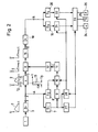
Die Fig.,2 zeigt das Blockschaltbild eines Diskriminators zum Durchführen des Verfahrens.2 shows the block diagram of a discriminator for performing the method.
In einem Detektor 1 nach Patentanmeldung P 30 o3 9o9.9-33 zum gleichzeitigen Messen von α - und/oder β -Teilchen werden Detektorimpulse 2 erzeugt, die zum Ausgleichen von durch den Aufbau des Detektors bedingten Signalabschwächungen mit einem in den Detektor 1 integrierten ersten Verstärker 3 verstärkt werden, der eine Ausgangsimpendanz von 50 Ohm aufweist. Das hat den Vorteil, daß der Detektor mit einem 50 Ohm Koaxkabel über eine den Detektorimpuls 2 um eine vorbestimmte Zeit t2 verzögernde Verzögerungsleitung 4 auf einen den Anstieg der Vorderflanke 5 des Detektorimpulses 2 nach einer vorbestimmten für die Zeitdiskriminierung eingestellten Zeit t1 unterbrechenden elektronischen Schalters 6 geschaltet werden kann.In a
Der Ausgang A des Detektors 1 ist auf einen ersten Komparator 7 mit einer vorbestimmten ersten Schwelle S1 und auf einen zweiten Komparator 8 mit einer vorbestimmten zweiten Schwelle S2 > S1 geschaltet.The output A of the
Der nichtinvertierende Ausgang des ersten Komparators 7 ist über ein digitales Verzögerungsglied 9, der invertierende Ausgang des zweiten Komparators 8 direkt auf eine Startschaltung lo geschaltet, welche ausschließlich bei die zweite Schwelle S2 überschreitenden Amplituden A des Detektorimpulses 2 die Startschaltung lo triggert.The non-inverting output of the
Der Ausgang der Startschaltung lo ist auf eine Pegelanpassung 11 geschaltet, die eine Änderung des Eingangssignales von "O" auf "1" in eine Spannungsänderung von O auf -5 Volt umsetzt.The output of the start circuit lo is switched to a
Ein der Pegelanpassung 11 nachgeschalteter Torzeitimpulsgenerator 12 erzeugt Torzeitimpulse 13 vorbestimmter, konstanter im Nanosekundenbereich liegender Impulsbreite t3.A gate
Der Ausgang des Torzeitimpulsgenerators 12 ist auf den Steuereingang des durch den Torzeitimpuls 13 während der Zeit t1 aufsteuerbaren elektronischen Schalters 6 geschaltet.The output of the gate
Die Zeitverzögerung t2 des Detektorimpulses ist bestimmt durch die Zeitverzögerungen der für die Signalverarbeitung erforderlichen Bauelemente und ist eingestellt durch die Verzögerungsleitung 4.The time delay t 2 of the detector pulse is determined by the time delays of the components required for signal processing and is set by the
Die Vorderflanke 14 des Torzeitimpulses 13 liegt unmittelbar vor dem Ablauf der Verzögerungszeit t2. Der elektronische Schalter 6 wird durch die Rückflanke 15 des Torzeitimpulses 13 gesperrt. Die Rückflanke 15 bestimmt also auch das Ende der für die Zeitdiskriminierung vorgesehene Zeit t und stoppt den Anstieg der Vorderflanke 5 des Detektorimpulses 2 bei einem Amplitudenwert Aα, Aβ.The leading
Dem elektronischen Schalter 6 ist ein Impulsformer 16 nachgeschaltet, der die den Amplituden Aα, Aβ entsprechenden Signalspannungen des zeitdiskriminierten Detektorimpulses 2 in eine elektrische Ladung eines Kondensators umsetzt und den peakförmigen Höchstwert 17 der durch die Zeitdiskriminierung gewonnenen Amplituden Aα, Aβ zeitlich dehnt.The
Der Ausgang des Impulsformers 16 ist über einen zweiten Verstärker 18 auf die Eingänge eines dritten Komparators 19 mit einer vorbestimmten dritten Schwelle S3 > S2 und eines vierten Komparators 2o mit einer vorbestimmten vierten Schwelle S4 > S3 geschaltet.The output of the
Der invertierende Ausgang des dritten Komparators 19 ist auf einen vierten Speicher 21, der invertierende. Ausgang des vierten Komparators 2o ist auf einen fünften Speicher 22 geschaltet.The inverting output of the
Die Ausgänge des vierten Speichers 21 und des fünften Speichers 22 sind auf eine die zeit und amplitudendiskriminierten Detektorimpuls in α-Signale, β-Signale und α- oder β-Signale sortierende Auswertelogik 23 nachJeschaltet.The outputs of the
Der Auswertelogik 23 ist ein erster Zähler 24 für α -Signale, ein zweiter Zähler 25 für β -Signale und ein dritter Zähler 26 für α- oder β -Signale nachgeschaltet.The
Dem invertierenden Ausgang des ersten Komparators 7 ist ein Zeitglied 27 nachgeschaltet, dessen Ausgang mit der Auswertelogik 23 verbunden ist.The inverting output of the
Am Ende der Meßzeit erzeugt das Zeitglied einen Leseimpuls zum übertragen des Inhaltes des vierten Speichers 21 oder des fünften Speichers 22 über die Auswertelogik 23 in einen der Zähler 24, 25, 26. Dem invertierenden Ausgang des ersten Komparators 7 ist eine Resetlogik 28 nachgeschaltet, deren zweiter Eingang mit dem Ausgang des Zeitgliedes 27 verbunden ist und deren Ausgang auf die Reseteingänge der Speicher,der Resetlogik 28, der Startschaltung lo und des vierten und fünften Speichers 21, 22 geschaltet ist.At the end of the measuring time, the timer generates a read pulse for transferring the contents of the
Jeder der Speicher besteht aus einer bistabilen Kippstufe.Each of the stores consists of a bistable flip-flop.
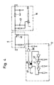
Fig. 3 zeigt das Schaltbild der Komparatoren, der Speicher, der Startschaltung lo, der Auswertelogik 23 und der Resetlogik 28.FIG. 3 shows the circuit diagram of the comparators, the memories, the
Die Startschaltung lo erzeugt ausschließlich bei die zweite Schwelle S2 überschreitenden Signalamplituden Ay, Aβ an ihrem Ausgang 3o ein die Pegelanpassung 11 triggerndes Signal.The start circuit lo generates only at the second threshold S 2 exceeding signal amplitudes Ay, A β at its output 3o a signal triggering the
Die Startschaltung lo besteht aus einer zweiten bistabilen Kippstufe 31, einer dritten bistabilen Kippstufe 32, einem zweiten NAND-Gatter 33 und einem dritten NAND-Gatter 34.The
Dem zweiten NAND-Gatter 33, dessen erster Eingang auf den Ausgang des digitalen Verzögerungsgliedes 9 und dessen zweiter Eingang auf den invertierenden Ausgang des zweiten Komparators 8 geschaltet ist, ist die zweite bistabile Kippstufe 31 nachgeschaltet.The second
Der nichtinvertierende Ausgang 35 der zweiten Kippstufe 31 ist auf den ersten Eingang des dritten NAND-Gatters 34 geschaltet, dessen zweiter Eingang mit dem nichtinvertierenden Ausgang des zweiten Komparators 8 verbunden ist.The non-inverting output 35 of the second flip-
Dem Ausgang des dritten NAND-Gatters 34 ist die dritte bistabile Kippstufe 32 nachgeschaltet, deren invertierender Ausgang 3o auf die Pegelanpassung 11 geschaltet ist.The output of the
Die Pegelanpassung 11 besteht im wesentlichen aus einem pnp-Transistor 36, dessen Basis auf den Ausgang 3o der Startschaltung lo, dessen Emitter auf.eine positive Spannung von 5 Volt und dessen Kollektor auf eine nega-tive Spannung von 5 Volt geschaltet ist.The
Der Ausgang der Pegelanpassung 11 ist über den Punkt C der Schaltung mit dem Eingang einer sechsten bistabilen Kippstufe 37 des in Fig. 4 dargestellten Torzeitimpulsgenerators 12 verbunden.The output of the
Der invertierende Ausgang 38 der Kippstufe 37 ist über eine Treiberstufe 39 auf die Steuerelektrode des als Feldeffekttransistor 4o ausgebildeten elektronischen Schalters 6 geschaltet.The inverting
Der nichtinvertierende Ausgang 41 der sechsten bistabilen Kippstufe 37 ist über ein die öffnungszeit t3 des FET 4o bestimmendes Verzögerungsglied 42 auf deren Reseteingang zurückgeführt.The non-inverting output 41 of the sixth
Die fallende Flanke des von der Pegelanpassung 11 erzeugten Steuersignales triggert die sechste bistabile Kippstufe 37, deren-invertierender Ausgang 38 von -5 Volt auf O Volt umschaltet und dadurch die Vorderflanke 14 des in Fig. 1 gezeichneten Torzeitimpulses 13 erzeugt.The falling edge of the control signal generated by the
Gleichzeitig geht der nichtinvertierende Ausgang 41 von O auf -5 Volt. Dieses Signal wird durch das Verzögerungsglied 42 um die Zeit t3 verzögert auf den Reseteingang zurückgeführt und erzeugt die Rückflanke 15 des Torzeitimpulses 13, der die öffnungszeit t3 des elektronischen Schalters 6 bestimmt.At the same time, the non-inverting output 41 goes from 0 to -5 volts. This signal is fed back to the reset input by the
Von dem am Punkt D der Schaltung ankommenden Detektorimpuls 2 gelangt über den elektronischen Schalter 6 ein durch dessen öffnungszeit t3 (Zeitdiskriminierung) begrenzten Teil der Vorderflanke 5 zum Impulsformer 16, dessen Kondensator 43 während der Zeit t3 aufgeladen wird und sich bis zum Beginn des nächsten Meßzyklus anschließend entlädt. Ein nachgeschaltetes Integrierglied 44 bewirkt eine zeitliche Dehnung des peakförmigen Höchstwertes 17 der durch die Zeitdiskriminierung gewonnenen Impulsamplituden AO(, Aβ, die über den Punkt E der Schaltung den zweiten Verstärker 18 und den Punkt B der Schaltung auf den die Amplitudendiskriminierung bewirkenden Teil der Schaltungsanordnung übertragen werden.From the
Der nichtinvertierende Ausgang 45 des als bistabile Kippstufe ausgebildeten vierten Speichers 21 ist auf einen ersten Eingang eines ersten UND-Gatters 46 der invertierende Ausgang 47 ist auf einen ersten Eingang eines zweiten UND-Gatters 48 geschaltet, dessen zweiter Eingang auf den nichtinvertierenden Ausgang 49 des fünften Speichers 22 geschaltet ist.The
Der invertierende Ausgang 5o des fünften Speichers 22 ist auf einen ersten Eingang eines dritten UND-Gatters 51 geschaltet.The inverting
Der Ausgang des zweiten UND-Gatters 48 ist auf einen ersten Eingang eines vierten UND-Gatters 52 geschaltet. Der zweite Eingang des ersten UND-Gatters 46, der zweite Eingang des dritten UND-Gatters 51 und der zweite Eingang des vierten UND-Gatters 52 sind auf den Ausgang des Zeitgliedes 27 geschaltet.The output of the second AND
Der Ausgang des ersten UND-Gatters 46 ist auf einen die B-Ereignisse zählenden zweiten Zähler 25, der Ausgang des dritten UND-Gatters 51 ist auf einen die α-Ereignisse zählenden ersten Zähler 24 und der Ausgang des vierten UND-Gatters 52 ist auf einen die weder dem α - noch dem ß-Zähler 24, 25 eindeutig zuzuordnenden, α- und B-Ereignisse zählenden dritten Zähler 26 geschaltet. Das erste bis vierte UND-Gatter 46, 48, 51, 52 bildet die Auswertelogik 23.The output of the first AND
Dem invertierenden Ausgang des ersten Komparators 7 ist eine erste monostabile Kippstufe 53 und dieser eine zweite monostabile Kippstufe 54 nachgeschaltet; die beiden Kippstufen bilden das Zeitglied 27. Der Ausgang des Zeitgliedes 27 ist auf den Eingang einer ersten bistabilen Kippstufe 55 geschaltet, deren invertierender Ausgang 56 mit dem ersten Eingang eines ersten NAND-Gatters 57 verbunden ist. Der zweite Eingang des ersten NAND-Gatters 57 ist auf den invertierenden Ausgang des ersten Komparators 7 geschaltet. Der Ausgang des ersten NAND-Gatters 57 ist auf die Rückstelleingänge der ersten bis fünften bistabilen Kippstufen 55, 31, 32, 21, 22 geschaltet. Die erste bistabile Kippstufe 55 und das erste NAND-Gatter 57 bilden die Resetlogik 28.The inverting output of the
Abhängig von der Signalamplitude existieren unterschiedliche Möglichkeiten der Signalverarbeitung,Depending on the signal amplitude, there are different possibilities for signal processing,
S1 < A < S2 Wenn die Amplitude A des Detektorsignales 2 die erste Schwelle S1 überschreitet, jedoch die zweite Schwelle S2 nicht erreicht, wird der nichtinvertierende Ausgang des ersten Komparators 7 und damit der erste Eingang des zweiten NAND-Gatters 33 von "O" auf "1" gesetzt.S 1 <A <S 2 If the amplitude A of the
Der zweite Eingang des zweiten NAND-Gatters 33, der mit dem invertierenden Ausgang des zweiten Komparators 8 verbunden ist, bleibt auf '1', so daß der Ausgang des zweiten NAND-Gatters 33 und damit der Eingang der zweiten bistabilen Kippstufe 31 und deren nichtinvertierender Ausgang von '1' auf '0' wechselt.The second input of the second NAND gate 33, which is connected to the inverting output of the
Der erste Eingang des dritten NAND-Gatters 34 geht also auf '0', der zweite Eingang bleibt auf 'O' und der Ausgang bleibt auf '1',so daß der invertierende Ausgang des dritten Speichers 32 auf 'O' bleibt und die Startschaltung lo einen Meßvorgang mit Zeit-und Amplitudendiskrimination nicht einleitet.The first input of the
Der invertierende Ausgang des ersten Komparators 7 wechselt gleichzeitig von '1' auf '0'. Die fallende Flanke stößt die erste monostabile Kippstufe 53 und diese zeitverzögert eine zweite monostabile Kippstufe 54 des Zeitgliedes 27 an, dessen Ausgang auf den ersten Eingang des ersten UND-Gatters 46 der Auswertelogik 23 geschaltet ist. Der zweite Eingang des ersten UND-Gatters 46 steht auf '1', so daß durch das '1'-Signal des Zeitgliedes 27 ausschließlich der dem ersten UND-Gatter 38 nachgeschaltete zweite Zähler 25 für ß-Signale einen Zählimpuls erhält.The inverting output of the
A > S2 Wenn die Amplitude A des Detektorsignales 2 die erste Schwelle S1 und die zweite Schwelle S2 überschreitet, wechselt der nichtinvertierende Ausgang des zweiten Komparators 8 und damit auch der zweite Eingang des dritten NAND-Gatters 34 von "O" auf "1". Dessen erster Eingang ist auf "l", so daß der Ausgang von "1" auf "O" geht. Die fallende Flanke setzt den dritten Speicher 32 und der Ausgang 3o der Startschaltung lo wechselt von 'O' auf '1'.A> S 2 If the amplitude A of the detector signal 2 exceeds the first threshold S 1 and the second threshold S 2 , the non-inverting output of the
Die Pegelanpassung 11 setzt den Triggerimpuls der Startschaltung lo in eine Spannungsänderung von O Volt auf -5 Volt um. Diese fallende Flanke setzt die sechste bistabile Kippstufe 37, die mit einer Betriebsspannung von O und -5 Volt arbeitet. Der invertierende Ausgang 38 wechselt von -5 Volt auf O Volt und erzeugt die den Schalter 6 öffnende Vorderflanke 14 des Torzeitimpulses 13 (s.Fig. l). Der nichtinvertierende Ausgang 41 stellt nach einer durch das Verzögerungsglied 42 bestimmbaren Zeit t3 von ca. 3o ns die Kippstufe zurück. Dabei wird die den Schalter 6 schließende Rückflanke 15 des Torzeitimpulses 13 erzeugt. Das zeitdiskriminierte Detektorsignal wird nun zur Bestimmung der Amplitude amplitudendiskriminiert.The
Dabei sind folgende Fälle möglich:
S2 < A < S3 eindeutiges β-Signal Die Amplitude A des Detektorimpulses 2 ist größer als die Schwelle S1 und S2, so daß eine Zeitdiskriminierung ausgelöst wird (siehe A>S2). Da jedoch die Schwelle S3 nicht erreicht wird, bleiben die Ausgänge 45, 47 und 49, 5o des vierten und des fünften Speichers 21, 22 unverändert.Ausschließlich der dem nichtinvertierenden Ausgang des vierten Speichers 21 nachgeschaltete erste Eingang des ersten UND-Gatters 46 der Auswertelogik 23 steht auf '1', so daß das '1'-Signal des Zeitgliedes 27 ausschließlich den Ausgang des ersten UND-Gatters 46 auf '1' setzt und der zweite Zähler 25 ein β-Signal zählt.
S3< A < S4 α - oder β -Signal Wie unter A > S2 erläutert wird eine Zeitdiskriminierung ausgelöst. Der invertierende Ausgang des dritten Komparators 19 und der nichtinvertierende Ausgang 45 des vierten Speichers 21 geht von '1' auf '0', der invertierende Ausganqs 47 des Speichers 21 wechselt von '0' auf '1'. Am fünften Speicher 22 bleibt der nichtinvertierende Ausgang 49 auf 1 und der invertierende Ausgang 51 auf O. Der erste und der zweite Eingang des zweiten UND-Gatters 48 und damit dessen Ausgang sind auf '1'. Das vierte UND-Gatter 52 führt damit an seinem ersten und zweiten Eingang und an seinem Ausgang eine '1', so daß der dritte Zähler 26 einen Zählimpuls erhält. Je weniger Impulse der Zähler 26 zählt, umso besser ist die Meßeinrichtung.
A > S4 eindeutiges α-Signal Der invertierende Ausgang des vierten Komparators 20 geht von '1' auf '0', der invertierende Ausgang 50 des fünften Speichers 22 wechselt von '0' auf '1'. Da die Schwelle S1 überschritten ist, werden über den Ausgang des Zeitgliedes 27 den ersten Eingängen des ersten, dritten und vierten UND-Gatters 46, 51, 52 auf '1' gestellt. Damit geht der Ausgang des dritten UND-Gatters auf '1' und der erste Zähler 24 zählt einen α-Impuls. Der zweite und der dritte Zähler 25, 26 erhalten keinen Zählimpuls, da die zweiten Eingänge der dem Zähler vorgeschalteten ersten und vierten UND-Gatter 46, 52 auf '0' stehen.The following cases are possible:
S 2 <A <S 3 β unambiguous signal, the amplitude A of the
S 3 <A <S 4 α or β signal As explained under A> S 2 , time discrimination is triggered. The inverting output of the
A> S 4 unique α signal The inverting output of the
Der positive-Impuls der zweiten monostabilen Kippstufe 54 wird also als Lesesignal für den vierten und fünften Speicher 21; 22 verwendet. Während der Zeit, in der der Ausgang der ersten monostabilen Kippstufe 53 auf '1' liegt, läuft die Zeitdiskriminierung. Die Rückflanke des Impulses am Ausgang der zweiten monostabilen Kippstufe 54 beendet den Lesevorgang des vierten und fünften Speichers 21, 22 und setzt gleichzeitig den invertierten Ausgang 56 der ersten bistabilen Kippstufe 55 und den ersten Eingang des ersten NAND-Gatters 57 auf '1'. Liegt dessen anderer, mit dem invertierenden Ausgang des ersten Komparators 7 verbundener Eingang ebenfalls auf '1', so geht der Ausgang des ersten NAND-Gatters 57 auf '0'. Dadurch werden der erste bis fünfte Speicher 55, 31, 32, 21, 22 in eine vorbestimmte Ausgangsstellung zurückgesetzt und für eine neue Messung vorbereitet.The positive pulse of the second
Die Verknüpfung des Ausganges 56 des ersten Speichers 55 mit dem invertierenden Ausgang des ersten Komparators 7 stellt sicher, daß der Resetimpuls nur dann auf die Speicher gegeben wird, wenn sicher ist, daß die Schwelle S1 des ersten Komparators 7 nicht überschritten wurde, also sich kein Detektorsignal 2 auf der Leitung befindet.The combination of the
Die Impulslänge eines α - oder ß-Impules beträgt ca. 150 ns, die für eine Messung erforderliche Zeit ist etwa 1,2 µs. Wegen der statistischen Verteilung der Impulse können während einer Messung ein oder mehrere weitere Impulse auftreten. Sobald ein Meßvorgang durch Setzen des dritten Spreichers 32 eingeleitet ist, werden deshalb weitere α- oder ß-Impulse durch die Schaltung unterdrückt, bis nach dem Resetimpuls deren Meßbereitschaft wieder hergestellt ist.The pulse length of an α or β pulse is approx. 150 ns, the time required for a measurement is approx. 1.2 µs. Because of the statistical distribution of the pulses, one or more additional pulses can occur during a measurement. As soon as a measuring process is initiated by setting the
Voraussetzung für eine exakte Messung ist, daß der Rücksetzimpuls zeitlich zwischen zwei Meßsignale fällt, so daß die Meßeinrichtung beim Eingang eines Detektorsignales 2 betriebsbereit ist.Precondition for an exact measurement is that the reset pulse falls in time between two measurement signals, so that the measuring device is ready for operation when a
Durch die Verknüpfungen der Schaltungsanordnung ist sichergestellt, daß die Zeitdiskriminierung immer mit dem Anstieg der Vorderflanke des Detektorsignales 2 beginnt.The links in the circuit arrangement ensure that the time discrimination always begins with the rising front edge of the
-
Fig. 1
- a Steigung der Vorderflanke eines von a-Teilchen erzeugten Detektorimpulses in der Zeit t 2
- ß entsprechend a- für ß-Teilchen
- t1 für die Zeitdiskriminierung eingestellte Zeit in ns
- Aα,Aβ Impulsamplitude
- ΔUα Amplitude des a-Impulses zur Zeit t1
- ΔUβ Amplitude des β-Impulses zur Zeit t1
- t2 Verzögerung des Detektorimpulses
- t3 Breite des Torzeitimpulses, Öffnungszeit von 6
- a slope of the leading edge of a detector pulse generated by a particles in time t 2
- ß corresponding to a- for ß particles
- t1 time set for the time discrimination in ns
- A α , A β pulse amplitude
- ΔU α amplitude of the a pulse at time t 1
- ΔU β amplitude of the β pulse at time t 1
- t2 delay of the detector pulse
- t 3 Width of the gate pulse, opening time of 6
-
Fig. 2
- 1 Detektor
- 2 Detektorimpulse
- 3 1. Verstärker
- 4 Verzögerungsleitung
- 5 Vorderflanke von 2
- 6 elektronischer Schalter
- 7 1. Komparator
- S1 1. Schwelle an 7
- 8 2. Komparator
- S2: Schwelle an 8
- 9 digitales Verzögerungsglied
- 10 Startschaltung
- 11 Pegelanpassung
- 12 Torzeitimpulsgenerator 13 Torzeitimpuls
- 14 Vorderflanke von 13
- 15 Rückflanke von 13
- 16 Impulsformer
- 17 Höchstwert von ΔUα, ΔUβ
- 18 2. Verstärker
- 19 3. Komparator
- S3 3. Schwelle von 19
- 20 4. Komparator
- S4 4. Schwelle von 20
- 21 4. Speicher (bistab. Kippstufe)
- 22 5. Speicher (bistab. Kippstufe)
- 23 Auswertelogik
- 24 1. Zähler
- 25 2. Zähler
- 26 3. Zähler
- 27 Zeitglied
- 28 Resetlogik
- 1 detector
- 2 detector pulses
- 3 1. Amplifier
- 4 delay line
- 5 leading edge of 2
- 6 electronic switches
- 7 1. Comparator
-
S 1 1. Threshold at 7 - 8 2. Comparator
- S 2 : threshold at 8
- 9 digital delay element
- 10 start circuit
- 11 level adjustment
- 12 gate
time pulse generator 13 gate time pulse - 14 leading edge of 13
- 15 trailing edge of 13
- 16 pulse shapers
- 17 Maximum value of ΔU α , ΔU β
- 18 2. Amplifier
- 19 3. Comparator
- S 3 3rd threshold of 19
- 20 4. Comparator
- S 4 4th threshold of 20
- 21 4th memory (bistable flip-flop)
- 22 5th memory (bistable flip-flop)
- 23 Evaluation logic
- 24 1st counter
- 25 2nd counter
- 26 3rd counter
- 27 timer
- 28 Reset logic
-
Fig. 3
- 30 Ausgang von 10
- 31 2. bistabile Kippstufe
- 32. 3. bistabile Kippstufe
- 33 2. NAND-Gatter
- 34 3. NAND-Gatter
- 35 nichtinvertierender Ausgang von 31
- 36 pnp-Transistor von 11
- 37 6. bistabile Kippstufe
- 38 invert. Ausgang von 37
- 39 Treiberstufe
- 40 FET von 6
- 41 nichtinvert. Ausgang von 37
- 42 Verzögerungsglied von 12
- 43 Kondensator in 16
- 44 Integrierglied
- 45 nichtinvert. Ausgang von 21
- 46 1.UND-Gatter von 23
- 47 invertierender Ausgang von 21
- 48 2. UND-Gatter von 23
- 49 nichtinvert. Ausgang von 22
- 50 invert. Ausgang von 22
- 51 3. UND-Gatter von 23
- 52 4. UND-Gatter von 23
- 53 1. monostabile Kippstufe von 27
- 54 2. monostabile Kippstufe von 27
- 55 1. bistabile Kippstufe von 28
- 56 invertierender Ausgang von 55
- 57 1. NAND-Gatter von 55
- 30 exit of 10
- 31 2nd bistable flip-flop
- 32. 3rd bistable flip-flop
- 33 2. NAND gate
- 34 3. NAND gate
- 35 non-inverting output from 31
- 36 pnp transistor from 11
- 37 6. bistable flip-flop
- 38 invert. Exit from 37
- 39 driver stage
- 40 FET of 6
- 41 non-inverted. Exit from 37
- 42 delay element of 12
- 43 capacitor in 16
- 44 integrator
- 45 non-inverted. Exit from 21
- 46 1st AND gate of 23
- 47 inverting output from 21
- 48 2nd AND gate of 23
- 49 non-inverted. Exit from 22
- 50 invert. Exit from 22
- 51 3rd AND gate of 23
- 52 4th AND gate of 23
- 53 1st monostable multivibrator from 27
- 54 2nd monostable multivibrator from 27
- 55 1st bistable flip-flop of 28
- 56 inverting output from 55
- 57 1. NAND gate of 55
Claims (9)
gekennzeichnet durch folgende Merkmale,
characterized by the following features,
gekennzeichnet durch folgende Merkmale,
characterized by the following features,
Priority Applications (4)
| Application Number | Priority Date | Filing Date | Title |
|---|---|---|---|
| DE8181103119T DE3173230D1 (en) | 1981-04-25 | 1981-04-25 | Method and circuit for the discrimination of alpha and beta particles |
| EP81103119A EP0063624B1 (en) | 1981-04-25 | 1981-04-25 | Method and circuit for the discrimination of alpha and beta particles |
| US06/283,189 US4454587A (en) | 1981-04-25 | 1981-07-14 | Method and circuit arrangement for discriminating between pulses generated by alpha and/or beta radiators |
| JP57037872A JPS57179774A (en) | 1981-04-25 | 1982-03-10 | Method and device for selecting pulse by alpha particle and pulse by beta particle |
Applications Claiming Priority (1)
| Application Number | Priority Date | Filing Date | Title |
|---|---|---|---|
| EP81103119A EP0063624B1 (en) | 1981-04-25 | 1981-04-25 | Method and circuit for the discrimination of alpha and beta particles |
Publications (2)
| Publication Number | Publication Date |
|---|---|
| EP0063624A1 true EP0063624A1 (en) | 1982-11-03 |
| EP0063624B1 EP0063624B1 (en) | 1985-12-18 |
Family
ID=8187678
Family Applications (1)
| Application Number | Title | Priority Date | Filing Date |
|---|---|---|---|
| EP81103119A Expired EP0063624B1 (en) | 1981-04-25 | 1981-04-25 | Method and circuit for the discrimination of alpha and beta particles |
Country Status (4)
| Country | Link |
|---|---|
| US (1) | US4454587A (en) |
| EP (1) | EP0063624B1 (en) |
| JP (1) | JPS57179774A (en) |
| DE (1) | DE3173230D1 (en) |
Cited By (1)
| Publication number | Priority date | Publication date | Assignee | Title |
|---|---|---|---|---|
| DE3125978A1 (en) * | 1981-07-01 | 1983-01-20 | Laboratorium Prof. Dr. Rudolf Berthold, 7547 Wildbad | METHOD AND DEVICE FOR THE SPECIFIC DETECTION OF (ALPHA) RAYS AND / OR (BETA) - AND (GAMMA) RAYS IN PROPORTIONAL COUNTER TUBES WITH THE PRESENCE OF EACH OTHER RADIATION TYPE AND APPLICATION |
Families Citing this family (10)
| Publication number | Priority date | Publication date | Assignee | Title |
|---|---|---|---|---|
| US5124936A (en) * | 1990-10-31 | 1992-06-23 | Science Applications International Corporation | Method and apparatus for measuring airborne uranium and transuranium elements |
| US5347129A (en) * | 1993-04-14 | 1994-09-13 | University Of Missouri-Columbia | System for determining the type of nuclear radiation from detector output pulse shape |
| US5475312A (en) * | 1994-06-07 | 1995-12-12 | Iris Power Engineering Inc. | Method and device for distinguishing between partial discharge and electrical noise |
| US6771712B2 (en) * | 2001-07-27 | 2004-08-03 | The Pulsar Network, Inc. | System for extracting a clock signal and a digital data signal from a modulated carrier signal in a receiver |
| CA2412488C (en) | 2001-12-11 | 2009-09-08 | Crompton Gmbh | Process for preparing partial hydrolysates of organometallic compounds or transition metal catalysts immobilized on inert support materials |
| DE102004009104A1 (en) * | 2004-02-25 | 2005-09-22 | Berthold Technologies Gmbh & Co. Kg | Method and device for detecting ionizing radiation |
| US10031060B2 (en) | 2016-07-13 | 2018-07-24 | Mauro & Associates, Llc | Continuous, real time monitor for airborne depleted uranium particles in the respiratory range and corresponding method of use |
| CN109557573B (en) * | 2018-11-29 | 2022-07-15 | 中广核久源(成都)科技有限公司 | Digital alpha/beta ray discrimination method |
| CN113075720B (en) * | 2021-03-24 | 2024-05-31 | 福州智元仪器设备有限公司 | Alpha and beta ray discrimination system and method based on combined timer |
| CN115079244B (en) * | 2022-06-30 | 2023-05-30 | 成都理工大学工程技术学院 | Digital n/gamma screening method based on gradient of falling edge amplitude percentage point |
Citations (1)
| Publication number | Priority date | Publication date | Assignee | Title |
|---|---|---|---|---|
| US4262203A (en) * | 1979-02-02 | 1981-04-14 | Overhoff Mario W | Alpha particle monitor |
Family Cites Families (7)
| Publication number | Priority date | Publication date | Assignee | Title |
|---|---|---|---|---|
| US3578960A (en) * | 1966-04-06 | 1971-05-18 | Beckman Instruments Inc | Radiation detection system with automatic sample counting rate determination |
| US3486025A (en) * | 1966-09-15 | 1969-12-23 | Lfe Corp | Apparatus for analyzing the energy distribution of a radioisotope in the presence of interfering radiation |
| US3638000A (en) * | 1966-10-07 | 1972-01-25 | Comitato Nazionale Per 1 En Nu | Method and apparatus for continuously determining the quantities of the qualitatively known radioactive nuclides contained in a physical system |
| US3717753A (en) * | 1969-10-01 | 1973-02-20 | Intertechnique Sa | Liquid scintillation spectrometer with automatic setting of channel limits |
| NL7110516A (en) * | 1971-07-30 | 1973-02-01 | ||
| US3906377A (en) * | 1974-07-23 | 1975-09-16 | Us Navy | Pulse centroid detector |
| US4228512A (en) * | 1978-05-03 | 1980-10-14 | The Dow Chemical Company | Nuclear pulse counting apparatus and technique |
-
1981
- 1981-04-25 DE DE8181103119T patent/DE3173230D1/en not_active Expired
- 1981-04-25 EP EP81103119A patent/EP0063624B1/en not_active Expired
- 1981-07-14 US US06/283,189 patent/US4454587A/en not_active Expired - Fee Related
-
1982
- 1982-03-10 JP JP57037872A patent/JPS57179774A/en active Granted
Patent Citations (1)
| Publication number | Priority date | Publication date | Assignee | Title |
|---|---|---|---|---|
| US4262203A (en) * | 1979-02-02 | 1981-04-14 | Overhoff Mario W | Alpha particle monitor |
Non-Patent Citations (1)
| Title |
|---|
| Instruments and Experimental Techniques, Band 18, Nr. 6, Teil 1, November/Dezember 1975, seiten 1764-1767 New York, U.S.A. E.N. KUZIN et al.: "Devide for Identifying Recoil Protons According to the Shape of the Pulses in a Proportional Counter" * Abbildung 1a * * |
Cited By (1)
| Publication number | Priority date | Publication date | Assignee | Title |
|---|---|---|---|---|
| DE3125978A1 (en) * | 1981-07-01 | 1983-01-20 | Laboratorium Prof. Dr. Rudolf Berthold, 7547 Wildbad | METHOD AND DEVICE FOR THE SPECIFIC DETECTION OF (ALPHA) RAYS AND / OR (BETA) - AND (GAMMA) RAYS IN PROPORTIONAL COUNTER TUBES WITH THE PRESENCE OF EACH OTHER RADIATION TYPE AND APPLICATION |
Also Published As
| Publication number | Publication date |
|---|---|
| DE3173230D1 (en) | 1986-01-30 |
| US4454587A (en) | 1984-06-12 |
| JPS57179774A (en) | 1982-11-05 |
| JPH0315714B2 (en) | 1991-03-01 |
| EP0063624B1 (en) | 1985-12-18 |
Similar Documents
| Publication | Publication Date | Title |
|---|---|---|
| EP0063624B1 (en) | Method and circuit for the discrimination of alpha and beta particles | |
| DE3039840C2 (en) | Time interval measuring device | |
| DE1905176C3 (en) | Process for analog-digital conversion with improved differential linearity of the conversion and arrangement for carrying out this process | |
| DE3419117A1 (en) | OPTOELECTRICAL DISTANCE MEASURING DEVICE WITH A TIME DISCRIMINATOR FOR ACCURATE DETERMINATION OF THE TIMING OF ELECTRICAL IMPULSES | |
| DE1288632B (en) | Analog / digital converter with an integrating amplifier | |
| DE2847619C2 (en) | ||
| DE2127283A1 (en) | Method and device for measuring the frequency of electrical signals | |
| DE2728150C2 (en) | Analog / digital converter | |
| DE3706089A1 (en) | TIME MEASURING SYSTEM WITH A LARGE DYNAMIC RANGE | |
| DE2503538A1 (en) | DEVICE FOR GENERATING A TIME REFERENCE SIGNAL FROM A PULSE OF ELECTRIC SIGNAL VIBRATIONS | |
| DE2235366B2 (en) | CIRCUIT FOR SIGNAL SUPPRESSION | |
| DE2653501B2 (en) | Frequency comparison circuit | |
| CH643972A5 (en) | LOGARITHMIC ANALOG-DIGITAL CONVERTER. | |
| DE2150174A1 (en) | Device for indicating the end of a chromatographic signal | |
| DE3783893T2 (en) | FREQUENCY VOLTAGE CONVERTER. | |
| EP0942564A2 (en) | Method for detecting a pulsed signal | |
| DE2352772A1 (en) | I.C. engine ignition angular impulse transmitter - has pre-, time and division meters with balancing stages | |
| DE2725618C3 (en) | Device for measuring the integral of a time-dependent physical quantity | |
| DE3322471A1 (en) | Measuring arrangement for detecting current or voltage values | |
| DE4222643A1 (en) | Device for measuring pulse transit times | |
| DE3322483A1 (en) | Measuring arrangement for detecting current or voltage values | |
| EP0141122B1 (en) | Circuit arrangement for measuring short time intervals | |
| DE3608440A1 (en) | PULSE LENGTH DISCRIMINATOR | |
| DE2803105C2 (en) | ||
| DE2755492C2 (en) |
Legal Events
| Date | Code | Title | Description |
|---|---|---|---|
| PUAI | Public reference made under article 153(3) epc to a published international application that has entered the european phase |
Free format text: ORIGINAL CODE: 0009012 |
|
| AK | Designated contracting states |
Designated state(s): BE CH DE FR GB NL |
|
| 17P | Request for examination filed |
Effective date: 19830321 |
|
| GRAA | (expected) grant |
Free format text: ORIGINAL CODE: 0009210 |
|
| AK | Designated contracting states |
Designated state(s): BE CH DE FR GB LI NL |
|
| REF | Corresponds to: |
Ref document number: 3173230 Country of ref document: DE Date of ref document: 19860130 |
|
| ET | Fr: translation filed | ||
| PLBE | No opposition filed within time limit |
Free format text: ORIGINAL CODE: 0009261 |
|
| STAA | Information on the status of an ep patent application or granted ep patent |
Free format text: STATUS: NO OPPOSITION FILED WITHIN TIME LIMIT |
|
| 26N | No opposition filed | ||
| PGFP | Annual fee paid to national office [announced via postgrant information from national office to epo] |
Ref country code: NL Payment date: 19870430 Year of fee payment: 7 |
|
| PG25 | Lapsed in a contracting state [announced via postgrant information from national office to epo] |
Ref country code: GB Effective date: 19890425 |
|
| PG25 | Lapsed in a contracting state [announced via postgrant information from national office to epo] |
Ref country code: LI Effective date: 19890430 Ref country code: CH Effective date: 19890430 Ref country code: BE Effective date: 19890430 |
|
| BERE | Be: lapsed |
Owner name: KERNFORSCHUNGSZENTRUM KARLSRUHE G.M.B.H. Effective date: 19890430 |
|
| PG25 | Lapsed in a contracting state [announced via postgrant information from national office to epo] |
Ref country code: NL Effective date: 19891101 |
|
| NLV4 | Nl: lapsed or anulled due to non-payment of the annual fee | ||
| GBPC | Gb: european patent ceased through non-payment of renewal fee | ||
| PG25 | Lapsed in a contracting state [announced via postgrant information from national office to epo] |
Ref country code: FR Free format text: LAPSE BECAUSE OF NON-PAYMENT OF DUE FEES Effective date: 19891228 |
|
| REG | Reference to a national code |
Ref country code: CH Ref legal event code: PL |
|
| REG | Reference to a national code |
Ref country code: FR Ref legal event code: ST |
|
| PGFP | Annual fee paid to national office [announced via postgrant information from national office to epo] |
Ref country code: DE Payment date: 20000404 Year of fee payment: 20 |