EP0075454B1 - Halbleiteranordnung mit leitender Verbindungsstruktur und Verfahren zum Herstellen derselben - Google Patents
Halbleiteranordnung mit leitender Verbindungsstruktur und Verfahren zum Herstellen derselben Download PDFInfo
- Publication number
- EP0075454B1 EP0075454B1 EP82304904A EP82304904A EP0075454B1 EP 0075454 B1 EP0075454 B1 EP 0075454B1 EP 82304904 A EP82304904 A EP 82304904A EP 82304904 A EP82304904 A EP 82304904A EP 0075454 B1 EP0075454 B1 EP 0075454B1
- Authority
- EP
- European Patent Office
- Prior art keywords
- layer
- polyacetylene
- region
- conductive layers
- impurity doped
- Prior art date
- Legal status (The legal status is an assumption and is not a legal conclusion. Google has not performed a legal analysis and makes no representation as to the accuracy of the status listed.)
- Expired
Links
Images


Classifications
-
- H—ELECTRICITY
- H10—SEMICONDUCTOR DEVICES; ELECTRIC SOLID-STATE DEVICES NOT OTHERWISE PROVIDED FOR
- H10P—GENERIC PROCESSES OR APPARATUS FOR THE MANUFACTURE OR TREATMENT OF DEVICES COVERED BY CLASS H10
- H10P14/00—Formation of materials, e.g. in the shape of layers or pillars
- H10P14/60—Formation of materials, e.g. in the shape of layers or pillars of insulating materials
- H10P14/68—Organic materials, e.g. photoresists
- H10P14/683—Organic materials, e.g. photoresists carbon-based polymeric organic materials, e.g. polyimides, poly cyclobutene or PVC
-
- H—ELECTRICITY
- H10—SEMICONDUCTOR DEVICES; ELECTRIC SOLID-STATE DEVICES NOT OTHERWISE PROVIDED FOR
- H10K—ORGANIC ELECTRIC SOLID-STATE DEVICES
- H10K85/00—Organic materials used in the body or electrodes of devices covered by this subclass
- H10K85/10—Organic polymers or oligomers
- H10K85/141—Organic polymers or oligomers comprising aliphatic or olefinic chains, e.g. poly N-vinylcarbazol, PVC or PTFE
- H10K85/143—Polyacetylene; Derivatives thereof
-
- H—ELECTRICITY
- H10—SEMICONDUCTOR DEVICES; ELECTRIC SOLID-STATE DEVICES NOT OTHERWISE PROVIDED FOR
- H10W—GENERIC PACKAGES, INTERCONNECTIONS, CONNECTORS OR OTHER CONSTRUCTIONAL DETAILS OF DEVICES COVERED BY CLASS H10
- H10W20/00—Interconnections in chips, wafers or substrates
- H10W20/01—Manufacture or treatment
-
- H—ELECTRICITY
- H10—SEMICONDUCTOR DEVICES; ELECTRIC SOLID-STATE DEVICES NOT OTHERWISE PROVIDED FOR
- H10W—GENERIC PACKAGES, INTERCONNECTIONS, CONNECTORS OR OTHER CONSTRUCTIONAL DETAILS OF DEVICES COVERED BY CLASS H10
- H10W20/00—Interconnections in chips, wafers or substrates
- H10W20/40—Interconnections external to wafers or substrates, e.g. back-end-of-line [BEOL] metallisations or vias connecting to gate electrodes
- H10W20/41—Interconnections external to wafers or substrates, e.g. back-end-of-line [BEOL] metallisations or vias connecting to gate electrodes characterised by their conductive parts
- H10W20/44—Conductive materials thereof
- H10W20/4473—Conductive organic materials, e.g. conductive adhesives or conductive inks
Definitions
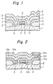
- windows are not opened for via holes and neither of the interconnecting line have steps which in the prior art are formed at the edges of the patterned interconnecting line by being selectively etched.
Landscapes
- Chemical & Material Sciences (AREA)
- Engineering & Computer Science (AREA)
- Materials Engineering (AREA)
- Internal Circuitry In Semiconductor Integrated Circuit Devices (AREA)
Claims (16)
gekennzeichet durch
gekennzeichnet durch
Applications Claiming Priority (4)
| Application Number | Priority Date | Filing Date | Title |
|---|---|---|---|
| JP148094/81 | 1981-09-18 | ||
| JP148092/81 | 1981-09-18 | ||
| JP56148094A JPS5848942A (ja) | 1981-09-18 | 1981-09-18 | 半導体装置とその製造方法 |
| JP56148092A JPS5848940A (ja) | 1981-09-18 | 1981-09-18 | 半導体装置の製造方法 |
Publications (3)
| Publication Number | Publication Date |
|---|---|
| EP0075454A2 EP0075454A2 (de) | 1983-03-30 |
| EP0075454A3 EP0075454A3 (en) | 1984-11-28 |
| EP0075454B1 true EP0075454B1 (de) | 1987-11-25 |
Family
ID=26478428
Family Applications (1)
| Application Number | Title | Priority Date | Filing Date |
|---|---|---|---|
| EP82304904A Expired EP0075454B1 (de) | 1981-09-18 | 1982-09-17 | Halbleiteranordnung mit leitender Verbindungsstruktur und Verfahren zum Herstellen derselben |
Country Status (3)
| Country | Link |
|---|---|
| US (1) | US4761677A (de) |
| EP (1) | EP0075454B1 (de) |
| DE (1) | DE3277759D1 (de) |
Families Citing this family (16)
| Publication number | Priority date | Publication date | Assignee | Title |
|---|---|---|---|---|
| CA1215789A (en) * | 1983-10-19 | 1986-12-23 | Timothy W. Johnson | Conductive patterns in polymeric films |
| JPS6185844A (ja) * | 1984-09-28 | 1986-05-01 | シーメンス、アクチエンゲゼルヤフト | 集積回路とその製法 |
| US4929524A (en) * | 1986-09-12 | 1990-05-29 | Canon Kabushiki Kaisha | Organic photo conductive medium |
| JP2552159B2 (ja) * | 1987-02-02 | 1996-11-06 | セイコーエプソン株式会社 | 半導体装置及びその製造方法 |
| GB8712057D0 (en) * | 1987-05-21 | 1987-06-24 | British Petroleum Co Plc | Optical modulators |
| JPH01235254A (ja) * | 1988-03-15 | 1989-09-20 | Nec Corp | 半導体装置及びその製造方法 |
| US5272359A (en) * | 1988-04-07 | 1993-12-21 | California Institute Of Technology | Reversible non-volatile switch based on a TCNQ charge transfer complex |
| US4933743A (en) * | 1989-03-11 | 1990-06-12 | Fairchild Semiconductor Corporation | High performance interconnect system for an integrated circuit |
| US6331356B1 (en) * | 1989-05-26 | 2001-12-18 | International Business Machines Corporation | Patterns of electrically conducting polymers and their application as electrodes or electrical contacts |
| US5119173A (en) * | 1990-07-18 | 1992-06-02 | The United States Of America As Represented By The Secretary Of Navy | Method of making integrated circuit to package connections |
| JP3019506B2 (ja) * | 1991-08-13 | 2000-03-13 | 東レ株式会社 | 二層構造感放射線性レジストおよびその製造方法 |
| US5216282A (en) * | 1991-10-29 | 1993-06-01 | International Business Machines Corporation | Self-aligned contact studs for semiconductor structures |
| AU4400093A (en) * | 1992-06-01 | 1993-12-30 | University Of South Carolina | Sub-nanoscale electronic systems, devices and processes |
| US5475341A (en) * | 1992-06-01 | 1995-12-12 | Yale University | Sub-nanoscale electronic systems and devices |
| JPH10303327A (ja) * | 1997-04-23 | 1998-11-13 | Yamaichi Electron Co Ltd | 半導体チップの接点変換構造と該接点変換構造を有する半導体チップの製造法 |
| US6762501B1 (en) * | 2003-04-14 | 2004-07-13 | Texas Instruments Incorporated | Low stress integrated circuit copper interconnect structures |
Family Cites Families (11)
| Publication number | Priority date | Publication date | Assignee | Title |
|---|---|---|---|---|
| US3634927A (en) * | 1968-11-29 | 1972-01-18 | Energy Conversion Devices Inc | Method of selective wiring of integrated electronic circuits and the article formed thereby |
| US3967371A (en) * | 1970-01-06 | 1976-07-06 | Sescosem- Societe Europeenne Des Semi-Conducteurs Et De Microelectronique | Methods of manufacturing multilayer interconnections for integrated circuits and to integrated circuits utilizing said method |
| US3766445A (en) * | 1970-08-10 | 1973-10-16 | Cogar Corp | A semiconductor substrate with a planar metal pattern and anodized insulating layers |
| JPS5124341B2 (de) * | 1971-12-24 | 1976-07-23 | ||
| US4045302A (en) * | 1976-07-08 | 1977-08-30 | Burroughs Corporation | Multilevel metallization process |
| JPS5351985A (en) * | 1976-10-22 | 1978-05-11 | Hitachi Ltd | Semiconductor wiring constitution |
| US4222903A (en) * | 1978-05-04 | 1980-09-16 | University Patents, Inc. | P-Type electrically conducting doped polyacetylene film and method of preparing same |
| US4204216A (en) * | 1978-05-04 | 1980-05-20 | University Patents, Inc. | Electrically conducting doped polyacetylene film exhibiting n-type electrical conductivity and method of preparing same |
| US4269738A (en) * | 1978-11-03 | 1981-05-26 | Allied Chemical Corporation | Electrically conducting polymers |
| EP0021818B1 (de) * | 1979-06-21 | 1983-10-05 | Fujitsu Limited | Elektronische Vorrichtung mit einer Mehrschicht-Bedrahtungsstruktur |
| DE3069926D1 (en) * | 1979-07-10 | 1985-02-21 | Japan Synthetic Rubber Co Ltd | Doped polyacetylenes and their production |
-
1982
- 1982-09-17 EP EP82304904A patent/EP0075454B1/de not_active Expired
- 1982-09-17 DE DE8282304904T patent/DE3277759D1/de not_active Expired
-
1987
- 1987-01-22 US US07/008,139 patent/US4761677A/en not_active Expired - Fee Related
Also Published As
| Publication number | Publication date |
|---|---|
| DE3277759D1 (en) | 1988-01-07 |
| US4761677A (en) | 1988-08-02 |
| EP0075454A2 (de) | 1983-03-30 |
| EP0075454A3 (en) | 1984-11-28 |
Similar Documents
| Publication | Publication Date | Title |
|---|---|---|
| EP0075454B1 (de) | Halbleiteranordnung mit leitender Verbindungsstruktur und Verfahren zum Herstellen derselben | |
| CA1286795C (en) | Fabrication of interlayer conductive paths in integrated circuits | |
| EP0055161B1 (de) | Mehrschichtige Metallsilizid-Verbindungsleiter für integrierte Schaltungen | |
| EP0279588B1 (de) | Kontakt in einer Bohrung in einem Halbleiter und Verfahren zu seiner Herstellung | |
| US4862243A (en) | Scalable fuse link element | |
| US5017510A (en) | Method of making a scalable fuse link element | |
| JPH01138734A (ja) | 複導電体層を有する半導体装置およびその製造方法 | |
| JP2964230B2 (ja) | 半導体装置の自己整合的金属配線形成方法 | |
| EP1048056A1 (de) | Einstufiges elektroplattierungsverfahren zum füllen von durchführungslöchern und strukturieren von metalleiterbahnen | |
| KR920004226B1 (ko) | 반도체장치의 제조방법 | |
| US5003375A (en) | MIS type semiconductor integrated circuit device having a refractory metal gate electrode and refractory metal silicide film covering the gate electrode | |
| US4488166A (en) | Multilayer metal silicide interconnections for integrated circuits | |
| JP3686325B2 (ja) | 半導体装置及びその製造方法 | |
| US3849270A (en) | Process of manufacturing semiconductor devices | |
| KR20040017785A (ko) | 마이크로전자 구조물 및 그 제조방법 | |
| JPS6064452A (ja) | 銅を含有させたアルミニウム相互接続体 | |
| JP5211483B2 (ja) | 固体電解質スイッチング素子およびその製造方法ならびに集積回路 | |
| KR100435137B1 (ko) | 두꺼운도체를갖는모노리식마이크로파집적회로를제조하는방법 | |
| US6682999B1 (en) | Semiconductor device having multilevel interconnections and method of manufacture thereof | |
| US4260436A (en) | Fabrication of moat resistor ram cell utilizing polycrystalline deposition and etching | |
| TW475211B (en) | Forming method of borderless via | |
| TWI635597B (zh) | 用於製造具有記憶體單元之積體電路的方法 | |
| CN1139820A (zh) | 半导体元件互连器件及其制造方法 | |
| JPS5848941A (ja) | 半導体装置とその製造方法 | |
| JP3021711B2 (ja) | 半導体集積回路の製造方法 |
Legal Events
| Date | Code | Title | Description |
|---|---|---|---|
| PUAI | Public reference made under article 153(3) epc to a published international application that has entered the european phase |
Free format text: ORIGINAL CODE: 0009012 |
|
| AK | Designated contracting states |
Designated state(s): DE FR GB |
|
| PUAL | Search report despatched |
Free format text: ORIGINAL CODE: 0009013 |
|
| AK | Designated contracting states |
Designated state(s): DE FR GB |
|
| 17P | Request for examination filed |
Effective date: 19841228 |
|
| GRAA | (expected) grant |
Free format text: ORIGINAL CODE: 0009210 |
|
| AK | Designated contracting states |
Kind code of ref document: B1 Designated state(s): DE FR GB |
|
| REF | Corresponds to: |
Ref document number: 3277759 Country of ref document: DE Date of ref document: 19880107 |
|
| ET | Fr: translation filed | ||
| PLBE | No opposition filed within time limit |
Free format text: ORIGINAL CODE: 0009261 |
|
| STAA | Information on the status of an ep patent application or granted ep patent |
Free format text: STATUS: NO OPPOSITION FILED WITHIN TIME LIMIT |
|
| 26N | No opposition filed | ||
| PGFP | Annual fee paid to national office [announced via postgrant information from national office to epo] |
Ref country code: GB Payment date: 19950908 Year of fee payment: 14 |
|
| PGFP | Annual fee paid to national office [announced via postgrant information from national office to epo] |
Ref country code: FR Payment date: 19950911 Year of fee payment: 14 |
|
| PGFP | Annual fee paid to national office [announced via postgrant information from national office to epo] |
Ref country code: DE Payment date: 19950928 Year of fee payment: 14 |
|
| PG25 | Lapsed in a contracting state [announced via postgrant information from national office to epo] |
Ref country code: GB Effective date: 19960917 |
|
| PG25 | Lapsed in a contracting state [announced via postgrant information from national office to epo] |
Ref country code: FR Effective date: 19960930 |
|
| GBPC | Gb: european patent ceased through non-payment of renewal fee |
Effective date: 19960917 |
|
| PG25 | Lapsed in a contracting state [announced via postgrant information from national office to epo] |
Ref country code: DE Effective date: 19970603 |
|
| REG | Reference to a national code |
Ref country code: FR Ref legal event code: ST |
|
| REG | Reference to a national code |
Ref country code: FR Ref legal event code: ST |