EP0078868B1 - Dispositif photographique à lampes flash - Google Patents
Dispositif photographique à lampes flash Download PDFInfo
- Publication number
- EP0078868B1 EP0078868B1 EP81305299A EP81305299A EP0078868B1 EP 0078868 B1 EP0078868 B1 EP 0078868B1 EP 81305299 A EP81305299 A EP 81305299A EP 81305299 A EP81305299 A EP 81305299A EP 0078868 B1 EP0078868 B1 EP 0078868B1
- Authority
- EP
- European Patent Office
- Prior art keywords
- flash
- lamps
- pair
- lamp
- flash lamps
- Prior art date
- Legal status (The legal status is an assumption and is not a legal conclusion. Google has not performed a legal analysis and makes no representation as to the accuracy of the status listed.)
- Expired
Links
- 238000010304 firing Methods 0.000 claims description 16
- 239000004020 conductor Substances 0.000 claims description 9
- 230000000295 complement effect Effects 0.000 claims description 2
- 238000012163 sequencing technique Methods 0.000 description 12
- 101000668170 Homo sapiens RNA-binding motif, single-stranded-interacting protein 2 Proteins 0.000 description 9
- 102100039690 RNA-binding motif, single-stranded-interacting protein 2 Human genes 0.000 description 9
- XUIMIQQOPSSXEZ-UHFFFAOYSA-N Silicon Chemical compound [Si] XUIMIQQOPSSXEZ-UHFFFAOYSA-N 0.000 description 8
- 229910052710 silicon Inorganic materials 0.000 description 8
- 239000010703 silicon Substances 0.000 description 8
- 230000002950 deficient Effects 0.000 description 7
- 101000668165 Homo sapiens RNA-binding motif, single-stranded-interacting protein 1 Proteins 0.000 description 5
- 102100039692 RNA-binding motif, single-stranded-interacting protein 1 Human genes 0.000 description 5
- 239000000463 material Substances 0.000 description 3
- 230000000694 effects Effects 0.000 description 2
- 230000001960 triggered effect Effects 0.000 description 2
- 238000003491 array Methods 0.000 description 1
- 230000008878 coupling Effects 0.000 description 1
- 238000010168 coupling process Methods 0.000 description 1
- 238000005859 coupling reaction Methods 0.000 description 1
- 230000000994 depressogenic effect Effects 0.000 description 1
- 238000010586 diagram Methods 0.000 description 1
- 230000000977 initiatory effect Effects 0.000 description 1
- 239000012212 insulator Substances 0.000 description 1
- 239000000155 melt Substances 0.000 description 1
Images
Classifications
-
- G—PHYSICS
- G03—PHOTOGRAPHY; CINEMATOGRAPHY; ANALOGOUS TECHNIQUES USING WAVES OTHER THAN OPTICAL WAVES; ELECTROGRAPHY; HOLOGRAPHY
- G03B—APPARATUS OR ARRANGEMENTS FOR TAKING PHOTOGRAPHS OR FOR PROJECTING OR VIEWING THEM; APPARATUS OR ARRANGEMENTS EMPLOYING ANALOGOUS TECHNIQUES USING WAVES OTHER THAN OPTICAL WAVES; ACCESSORIES THEREFOR
- G03B15/00—Special procedures for taking photographs; Apparatus therefor
- G03B15/02—Illuminating scene
- G03B15/03—Combinations of cameras with lighting apparatus; Flash units
- G03B15/04—Combinations of cameras with non-electronic flash apparatus; Non-electronic flash units
- G03B15/0452—Electrical ignition means connected to the shutter
- G03B15/0457—Ignition mechanisms for sequential ignition of flash lamps
Definitions
- the lamp array usually includes five flash lamps arranged in one side of the array and five flash lamps arranged in the other side of the array so that five sequential exposures can be made, each with a different bulb, when the array is inserted in the socket in either position. The remaining five lamps may be used by reversing the flash array to face in the opposite direction.
- the cameras are provided with flash fire sequencing circuits to select an unfired bulb in sequence for each successive photographic exposure cycle. Since the sequencing circuit need only sequentially fire five flash lamps in a row, it is provided with five flash fire circuits for the five flash lamps on either side of the lamp array. (See e.g. US-A-3930184, US-A-3898512 and US-A-3728947)
- the array requires withdrawal from the camera socket, turning and reinsertion after the firing of the first five flash lamps to connect the second set of five lamps, it is desirable to have all ten lamps mounted in one side of the flash lamp array to avoid the necessity and inconvenience of reversing the flash array after half of the bulbs are expended. This would require rearranging the flash bulbs in the array and necessitate re- designing the flash fire sequencing circuit to provide additional flash firing circuits to accommodate the additional flash lamps on one side of the flash array. Such redesign would be expensive and would not permit the use of the new ten flash lamp arrays with cameras having five flash fire circuits only. Rather, it is desirable to maintain the existing sequencing circuit with its five flash fire control circuits, and to adapt a new ten flash-lamp array to be sequentially fired by the five flash fire control circuits.
- a multi-lamp photoflash array for use with a camera of the type having means for providing a flash fire signal at one of a plurality of flash fire terminals and wherein the flash fire signal is normally sequentially advanced from one terminal to another in correspondance with each exposure cycle, comprises:
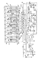
- the multi-flash lamp array of this invention which may comprise an insulating section 12 supporting ten reflectors 14A-14J comprising reflective recesses in which ten flash lamps 16A-16J are respectively mounted.
- Each of the flash lamps 16A-16J includes a pair of leads extending therefrom as shown at 28A-28J and 28A'-28J', respectively.
- the flash lamps 16A-16J are connected in pairs with one lead, 28A', 28C', 28E', 28G' and 281' from the respective first flash lamp of each pair being in common connection with a lead 28B', 28D', 28F', 28H' and 28J' from the second flash lamp of that pair.
- the flash lamp array 10 also includes a connector blade 30 depending from the insulating support section 12 and including a plurality of spaced apart terminal elements 24, 32, and 18A-18E. Each of the terminal elements 18A-18E connects, respectively, to the common leads 20A-20E of the flash lamp pairs.
- a common terminal element 24 is provided and connected to the leads 28A, 28C, 28E, 28G, and 281 of the first bulb of each pair by way of a common conductor 22.
- a flash actuated switch or fuse 26A-26E is stationed in close spaced-apart relation to each of the first flash lamps 16A, 16C, 16E, 16G and 161 of each pair.
- the switches 26A-26E may be heat responsive and may be provided with electrical contacts biased toward each other but held apart by a material which melts or deforms under the influence of the heat generated when a lamp is flashed to permit the contacts to close.
- the heat responsive material may be a material bridged between, or encapsulating, a pair of spaced apart terminals which is an insulator but becomes electrically conductive when heated by the associated flashing lamp.
- the flash actuated switches 26A-26E may also comprise light actuated switches of the type described in US-A-3,728,068.
- the flash actuated switches 26A-26E may be of any conventional type switch which is normally non-conductive and which responds to the ignition of the respective flash lamp by becoming conductive.
- the first flash actuated switch 26A operates to connect the lead 28B of the second flash lamp 16B of the first pair to the common conductor 22.
- the second flash actuated switch 26B operates to connect the lead 28D of the second lamp 16D of the second pair of lamps to the common line 22.
- the flash actuated switch 26B operates to connect the lead 28B of the second lamp 16B of the first pair of flash lamps to the common line 22.
- the flash actuated switch 26C operates to connect the other lead 28F from the second lamp 16F of the third pair to the common lead 22 while simultaneously connecting the other lead 28D of the second lamp 16D of the second pair to the common line 22.
- the remaining flash actuated switches 26D-26E operate in like manner simultaneously to connect the other lead of the second flash lamp of the same pair of lamps along with the other lead of the second flash lamps in the preceding pair of flash lamps to the common line 22.
- the connector blade 30 may be inserted into the receiving socket of a camera to connect with corresponding conductors from a typical flash fire sequencing circuit as shown generally at 34 which is disposed within the camera.
- the terminal element 32 on the connector blade 30 is wide to bridge a pair of conductors 36 and 38 in the flash sequencing circuit 34 thereby readying the flash sequencing circuit.
- the flash sequencing circuit 34 comprises five electronic switches. Of these, only three are shown, namely silicon controlled rectifiers SCR2, SCR3, and SCR6.
- the stage comprising the switch SCR3 is typical of the two stages between SCR3 and SCR6, which have not been shown.
- the anode terminals of the silicon controlled rectifiers SCR2-SCR6 connect, respectively, to the terminal elements 18A-18E when the array 10 is received in the camera socket. All the cathode terminals of the silicon controlled rectifiers connect to ground.
- the gates of the silicon controlled rectifiers SCR2-SCR6 connect to ground through a different one of a set of resistors R1o-R14 (only the resistors R10, R11 and R14 are shown).
- Each of the controlled rectifiers SCR2-SCR6 has its anode connected to the collector of a different NPN transistor Ql-Q5. The emitter of each transistor Ql-Q5 is connected to the gate of a different one of the silicon controlled rectifiers SCR2-SCR6.
- each transistor Ql-Q5 is connected to the collector of a different one of five inhibit NPN transistors Q6-Q10.
- the emitter of each of the transistors Q6-Q10 is grounded with respect to a battery 40.
- the base terminals of transistors Q6-Q10 are each connected through a different one of a series of current distributing resistors R15-R19 to an output terminal 42 of an electronic control module 44.
- each of the transistors Q6-Q10 is gated into conduction thereby preventing any of the transistors Ql-Q5 from being biased in conduction.
- the electronic control module 44 also provides a trigger signal at output terminal line 46 to the base of a PNP transistor Q11.
- the emitter terminal of transistor Q11 is connected to the positive voltage side of the battery 40 by way of a resistor R1 and a photographic cycle actuator button S1.
- the emitter terminal of transistor Q11 receives a positive potential from the battery 40 when the button S1 is depressed.
- the collector of the transistor Q11 is returned to ground through a resistor R20.
- the collector of transistor Q11 also connects to a lead 48 through a pair of diodes D4 and D5 in series.
- the lead 48 is connected to the base terminal of the transistor Q1 through a resistor R21.
- the lead 48 is also connected to the emitters of a group of four logic PNP transistors Q12-Q15, (only Q12 and Q15 are shown).
- the collectors of the transistors Q12-Q15 are connected to the bases of the transistors Q2-Q5, respectively.
- the base of the transistor Q12 is connected to the anode of the silicon controlled rectifier SCR2 through a resistor R22.
- a similar resistor R23 connects the anode of the silicon controlled rectifier SCR3 to the next stage transistor Q13, now shown. Further stages are similarly connected.
- the flash sequencing circuit 34 fires each flash lamp in a sequence advancing from first to last. This is accomplished by having each switching circuit receive a trigger signal only when the preceding flash lamp is open circuited. Assuming that none of the flash lamps have been fired and that the flash sequencing circuit 34 is triggered by the electronic control module 44, in response to depression of the actuator button S1, the trigger signal provides a zero or negative potential signal at output line 42 to maintain the inhibit transistors Q6-Q10 in a non-conducting state while a negative-going pulse is provided by the output terminal line 46 to gate transistor Q11 into conduction. Turning on transistor Q11 operates to render gate control transistor Q1 conductive to switch on SCR2 thereby coupling the first lamp 16A across the battery 40 to fire the lamp.
- SCR3 will not turn on because its gate control transistor Q2 remains non-conductive because its associated logic transistor Q12 is not rendered conductive. That is, the voltage across the emitter base junction of the transistor Q12 is substantially identical to the voltage across the flash lamp 16A and the latter voltage is low as the initial filament resistance is also low. However, as the lamp filament heats up, its resistance increases (just prior to opening of the filament) and the voltage across the lamp increases accordingly.
- the electronic control module 44 operates to turn on inhibit transistors Q6-Q10 so that subsequent circuits cannot turn on during a later time of the flashing of a preceding lamp. Thus, once firing of a bulb is initiated, a high level in each signal is provided from the flash sequencing circuit for feedback through the electronic control module 44 so that the distributor circuit 34 is clamped off to prevent additional lamps from firing at that time.
- Firing the lamp 16A operates to cause the switch 26A to close thereby connecting the lead 28B from the second flash lamp 16B of the first pair to the common lead 22.
- second flash lamp 16B becomes connected in parallel thereto by the switch 26A to that at the next photographic cycle, the SCR2 is triggered as before, now to fire the second lamp 16B of the first pair.
- the first SCR2 is conductive and the voltage across the first pair of open lamps 16A and 16B is high so that the voltage across the transistor Q12 exceeds the threshold necessary to turn on this transistor.
- the latter provides a suitable gating signal to the second SCR3 through gate transistor Q8 to draw ignition current through the first lamp 16C of the second pair of lamps.
- the following SCRs are not turned on as the transistor Q13 (not shown) is in parallel with the conducting line, and hence, is not biased into conduction.
- the firing of the flash lamp 16C operates to close the flash responsive switch 26B thereby connecting the lead 28D of the second flash lamp 16D of the second pair to the common line 22 while at the same time connecting the lead 28B of the second flash lamp 16B of the previously fired pair of flash lamps to the common terminal 22. Since lamp 16B may be expected to have been fired during the photographic cycle preceding the firing of lamp 16C, the connection of lead 28B to the common lead 22 by way of the flash responsive switch 26B has no effect on the order in which the flash lamps are fired. Therefore, the fourth photographic cycle would normally operate to effect the firing of lamp 16D by way of the silicon controlled rectifier SCR3 since the lamps 16A, 16B and 16C have already fired in the normal manner and are, thus, open circuited.
- the flash actuated switch 26A is not actuated to connect the lead 28B of the second flash lamp 16B of the first pair of flash lamps to the common lead 22. If the flash actuated switch 26A is defective it may fail to connect the lead 28B in the foregoing manner even if the first flash lamp 16A is not defective. In either case, a subsequent exposure operation which would have operated to fire the second flash lamp 16B in the first pair in the manner described instead operates to fire the first flash lamp 16C in the second pair.
- the flash actuated switch 26B precludes the loss of flash lamp 16B by:operating to connect the lead 28B to the common line 22.
- the flash lamp 16B is connected across the terminals 18A and 24 upon the firing of the first flash lamp 16C of the second pair regardless of whether the first flash lamp 16A of the first pair fires the switch 26A is defective.
- the next photographic exposure cycle after the flash lamp 16C is fired operates to fire the second flash lamp 16B of the first pair as the low impedance provided across the terminals 18A and 24 operates to preclude the gating on of transistor Q12.
- the next exposure cycle operates in the aforementioned manner to provide an ignition current to the second flash lamp 16D of the second flash lamp pair since the first and second flash lamps 16A and 16B of the first pair provide a high impedance that enables a high voltage across transistor Q12 to gate it on, and thereby provide an ignition current by way of SCR3 through the second flash lamp 16D of the second flash lamp pair.
- Each of the flash actuated switches 26B-26E provides a redundancy by operating to connect the second flash lamp in any previous flash lamp pair to the common conductor 22.
- the first flash lamp in the next succeeding pair of flash lamps operates to connect the second flash lamp of the preceding pair to the common line 22.
- the second flash lamp in that pair will not be lost but will be fired as a result of the redundant feature of the flash actuated switches 26A-26D.
- the detector arrangement may also be included a detector arrangement for examining the impedance of the last flash lamp 16J which is scheduled to be fired in the flash array 10.
- the detector arrangement embodies a differential type operational amplifier 50 having a pair of input terminals 52 and 51.
- Inputterminal 52 connects directly to the terminal strip 18E by way of interconnecting line 56 and is also grounded by way of a resistor R34.
- Input terminal 51 connects to the junction between a pair of resistors R30 and R32. The other side of resistor R32 is grounded while the other side of resistor R30 connects to the terminal 24 by way of interconnecting lines 58 and 60.
- resistor R30 Since terminals 18E and 24 connect to the last flash lamp scheduled to be fired, the resistance value of resistor R30 is selected to correspond with the predetermined impedance evidenced by a fully expended flash lamp (at least 75 ohms). Resistors R32 and R34 are configured to have substantially the same resistive values to define a voltage comparison network, the output of which at terminals 52 and 51 is amplified by the amplifier 50.
- the amplifier 50 is also coupled to the positive and negative terminals of battery 40 by means not shown.
- the output of amplifier 50 is connected to an inhibit and warn network 62 which may operate to provide both a warning signal to the user and an inhibit signal to the ECM 44 when the last flash lamp is expended.
- the output from the amplifier 50 may be considered “low” and the inhibit and warn network 62 allows normal operation of the ECM 44.
- the output of amplifier 50 reverts to an opposite level, for instance "high” to inhibit further camera operations.
Landscapes
- Physics & Mathematics (AREA)
- General Physics & Mathematics (AREA)
- Stroboscope Apparatuses (AREA)
- Discharge-Lamp Control Circuits And Pulse- Feed Circuits (AREA)
Claims (4)
Priority Applications (2)
| Application Number | Priority Date | Filing Date | Title |
|---|---|---|---|
| EP81305299A EP0078868B1 (fr) | 1981-11-06 | 1981-11-06 | Dispositif photographique à lampes flash |
| DE8181305299T DE3173836D1 (en) | 1981-11-06 | 1981-11-06 | Photographic flash lamp array |
Applications Claiming Priority (1)
| Application Number | Priority Date | Filing Date | Title |
|---|---|---|---|
| EP81305299A EP0078868B1 (fr) | 1981-11-06 | 1981-11-06 | Dispositif photographique à lampes flash |
Publications (2)
| Publication Number | Publication Date |
|---|---|
| EP0078868A1 EP0078868A1 (fr) | 1983-05-18 |
| EP0078868B1 true EP0078868B1 (fr) | 1986-02-19 |
Family
ID=8188446
Family Applications (1)
| Application Number | Title | Priority Date | Filing Date |
|---|---|---|---|
| EP81305299A Expired EP0078868B1 (fr) | 1981-11-06 | 1981-11-06 | Dispositif photographique à lampes flash |
Country Status (2)
| Country | Link |
|---|---|
| EP (1) | EP0078868B1 (fr) |
| DE (1) | DE3173836D1 (fr) |
Citations (1)
| Publication number | Priority date | Publication date | Assignee | Title |
|---|---|---|---|---|
| US3728068A (en) * | 1971-12-09 | 1973-04-17 | Gen Electric | Photoflash lamp array having flash-actuated switches |
Family Cites Families (3)
| Publication number | Priority date | Publication date | Assignee | Title |
|---|---|---|---|---|
| US3728947A (en) * | 1968-12-16 | 1973-04-24 | Gen Electric | Static electronic photoflash assembly and method of photoflash lighting |
| US3930184A (en) * | 1973-12-20 | 1975-12-30 | Polaroid Corp | Electronic flash coupling system for sequential flashbulb firing circuit |
| US3898512A (en) * | 1974-03-08 | 1975-08-05 | Berkey Photo Inc | Photoflash lamp array sequencing circuits |
-
1981
- 1981-11-06 EP EP81305299A patent/EP0078868B1/fr not_active Expired
- 1981-11-06 DE DE8181305299T patent/DE3173836D1/de not_active Expired
Patent Citations (1)
| Publication number | Priority date | Publication date | Assignee | Title |
|---|---|---|---|---|
| US3728068A (en) * | 1971-12-09 | 1973-04-17 | Gen Electric | Photoflash lamp array having flash-actuated switches |
Also Published As
| Publication number | Publication date |
|---|---|
| EP0078868A1 (fr) | 1983-05-18 |
| DE3173836D1 (en) | 1986-03-27 |
Similar Documents
| Publication | Publication Date | Title |
|---|---|---|
| US4064519A (en) | Regulated strobe for camera with sixth flash inhibit | |
| US3858227A (en) | Adapter apparatus for flash firing system | |
| US3618492A (en) | Flash photographic system | |
| EP0078868B1 (fr) | Dispositif photographique à lampes flash | |
| US4097220A (en) | Flash lamp array having shorting lamps | |
| US4329140A (en) | Multiple flash arrangement with redundant fuse arrangement | |
| CA1091205A (fr) | Indicateur de dernier eclair pour ensemble de lampes- eclairs | |
| US4074295A (en) | Compact accessory strobe for cameras with battery enclosed film pack | |
| CA1151720A (fr) | Flash a lampes multiples avec dispositif de fusionnement redondant | |
| US3601652A (en) | Slave flash light | |
| US3895265A (en) | Sequencing circuit for firing photoflash lamps in predetermined order | |
| US3728067A (en) | Device for flashing combustion flash bulbs one after the other | |
| US3898512A (en) | Photoflash lamp array sequencing circuits | |
| CA1111899A (fr) | Indicateur-interrupteur d'epuisement de la reserve de lampes-eclair groupees | |
| US3758822A (en) | Computer type flash apparatus with noise inhibiting quench circuit | |
| US3728068A (en) | Photoflash lamp array having flash-actuated switches | |
| US4334856A (en) | Photoflash array with selective pairing of lamps | |
| US3864606A (en) | Compensated sequencing circuit for firing photoflash lamps | |
| EP0081735B1 (fr) | Dispositif de flash multiple avec circuit pour la commutation redondante de lampes | |
| US4324543A (en) | Photoflash array with selective pairing of lamps and switching of common circuit | |
| US3726631A (en) | Device for the consecutive ignition of combustion flash-light lamps | |
| US3787167A (en) | Current-sensing circuit for determining flashing of a photoflash lamp | |
| US3860856A (en) | Latching circuitry in a circuit for sequentially firing photoflash lamps | |
| JPS5888730A (ja) | 多ランプ写真フラツシユアレイ | |
| US3993929A (en) | Automatic correct exposure indicator |
Legal Events
| Date | Code | Title | Description |
|---|---|---|---|
| PUAI | Public reference made under article 153(3) epc to a published international application that has entered the european phase |
Free format text: ORIGINAL CODE: 0009012 |
|
| AK | Designated contracting states |
Designated state(s): DE FR GB IT NL |
|
| 17P | Request for examination filed |
Effective date: 19831102 |
|
| GRAA | (expected) grant |
Free format text: ORIGINAL CODE: 0009210 |
|
| AK | Designated contracting states |
Designated state(s): DE FR GB IT NL |
|
| ET | Fr: translation filed | ||
| REF | Corresponds to: |
Ref document number: 3173836 Country of ref document: DE Date of ref document: 19860327 |
|
| ITF | It: translation for a ep patent filed | ||
| PLBE | No opposition filed within time limit |
Free format text: ORIGINAL CODE: 0009261 |
|
| STAA | Information on the status of an ep patent application or granted ep patent |
Free format text: STATUS: NO OPPOSITION FILED WITHIN TIME LIMIT |
|
| 26N | No opposition filed | ||
| PGFP | Annual fee paid to national office [announced via postgrant information from national office to epo] |
Ref country code: NL Payment date: 19871130 Year of fee payment: 7 |
|
| PG25 | Lapsed in a contracting state [announced via postgrant information from national office to epo] |
Ref country code: GB Effective date: 19881106 |
|
| GBPC | Gb: european patent ceased through non-payment of renewal fee | ||
| PG25 | Lapsed in a contracting state [announced via postgrant information from national office to epo] |
Ref country code: FR Free format text: LAPSE BECAUSE OF NON-PAYMENT OF DUE FEES Effective date: 19890731 |
|
| PG25 | Lapsed in a contracting state [announced via postgrant information from national office to epo] |
Ref country code: DE Effective date: 19890801 |
|
| REG | Reference to a national code |
Ref country code: FR Ref legal event code: ST |
|
| PG25 | Lapsed in a contracting state [announced via postgrant information from national office to epo] |
Ref country code: NL Effective date: 19900601 |
|
| NLV4 | Nl: lapsed or anulled due to non-payment of the annual fee |