EP0085451A1 - Circuit-IF de télévision - Google Patents
Circuit-IF de télévision Download PDFInfo
- Publication number
- EP0085451A1 EP0085451A1 EP83200073A EP83200073A EP0085451A1 EP 0085451 A1 EP0085451 A1 EP 0085451A1 EP 83200073 A EP83200073 A EP 83200073A EP 83200073 A EP83200073 A EP 83200073A EP 0085451 A1 EP0085451 A1 EP 0085451A1
- Authority
- EP
- European Patent Office
- Prior art keywords
- input
- sound
- signal
- balanced
- circuit
- Prior art date
- Legal status (The legal status is an assumption and is not a legal conclusion. Google has not performed a legal analysis and makes no representation as to the accuracy of the status listed.)
- Granted
Links
- 230000005236 sound signal Effects 0.000 claims abstract description 75
- 239000011159 matrix material Substances 0.000 claims abstract description 62
- 230000001360 synchronised effect Effects 0.000 claims description 6
- 230000001629 suppression Effects 0.000 description 6
- 239000000969 carrier Substances 0.000 description 5
- 238000010586 diagram Methods 0.000 description 5
- 238000000926 separation method Methods 0.000 description 5
- 238000001514 detection method Methods 0.000 description 4
- 230000003321 amplification Effects 0.000 description 3
- 238000006243 chemical reaction Methods 0.000 description 3
- 230000003412 degenerative effect Effects 0.000 description 3
- 238000003199 nucleic acid amplification method Methods 0.000 description 3
- 239000000654 additive Substances 0.000 description 2
- 230000000996 additive effect Effects 0.000 description 2
- 238000004519 manufacturing process Methods 0.000 description 2
- 238000000034 method Methods 0.000 description 2
- 239000003990 capacitor Substances 0.000 description 1
- 239000003795 chemical substances by application Substances 0.000 description 1
- HPNSNYBUADCFDR-UHFFFAOYSA-N chromafenozide Chemical compound CC1=CC(C)=CC(C(=O)N(NC(=O)C=2C(=C3CCCOC3=CC=2)C)C(C)(C)C)=C1 HPNSNYBUADCFDR-UHFFFAOYSA-N 0.000 description 1
- 238000010276 construction Methods 0.000 description 1
- 230000000694 effects Effects 0.000 description 1
- 230000010354 integration Effects 0.000 description 1
- 238000011031 large-scale manufacturing process Methods 0.000 description 1
Images


Classifications
-
- H—ELECTRICITY
- H04—ELECTRIC COMMUNICATION TECHNIQUE
- H04N—PICTORIAL COMMUNICATION, e.g. TELEVISION
- H04N5/00—Details of television systems
- H04N5/44—Receiver circuitry for the reception of television signals according to analogue transmission standards
- H04N5/60—Receiver circuitry for the reception of television signals according to analogue transmission standards for the sound signals
Definitions
- the invention relates to a TV-IF circuit comprising a balanced video signal path arranged between an IF-input and a video signal output, and a balanced sound signal path arranged between the IF-input and a sound signal output, these paths including a video mixing stage and a sound mixing stage, respectively.
- Such a TV-IF circuit is known as a TV-IF circuit for quasi-parallel sound processing and is described in the publication "Hartung des thoroughlytonsignals mit den dichen GmbH TDA 2545 und TDA 2546 nach dem Quasi-Paralleltonmaschine" published in the series “Valvotechnischsmitteilungen", November 1980.
- An IF-TV signal applied to the known TV-IF circuit is separated therein into a video and a sound signal.
- the TV-IF circuit comprises two filter circuits, connected to the IF-input, one filter circuit suppressing the sound carrier of the TV-IF signal and being included in the video signal path and the other filter circuit suppressing the video information with the exception of the picture carrier and being included in the sound signal path.
- the video signal path contains vitually no sound signal compoenents which may disturb the video signal after demodulation in the video mixing stage and the sound signal path contains virtually no video signal components which may disturb the sound signal after intercarrier mixing of the sound carrier and the picture carrier in the sound mixing stage.
- the frequency of the sound signal modulated on the sound carrier is converted into a sound intermediate frequency which corresponds to the picture-sound carrier spacing in the TV-IF signal.
- the IF-sound signal thus obtained is not affected by unwanted frequency shifts of the tuning oscillator.
- the whole TV-IF signal is applied to the video mixing stage. Thereafter mixing of the TV-IF signal with the picture carrier is effected in the video mixing stage, as a result of which the demodulation of the video signal and simultaneously a conversion of the sound signal frequency into the said sound intermediate frequency is obtained in response to an intercarrier mixing of the sound carrier and the picture carrier.
- the demodulated video signal and the IF sound signal are both available here at the same output of the video detector for further signal processing and, because of the common mixing in the video mixing stage, each of the two signals comprises residual components of the other signal.
- TV-IF circuits for quasi-parallel sound processing are mainly used in TV-receivers which must satisfy high quality requirements as regards picture display and sound reproduction.
- high-quality TV-receivers are generally comparatively expensive and are only sold in a limited number. Consequently, the production of TV-IF circuits for quasi-parallel sound processing is limited.
- the circuit itself if rather complicated such circuits are in the present state of the art much more expensive than TV-IF circuits for intercarrier sound processing.
- the TV-IF circuits for intercarrier sound processing are less complicated and particularly suitable for use in TV-receivers on which lower quality requirements are imposed.
- the lower quality requirements make it possible to use for the entire TV-receiver simple and cheap receiver circuits so that TV-receivers of this type can be much cheaper than the first-mentioned high-quality TV-receivers.
- the demand for the cheap TV-receivers is comparatively high and consequently also the production of the last-mentioned TV-IF circuits.
- the invention has for its object to increase the suitability for use of the known TV-IF circuits for quasi-parallel sound processing by making these TV-IF circuit compatable with TV-IF circuits for intercarrier sound processing and on the other hand to provide a possibility to simplify the circuit and to improve the suppression of unwanted signal components in both signal paths.
- a TV-IF circuit of the type described in the opening paragraph is characterized by a matrix circuit having a balanced, non-inverting and a balanced, inverting input, as well as a balanced output, this matrix circuit being included via its non-inverting input and its output in one of the two said signal paths between the IF-input and a signal input of the mixing stage in this signal path, the other signal path between the IF-input and a signal input of the mixing stage in the said other signal path being connected to the balanced, inverting input of the matrix circuit ans comprising between the IF-input and the matrix circuit a balanced first pair of terminals which may optionally be shortcircuited, remain open-circuited or for connecting therebetween a resonant circuit having a resonant frequency which corresponds to a sound carrier frequency of the TV-IF signal applied to the IF-input.
- the use of the measure in accordance with the invention provides by connected or not connecting a resonant circuit between said balanced first pair of terminals the possibility for a quasi-parallel or an intercarrier signal processing in the TV-IF circuit in accordance with the invention.
- the TV-TF circuit in accordance with the invention is consequently suitable for use in both the more expensive high-quality TV-receivers and the TV-receivers on which less stringent quality requirements are imposed. A large scale production of such TV-IF circuits is therefore possible. As a result thereof the price per unit can be lower than the unit price of prior art TV-IF circuits.
- the use of the measure in accordance with the invention when the TV-IF circuit in accordance with the invention is used for a quasi-parallel sound processing, results in that by the use of one resonant circuit both the sound signal components in the video signal path and the video signal components in the sound signal path can be suppressed.
- a preferred embodiment of a TV-IF circuit in accordance with the invention is characterized in that the matrix circuit is included in the video signal path and the balanced first pair of terminals is included in the sound signal path, this first pair of terminals being shortcircuited or interconnected via a resonant circuit having a band rejection characteristic.
- a further preferred embodiment of a TV-IF circuit in accordance with the invention is characterized by a further balanced sound signal path an input of which is connected, via a further balanced pair of terminals for connecting therebetween a band rejection resonant circuit having a resonant frequency which corresponds to a further sound carrier frequency of the TV-IF signal being applied to the IF-input, to a further sound mixing stage, said input of the further sound signal path on the other hand being connected to the output of the matrix circuit and on the other hand via the further pair of terminals to an inverting input of a further matrix circuit, which further matrix circuit is connected via a non-inverting input to the IF-input and via an output to the video mixing stage.
- This measure can be used with special advantage in the processing of more than one sound signal as it results in a significant reduction the mutual crosstalk between the sound signals to be processed.
- a further preferred embodiment of such a TV-IF circuit in accordance with the invention is characterized by a push-pull amplifier connected to the IF-input, the output of this amplifier being connected to the balanced first pair of terminals and also to the base input of a balanced first pair of transistors, as well as by a balanced second pair of transistors also connected to the IF-input, the emitter output of the first transistor pair being connected via the matrix circuit to the collector output of the second transistor pair, which matrix circuit comprises two resistors which crosswise connect said emitter output of the first transistor pair to said collector output of the second transistor pair, also comprising a resistor which interconnects said two resistors.
- the video signal path A 5 , M, A 6 , VM comprises a matrix circuit M having a balanced, inverting and a balanced non-inverting input with terminals 4, 4' and 5, 5', respectively and a balanced output with terminals 6 and 6', as well as a synchronous video detector VM having a balanced signal input with terminals 7 and 7', a balanced carrier input with terminals 8 and 8' and a signal output connected to the video output 2, 2'.
- the IF-input 1, 1' is connected via an amplifier A 5 to the non-inverting input 5, 5' of the matrix circuit M, while the output 6, 6' of the matrix circuit M is connected to the signal input 7, 7' of the video detector VM via an amplifier A 6 .
- the sound signal path A 1 , A 2 , A 79 SM comprises a first balanced terminal pair 9, 9' between which a resonant circuit FSC is arranged when the TV-IF circuit is used for a quasi-parallel sound processing.
- This resonant circuit FSC has a resonant frequency which corresponds to the sound carrier frequency (33,4 MHz) of the TV-IF signal applied to the IF-input 1, 1'.
- the sound signal path A 1 , A 2 , A 7 , Sm also comprises a sound mixing stage SM having a balanced signal input with terminals 10 and 10', a balanced carrier input with terminals 11 and 11' and a balanced output, which is connected to the sound signal output 3, 3'.
- the IF-input 1, 1' is connected to the first terminal pair 9, 9' via a buffer amplifier A1 .
- the first terminal pair 9, 9' is further connected via a buffer amplifier A 2 on the one hand via an amplifier A 7 to the signal input 10, 10' of the sound mixing stage SM an on the other hand to the inverting input 4, 4' of the matrix circuit M.
- the balanced output 6, 6' of the matrix circuit M is connected via a buffer amplifier A 3 to a balanced second terminal pair 12, 12' between which a resonant circuit FVC is also connected when the TV-IF circuit is used for quasi-parallel sound processing.
- the resonant circuit FVC has a resonant frequency which is equal to the picture carrier frequency (38.9 MHz) of the TV-IF signal to be processed.
- the second terminal pair 12, 12' is connected via an amplifier A. to the carrier input 11, 11' of the sound detector SM, and via an amplifier A 8 to the carrier input 8, 8' of the video detector VM.
- the amplifiers A4 to A 8 , inclusive are predominantly used to set a proper signal amplitude
- the buffer amplifiers A 1 to A3, inclusive are predominantly used as separation stages to prevent, for example, a mutual shortcircuit- ing of the first terminal pair 9, 9' or of the second terminal pair 12, 12' from resulting in an unwanted shortcir- cuiting of the signal path connected in parallel therewith.
- a detailed description of the function of these amplifiers A 1 to A 89 inclusive is not necessary for an understanding of the invention and is therefore omitted for the sake of clarity.
- a TV-IF signal applied to the IF-input 1, 1' is wholly applied to the non-inverting signal input 5, 5' of the matrix circuit M after adequate amplification in the amplifier A 5 on the one hand and on the other hand, after having passed through the buffer amplifier A when the TV-IF circuit is used for a quasi-parallel sound processing is filtered in the resonant circuit FSC which is arranged between the two first pair of terminals 9, 9'.
- the resonant circuit FSC is tuned to the sound carrier frequency (33.4 MHz) of the TV-IF signal to be processed and realizes a very high impedance for frequencies at and near this sound carrier frequency and a low impedance to substantially a shortcircuit for the other frequencies.
- the resonant circuit FSC may be of a simple construction, for ecample in the form of a parallel LC circuit as shown in the drawing.
- the resonant circuit FSC effects a selection of the sound signal, modulated on the sound carrier, from the TV-IF signal, which sound signal after passing the buffer amplifier A 2 is applied to the inverting signal input 4, 4' of the matrix circuit M and also, after adequate amplification in the amplifier A 7 to the signal input 10, 10' of the sound detector SM.
- the sound signal applied to the inverting signal input 4, 4' is subtracted from the total TV-IF signal applied to the non-inverting signal input 5, 5'.
- the video signal that is to say the TV-IF signal with suppressed sound carrier is available at the output 6, 6' of the matrix circuit M with the same polarity as the TV-IF signal at the non-inverting signal input 5, 5'.
- This video signal is applied after adequate amplification in the amplifier A 6 to the signal input 7, 7' of the video detector VM and also, after passing the buffer amplifier A3, to the second pair of terminals 12, 12'.
- the resonant circuit FVC arranged between this pair of terminals 12, 12 t is tuned to the picture carrier frequency (38.9 Hz) and realizes a very high impedance for frequencies at and near the picture carrier frequency (38.9 MHz) and a low impedance to substantially a shortcircuit for the other frequencies.
- the picture carrier is filtered from the video signal applied to the pair of terminals 12, 12', which picture carrier is applied to the picture carrier input 11, 11' of the sound mixing stage SM via the amplifier A and to the picture carrier input 8, 8 t of the video mixing stage VM via the amplifier A 8 1
- the intercarrier of the modulated 33.4 MHz sound carrier applied to the signal input 10, 10' and the 38.9 MHz picture carrier applied to the picture carrier input 11, 11' are mixed.
- a 5.5 MHz IF-sound signal is obtained at the sound signal output 3, 3', which sound signal is processed in a sound detector, not shown, into an audio-frequency mono or stereophonic sound signal.
- a synchronous detection of the video-signal occurs which video signal is available in the basic frequency band at the video output 2, 2' for further processing in a video output stage, not shown.
- the sound signal is quasi parallel processed.
- the separation between the sound and the video signals required therefor is achieved by means of the matrix circuit M and a simple resonant circuit FSC, which may be in the form of a simple parallel LC or RLC network.
- FSC simple resonant circuit
- the amplifier A 5 By means of a proper mutual adjustment of the signal amplitudes of the sound signal and the complete TV-IF signal at the input terminals 4, 4' and 5, 5', respectively by means of the amplifier A 5 , and, optionally, the buffer amplifier A a full suppression of the sound signal in the video signal can further be obtained.
- the selection of the picture carrier is effected by means of a simple resonant circuit FVC, which, as the resonant circuit FSC, may be in the form of a single parallel LC or RLC network.
- FVC simple resonant circuit
- the selection of the picture carrier from the video signal is a guarantee that no residual components of the sound signal are present in the picture carrier signal at the picture carrier inputs 8, 8' and 11, 11' of the video mixing stage VM and the sound mixing stage SM, respectively, which residual components might have a disturbing influence on the output signal of these mixing stages.
- the first pair of terminals 9, 9' must first be mutually shortcircuited, which results in no signal being applied to the sound mixing stage SM, while there is also no signal at the inverting signal input 4, 4' of the matrix circuit M.
- the sound mixing stage SM is inoperative and does not supply a signal at its signal output 3, 3'.
- the TV-IF signal applied to the IF-input 1, 1' passes completely through the amplifier A 5 , the matrix circuit M and the amplifier A 6 and is demodulated in accordance with the intercarrier method in the video mixing stage VM. If a synchronous demodulation is desired then in the resonance circuit FVC arranged between the second pair of terminals 12, 12' the picture carrier is selected from the TV-IF signal being applied via the signal output 6, 6' of the matrix circuit M, which picture carrier is applied to the picture carrier input 8, 8' of the video mixing stage VM, which now operates as a multiplicative stage. A multiplicative intercarrier mixing of the modulated sound carrier with the picture carrier and simultaneously a synchronous detection of the video signal then taking place in the video mixing stage VM. Thus, both the 5.5 MHz IF-sound signal and the baseband video signal are then available at the video output 2, 2' for further signal processing in sound and video output stages not shown.
- the second pair of terminals 12, 12' can be mutually shortcircuited.
- an additive intercarrier mixing of the modulated sound carrier with the detector carrier and simultaneously a non-linear detection of the video signal takes place, so that at the vieo output 2, 2' again both the 5.5 MHz IF-sound signal and the baseband video signal are available for further signal processing, not shown.
- FIG 2 shows a second embodiment of a TV-IF circuit in accordance with the invention, the elements which correspond to the elements of the TV-IF circuit of Figure 1 are given the same reference numerals.
- the video signal path then comprises the first pair of terminals 9, 9' between the IF-input 1, 1' and the video mixing stage VM, and between the first pair of terminals 9, 9' and the video mixing stage VM the video signal path being connected to the inverting input 4, 4' of the matrix circuit M.
- the sound signal path comprises the matrix circuit M, the non-inverting input 5, 5' thereof being connected via the amplifier A 5 to the IF-input 1, 1', and the output 6, 6' thereof via the amplifier A to the signal input 10, 10' of the sound mixing stage SM.
- the selection of the video signal is effected by suppressing by means of the series resonant circuit FSC the modulated sound carrier of the TV-IF signal applied to the first pair of terminals 9, 9' via the buffer amplifier A 1 .
- This series resonant circuit FSC 1 realizes a low impedance to substantially a shortcircuit for frequencies at and near the sound carrier and a high impedance for other frequencies.
- the video signal is applied via the amplifier A 2 to on the one hand the inverting input 4, 4' of the matrix circuit M, and subtracted therein from the complete TV-IF signal being applied via the amplifier A 5 to the non-inverting input 5, 5' of the matrix circuit M, and on the other hand to the video mixing stage VM via the amplifier A G .
- the output 6, 6' of the matrix circuit M the sound signal which is applied to the signal input 10, 10' of the sound mixing stage SM via the amplifier A 7 .
- the video signal at the first pair of terminals 9, 9' is also applied via the amplifiers A and A3 to the second pair of terminals 12, 12', where by means of the parallel 38.9 MHz resonant circuit FVC the 38.9 MHz picture carrier is selected.
- this picture carrier is applied via the amplifier A4 to the carrier input 11, 11' of the sound mixing stage VM and via the amplifier A 8 to the carrier input 8, 8' of the video mixing stage VM, respectively, where in the manner described in the foregoing a synchronous detection of the video signal and intercarrier mixing, respectively of the modulated 33.4 MHz sound carrier and the 38.9 MHz picture carrier is effected.
- the baseband video signal is available at the video output 2, 2' and the 5.5 MHz IF-sound signal at the sound output 3, 3' for further processing in video and sound output stages, not shown.
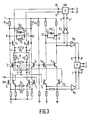
- FIG 3 shows a practical embodiment of the TV-IF circuit of Figure 1, which is particularly suitable for integration.
- the IF-TV circuit of Figure 3 comprises two cascode-arranged pairs of transistors T 1 , T 2 and T 31 T 4' whose operation is similar to that of the amplifier A of Figure 1.
- the balanced base input of the pair of transistors T 1 , T 2 is connected to the IF-input 1, 1'
- the base input of the pair of transistors T 39 T 4 is connected to a fixed operating voltage and its collector output is connected to a supply voltage via collector resistors R 1A and R 1B , r e s- pectively and comprises the first pair of terminals 9, 9'.
- a resistor R 1C is arranged between the said collector resistors R 1A and R 1B and in association with these two collector resistors and with a degenerative resistor R 7 arranged between the emitters of the pair of transistors T 1' T 2 serves for a first setting of the gain of the amplifier T 1 - T 4 (A 1 ).
- the resonant circuit FSC formed by a parallel network R 1 L 1 C 1 is arranged between the pair of terminals 9, 9' and is tuned to the 33.4 MHz sound carrier of the TV-IF signal to be processed.
- the resistor R ia variable is used for a fine setting of the gain of the amplifier T 1 - T 4 (A 1 ) for a correct subtraction in the matrix circuit M, which will be described in detail hereinafter.
- the pair of terminals 9, 9 1 is also connected to the base input of a balanced pair of transistors T 7 , T 8 , in which the 33.4 MHz sound signal selected with the resonant circuit FSC is amplified.
- the operation of the pair of transistors T 79 T 8 from the base input to the emitter input is similar to the amplifier A 2 and from the base input to the collector output is similar to the combination of amplifiers A 2 and A 7 of Figure 1.
- the emitter output of the pair of transistors T 7 , T 8 are interconnected via a degenerative resistor R 2 , and are also connected to the inverting input 4, 4' of the matrix circuit M and the collector output to the signal input 10, 10' of the sound mixing stage SM.
- the IF-input 1, 1' is also connected to the base input of a balanced pair of transistors T 5 , T 6 , which form the amplifier A 5 of Figure 1.
- the collector output of the pair of transistors T 5 , T 6 is connected to the non-inverting input 5, 5' of the matrix circuit M.
- the emitter outputs of the pair of transistors T 5 , T 6 are interconnected via a degenerative resistor R 6 , which resistor R 6 determines in association with resistors R 3 - R 5 , still to be described hereinafter, of the matrix circuit M the gain of the amplifier T 5 , T 6 (A 5 ).
- the matric circuit M comprises a resistance network R 3 to R 5 , inclusive, the balanced emitter output of the pair of transistors T 7 , T 8 being crosswise coupled via the resistors R 3 and R 5 to the balanced collector output of the pair of transistors T 5 , T 6 , the resistor R 4 being arranged between the collector input.
- the 33.4 MHz sound signal amplified by the pair of transistors T 7 , T 8 is subtracted from the complete TV-IF signal which is amplified by the pair of transistors T 5 , T 6 .
- the result of this subtraction i.e. the video signal, is available at the non-inverting input 5, 5' of the matrix circuit M, as a result of which the non-inverting input 5, 5' embodies in the embodiment shown at the same time the output 6, 6' of the matrix circuit M.
- the video signal is coupled to the base input of a balanced pair of transistors T 9 , T 10 , which is arranged in cascode with a pair of transistors T 11 , T 12 and forms in combination therewith the amplifier A3 of Figure 1.
- the bases of the pair of transistors T 11 and T 12 are connected to the beforementioned fixed operating voltage, to which also the bases of the pair of transistors T 3 , T 4 are connected.
- the balanced collector of the pair of transistors T 11 , T 12 comprise the second pair of terminals 12, 12' between which the resonant circuit FVC is connected.
- the resonant circuit FVC is formed by a parallel network L 2 C2which is tuned to the 38.9 MHz.picture carrier frequency of the TV-IF signal to be processed.
- the 38.9 MHz picture carrier which, as shown in Figure 1, is applied via the amplifier A4 to the picture carrier input 11, 11' of the sound mixing stage SM and also, via the amplifier A 8 to the picture carrier input 8, 8' of the video mixing stage VM is available at the second pair of terminals 12, 12'.
- the operation of the pair of transistors T 9 , T 10 from the base input to the emitter output is similar that of the amplifier A 6 of Figure 1, by means of which the video signal at the output 6, 6' of the matrix circuit M is amplified and applied to the signal input 7, 7' of the video mixing stage VM.
- the first pair of terminals 9, 9' must be mutually shortcircuited and both the video - baseband signal and the 5.5 MHz intermediate-frequency sound signal are available at the video output 2, 2' of the video mixing stage VM for further signal processing.
- the resistors R 1 to R 71 inclusive had the following resistance values 10K ⁇ , 150 ⁇ , 1K ⁇ , 1K ⁇ , 1K ⁇ , 520 ⁇ and 235 ⁇ , respectively; the resistors R 1A , R 1B and R 1C the values 5K , 5K and 6.5K , respectively; the coils L 1 and L 2 the values 0.6 / uH and 0.17 / uH, respectively and the capacitors C 1 and C 2 the values 39 / uF and 100 pF, respectively.
- the embodiments described so far can be simply adapted for processing TV-IF signals having two sound carriers, which are located at, for example, the frequencies of 37.14 MHz and 33.4 MHz. This is, for example, accomplished by chosing the resonant frequency of the resonant circuits FSC and FSC' to be located between the two sound carrier frequencies, for example at 33.27 MHz and by adjusting the quality factor sufficiently low to select the two sound carriers simultaneously from the complete TV-IF signal. A frequency conversion is then effected simultaneously in the sound mixing stage SM for the two sound carriers by multiplication by the 38.9 MHz picture carrier, one sound carrier being converted to a sound intermediate frequency of 5.5. MHz and the other sound carrier to a sound intermediate frequency of 5.74 MHz.
- the sound intermediate frequency signals thus obtained are thus both available at the sound output 3, 3' and can be separated from each other after selection and de demodulated separately by means of frequency demodulators, not shown, into audio-frequency sound signals.
- FIG 4 shows a block circuit diagram-.of a TV-IF circuit in accordance with the invention, in which elements corresponding to the elements of the TV-IF circuit shown in Figure 1 have been given the same references.
- a serial selection or suppression, respectively of the two sound signals is effected from or in, respectively the complete TV-IF signal.
- This selection or suppression respectively corresponds for each of the two sound signals to those as regards the sound signal in the TV-IF circuit of Figure 1.
- a circuit formed by A 1 ', A 2 ', A 5 ', FSC' and M' is arranged between the matrix circuit M and the amplifier A3, which circuit corresponds to the circuit formed by A A 2 A 5 FSC and M.
- the resonant circuits FSC and FSC' are tuned to the carrier frequencies 33.4 MHz and 33.14 MHz, respectively of the two sound signals.
- the 38.9 MHz picture carrier selected by means of the resonant circuit FVC consequently comprises substantially no components of the sound signals, so that, in addition, an interference-free demodulation or frequency conversion, respectively of the video signal or the two sound signals, respectively is ensured.
- FIG. 5 shows a block circuit diagram of a TV-IF circuit in accordance with the invention in which the elements corresponding to the elements of the TV-IF circuit shown in Figure 4 have been given the same references.
- a mutually separate, parallel selection of the two sound signals from the complete TV-IF signal is effected.
- crosstalk between the two sound signals is prevented from occurring.
Landscapes
- Engineering & Computer Science (AREA)
- Multimedia (AREA)
- Signal Processing (AREA)
- Television Receiver Circuits (AREA)
Applications Claiming Priority (2)
| Application Number | Priority Date | Filing Date | Title |
|---|---|---|---|
| NL8200328 | 1982-01-29 | ||
| NL8200328A NL8200328A (nl) | 1982-01-29 | 1982-01-29 | Tv-mf schakeling. |
Publications (2)
| Publication Number | Publication Date |
|---|---|
| EP0085451A1 true EP0085451A1 (fr) | 1983-08-10 |
| EP0085451B1 EP0085451B1 (fr) | 1985-05-02 |
Family
ID=19839156
Family Applications (1)
| Application Number | Title | Priority Date | Filing Date |
|---|---|---|---|
| EP83200073A Expired EP0085451B1 (fr) | 1982-01-29 | 1983-01-19 | Circuit-IF de télévision |
Country Status (8)
| Country | Link |
|---|---|
| US (1) | US4528592A (fr) |
| EP (1) | EP0085451B1 (fr) |
| JP (1) | JPS58134585A (fr) |
| AU (1) | AU551196B2 (fr) |
| CA (1) | CA1214544A (fr) |
| DE (1) | DE3360144D1 (fr) |
| ES (1) | ES519310A0 (fr) |
| NL (1) | NL8200328A (fr) |
Families Citing this family (3)
| Publication number | Priority date | Publication date | Assignee | Title |
|---|---|---|---|---|
| EP0349660B1 (fr) * | 1988-07-02 | 1993-10-06 | Deutsche ITT Industries GmbH | Circuit de conversion de fréquence pour un canal de télévision |
| FR2658302B1 (fr) * | 1990-02-13 | 1992-07-24 | Thomson Lgt | Procede, et dispositif, de mesure unique pour visualiser et qualifier la linearite d'une chaine de transmission. |
| JP2008038440A (ja) * | 2006-08-04 | 2008-02-21 | Tsuchiya Tsco Co Ltd | 隙間材 |
Family Cites Families (4)
| Publication number | Priority date | Publication date | Assignee | Title |
|---|---|---|---|---|
| NL7908216A (nl) * | 1979-11-09 | 1981-06-01 | Philips Nv | Televisie-ontvanger voor het ontvangen van een met een videosignaal amplitudegemoduleerde beelddraaggolf en van een met een audiosignaal frekwentiegemoduleerde geluidsdraaggolf. |
| JPS57127367A (en) * | 1981-01-30 | 1982-08-07 | Sony Corp | Receiver of television sound signal |
| US4395735A (en) * | 1981-08-31 | 1983-07-26 | Rca Corporation | FM Counter detector |
| US4470071A (en) * | 1982-08-30 | 1984-09-04 | Rca Corporation | Television sound detection system using a frequency translation phase-locked loop |
-
1982
- 1982-01-29 NL NL8200328A patent/NL8200328A/nl not_active Application Discontinuation
-
1983
- 1983-01-19 DE DE8383200073T patent/DE3360144D1/de not_active Expired
- 1983-01-19 EP EP83200073A patent/EP0085451B1/fr not_active Expired
- 1983-01-24 US US06/460,414 patent/US4528592A/en not_active Expired - Fee Related
- 1983-01-26 AU AU10774/83A patent/AU551196B2/en not_active Ceased
- 1983-01-27 CA CA000420369A patent/CA1214544A/fr not_active Expired
- 1983-01-27 ES ES519310A patent/ES519310A0/es active Granted
- 1983-01-28 JP JP58012579A patent/JPS58134585A/ja active Pending
Non-Patent Citations (1)
| Title |
|---|
| NACHRICHTEN ELEKTRONIK, vol. 35, no. 4, 1981, pages 157-163, Heidelberg (DE); * |
Also Published As
| Publication number | Publication date |
|---|---|
| NL8200328A (nl) | 1983-08-16 |
| US4528592A (en) | 1985-07-09 |
| JPS58134585A (ja) | 1983-08-10 |
| DE3360144D1 (en) | 1985-06-05 |
| CA1214544A (fr) | 1986-11-25 |
| EP0085451B1 (fr) | 1985-05-02 |
| AU551196B2 (en) | 1986-04-17 |
| ES8400840A1 (es) | 1983-11-01 |
| AU1077483A (en) | 1983-08-04 |
| ES519310A0 (es) | 1983-11-01 |
Similar Documents
| Publication | Publication Date | Title |
|---|---|---|
| US4974087A (en) | Parallel sound if with reference carrier derived from quasi-synchronous video detector | |
| AU638797B2 (en) | Quasi-parallel if with shared saw filter | |
| US4528592A (en) | TV-IF Circuit | |
| GB1575261A (en) | Television sund system | |
| US20030156228A1 (en) | Radio frequency modulator having C/L delay compensation function, and set-top-box using the same | |
| CA1250947A (fr) | Recepteur de television a entree video auxiliaire | |
| JPS6323408A (ja) | 二重目的の可変qフイルタ装置 | |
| US4513323A (en) | Buzz reduction for intercarrier type television sound detection | |
| JPS61248682A (ja) | 映像信号処理表示装置 | |
| US4516153A (en) | Composite video signal processing apparatus providing amplitude equalization | |
| JP4620872B2 (ja) | If信号処理装置 | |
| US4630119A (en) | Sound detecting circuit | |
| JP2596726B2 (ja) | 準並列テレビジヨンif段 | |
| US4376953A (en) | Signal separation networks | |
| JP2515086Y2 (ja) | 映像中間周波処理回路 | |
| KR910002240Y1 (ko) | 색도 신호와 휘도 신호의 간섭 방지회로 | |
| KR930004656Y1 (ko) | Tv의 중간주파신호처리시스템 | |
| JP2735832B2 (ja) | テレビジョン音声多重復調回路 | |
| US4283741A (en) | Signal separation networks | |
| JP3526195B2 (ja) | Secamクロマフィルタ回路 | |
| JPH06189271A (ja) | 拡張テレビジョン信号受信装置 | |
| JP3526194B2 (ja) | Secamカラー判別回路 | |
| EP0535742A2 (fr) | Verrouillage de signal | |
| JPS6134311B2 (fr) | ||
| JPS5983479A (ja) | テレビ受像機のバズ音防止装置 |
Legal Events
| Date | Code | Title | Description |
|---|---|---|---|
| PUAI | Public reference made under article 153(3) epc to a published international application that has entered the european phase |
Free format text: ORIGINAL CODE: 0009012 |
|
| AK | Designated contracting states |
Designated state(s): BE DE FR GB IT |
|
| 17P | Request for examination filed |
Effective date: 19830826 |
|
| ITF | It: translation for a ep patent filed | ||
| GRAA | (expected) grant |
Free format text: ORIGINAL CODE: 0009210 |
|
| AK | Designated contracting states |
Designated state(s): BE DE FR GB IT |
|
| REF | Corresponds to: |
Ref document number: 3360144 Country of ref document: DE Date of ref document: 19850605 |
|
| ET | Fr: translation filed | ||
| PLBE | No opposition filed within time limit |
Free format text: ORIGINAL CODE: 0009261 |
|
| STAA | Information on the status of an ep patent application or granted ep patent |
Free format text: STATUS: NO OPPOSITION FILED WITHIN TIME LIMIT |
|
| 26N | No opposition filed | ||
| PG25 | Lapsed in a contracting state [announced via postgrant information from national office to epo] |
Ref country code: GB Effective date: 19890119 |
|
| PG25 | Lapsed in a contracting state [announced via postgrant information from national office to epo] |
Ref country code: BE Effective date: 19890131 |
|
| BERE | Be: lapsed |
Owner name: N.V. PHILIPS' GLOEILAMPENFABRIEKEN Effective date: 19890131 |
|
| GBPC | Gb: european patent ceased through non-payment of renewal fee | ||
| PG25 | Lapsed in a contracting state [announced via postgrant information from national office to epo] |
Ref country code: FR Free format text: LAPSE BECAUSE OF NON-PAYMENT OF DUE FEES Effective date: 19890929 |
|
| PG25 | Lapsed in a contracting state [announced via postgrant information from national office to epo] |
Ref country code: DE Effective date: 19891003 |
|
| REG | Reference to a national code |
Ref country code: FR Ref legal event code: ST |