EP0088135B1 - Circuit à transistors à effet de champ, à porte isolée, pour un système un parmi n - Google Patents
Circuit à transistors à effet de champ, à porte isolée, pour un système un parmi n Download PDFInfo
- Publication number
- EP0088135B1 EP0088135B1 EP82101667A EP82101667A EP0088135B1 EP 0088135 B1 EP0088135 B1 EP 0088135B1 EP 82101667 A EP82101667 A EP 82101667A EP 82101667 A EP82101667 A EP 82101667A EP 0088135 B1 EP0088135 B1 EP 0088135B1
- Authority
- EP
- European Patent Office
- Prior art keywords
- transistor
- inverter
- signal
- gate
- channel
- Prior art date
- Legal status (The legal status is an assumption and is not a legal conclusion. Google has not performed a legal analysis and makes no representation as to the accuracy of the status listed.)
- Expired
Links
Images
Classifications
-
- H—ELECTRICITY
- H03—ELECTRONIC CIRCUITRY
- H03M—CODING; DECODING; CODE CONVERSION IN GENERAL
- H03M7/00—Conversion of a code where information is represented by a given sequence or number of digits to a code where the same, similar or subset of information is represented by a different sequence or number of digits
- H03M7/14—Conversion to or from non-weighted codes
- H03M7/20—Conversion to or from n-out-of-m codes
- H03M7/22—Conversion to or from n-out-of-m codes to or from one-out-of-m codes
-
- G—PHYSICS
- G06—COMPUTING OR CALCULATING; COUNTING
- G06F—ELECTRIC DIGITAL DATA PROCESSING
- G06F11/00—Error detection; Error correction; Monitoring
- G06F11/07—Responding to the occurrence of a fault, e.g. fault tolerance
- G06F11/08—Error detection or correction by redundancy in data representation, e.g. by using checking codes
- G06F11/085—Error detection or correction by redundancy in data representation, e.g. by using checking codes using codes with inherent redundancy, e.g. n-out-of-m codes
-
- H—ELECTRICITY
- H03—ELECTRONIC CIRCUITRY
- H03K—PULSE TECHNIQUE
- H03K5/00—Manipulating of pulses not covered by one of the other main groups of this subclass
- H03K5/153—Arrangements in which a pulse is delivered at the instant when a predetermined characteristic of an input signal is present or at a fixed time interval after this instant
- H03K5/1534—Transition or edge detectors
Definitions
- the invention relates to an integrated insulating layer field effect transistor circuit, in short, an integrated MOS circuit, for emitting a digital signal when an interrogation pulse is applied if a signal change has taken place in a one-of-n system between two interrogation times.
- the object of the invention characterized in the claim is to provide such a MOS circuit for which there is occasionally a need in practice.
- a circuit is known with which a signal change taking place on a single input line, e.g. the leading and trailing edges of a rectangular pulse can be recognized; a narrow pulse is generated at the leading and trailing edges.
- the known arrangement is unsuitable for solving the object of the invention, even if it were provided n times.
- the required query clock feed is missing and there is also an indication of where this feed is to be made.
- the two inverters of the known arrangement connected in series only serve to control the gates of the transistors of the transmission gate from the output signal of the known arrangement.
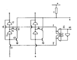
- the invention is explained in more detail with reference to the figure, which shows a schematic circuit diagram of an embodiment of the invention.
- the stages for the first signal 1 and the last signal n of the one-of-n system are shown. These signals are on the corresponding terminals.
- the corresponding signal is connected via the switching path of the first transistor t1 to the input of the first inverter i1 and to the gate of the second transistor t2, the switching path of which lies on the one hand at the circuit zero point and on the other hand via the switching path of the third transistor t3 on all signals 1 ... jointly assigned load element 1 is connected. This is with its other connection to the operating voltage source u.
- Either an enhancement transistor or a depletion transistor of the same channel line type as the transistors mentioned serves as the load element.
- the output of the first inverter i1 is at the input of the second inverter i2 and via the switching path of the fourth transistor t4 at the gate of the third transistor t3.
- the input of the first inverter i1 is located across the switching path of the fifth transistor t5 at the output of the second inverter i2.
- the interrogation pulse as is fed to the pulse shaper if, which uses it to generate two non-overlapping clock signals f, f.
- the pulse shaper if consists of two NOR gates cross-coupled in the manner shown, one of which is preceded by an inverter.
- the first clock signal f generated by the pulse shaper if lies at the gate of the fourth transistor t4 and that of the fifth transistor t5, while the generated second clock signal f is fed to the gate of the first transistor t1.
- the second clock signal f thus has an L level (the more negative of the two binary signal levels H, L), and thus the first transistor t1 is blocked, so that the inverters i1, i2 receive the signal 1 via the conductive transistor t5 ... n save as it was when the last query pulse was started.
- the second clock signal f assumes an H level and the first clock signal f L level, as a result of which the fourth and the fifth transistor t4, t5 are blocked and the first transistor t1 becomes conductive.
- the current level of the signal 1 ... n reaches the gate of the second transistor t2, while the inverse level of the signal 1 ... n remains stored on the gate of the third transistor t3 at the time of the previous interrogation pulse as.
- the fifth transistor t5 ensures that, outside of the interrogation pulses as, the binary level once stored in the arrangement is retained regardless of the signal change, and this signal change only leads to a change in the signal at the output of the first inverter i1 when an interrogation pulse as is present.
- the invention has the advantage, among other things, that even for a one-out-of-n system with a large number n, it requires only a small amount of semiconductor crystal area, since for each signal of the one-out-of-n-system only the crystal area of two inverters and five further MOS -Transistors is required. The result is a very small «query cell».
- a further advantage of the invention is that the circuit of this interrogation cell can be stored, so that, as indicated in the figure, the stored signal can be tapped at the output of the second inverter 12 for further functions if necessary.
- the five transistors t1 ... t5 and the transistors realizing the two inverters i1, i2 are all of the same channel line type.
Landscapes
- Engineering & Computer Science (AREA)
- Theoretical Computer Science (AREA)
- Physics & Mathematics (AREA)
- Nonlinear Science (AREA)
- Quality & Reliability (AREA)
- General Engineering & Computer Science (AREA)
- General Physics & Mathematics (AREA)
- Logic Circuits (AREA)
- Manipulation Of Pulses (AREA)
Claims (1)
Priority Applications (4)
| Application Number | Priority Date | Filing Date | Title |
|---|---|---|---|
| DE8282101667T DE3274709D1 (en) | 1982-03-04 | 1982-03-04 | Insulated-gate field-effect transistor circuit for a one out of n system |
| EP82101667A EP0088135B1 (fr) | 1982-03-04 | 1982-03-04 | Circuit à transistors à effet de champ, à porte isolée, pour un système un parmi n |
| US06/467,620 US4518872A (en) | 1982-03-04 | 1983-02-17 | MOS Transition detector for plural signal lines using non-overlapping complementary interrogation pulses |
| JP58031915A JPS58194432A (ja) | 1982-03-04 | 1983-03-01 | ワン・アウト・オブnシステム用集積回路 |
Applications Claiming Priority (1)
| Application Number | Priority Date | Filing Date | Title |
|---|---|---|---|
| EP82101667A EP0088135B1 (fr) | 1982-03-04 | 1982-03-04 | Circuit à transistors à effet de champ, à porte isolée, pour un système un parmi n |
Publications (2)
| Publication Number | Publication Date |
|---|---|
| EP0088135A1 EP0088135A1 (fr) | 1983-09-14 |
| EP0088135B1 true EP0088135B1 (fr) | 1986-12-10 |
Family
ID=8188903
Family Applications (1)
| Application Number | Title | Priority Date | Filing Date |
|---|---|---|---|
| EP82101667A Expired EP0088135B1 (fr) | 1982-03-04 | 1982-03-04 | Circuit à transistors à effet de champ, à porte isolée, pour un système un parmi n |
Country Status (4)
| Country | Link |
|---|---|
| US (1) | US4518872A (fr) |
| EP (1) | EP0088135B1 (fr) |
| JP (1) | JPS58194432A (fr) |
| DE (1) | DE3274709D1 (fr) |
Families Citing this family (6)
| Publication number | Priority date | Publication date | Assignee | Title |
|---|---|---|---|---|
| JPS59151523A (ja) * | 1983-02-14 | 1984-08-30 | Toshiba Corp | 遷移検出回路 |
| US4710648A (en) * | 1984-05-09 | 1987-12-01 | Hitachi, Ltd. | Semiconductor including signal processor and transient detector for low temperature operation |
| US4700326A (en) * | 1984-06-04 | 1987-10-13 | Fabricom Corporation | Firmware transitional programmable sequential logic controller |
| US4692635A (en) * | 1986-06-26 | 1987-09-08 | National Semiconductor Corp. | Self-timed logic level transition detector |
| FR2619939B1 (fr) * | 1987-09-01 | 1989-12-08 | Thomson Semiconducteurs | Circuit de detection de transitions d'adresses |
| US5122675A (en) * | 1990-10-12 | 1992-06-16 | Vlsi Technology, Inc. | Digital line lock circuit with noise immunity |
Family Cites Families (10)
| Publication number | Priority date | Publication date | Assignee | Title |
|---|---|---|---|---|
| FR1386494A (fr) * | 1963-12-13 | 1965-01-22 | Compteurs Comp D | Procédé et installation de comptage centralisé |
| US3618082A (en) * | 1969-04-09 | 1971-11-02 | Honeywell Inc | Information retrieval system with a remote station hold circuit to preserve a double change in status |
| US3746882A (en) * | 1971-07-02 | 1973-07-17 | North American Rockwell | Input synchronizer circuit |
| US3732407A (en) * | 1971-11-12 | 1973-05-08 | Bell Telephone Labor Inc | Error checked incrementing circuit |
| US3862440A (en) * | 1972-09-14 | 1975-01-21 | Tokyo Shibaura Electric Co | Pulse transforming circuit arrangements using a clock pulse responsive delayed inverter means |
| US4039858A (en) * | 1976-04-05 | 1977-08-02 | Rca Corporation | Transition detector |
| US4176287A (en) * | 1978-04-13 | 1979-11-27 | Motorola, Inc. | Versatile CMOS decoder |
| JPS5597734A (en) * | 1979-01-19 | 1980-07-25 | Toshiba Corp | Logic circuit |
| US4286174A (en) * | 1979-10-01 | 1981-08-25 | Rca Corporation | Transition detector circuit |
| US4420695A (en) * | 1981-05-26 | 1983-12-13 | National Semiconductor Corporation | Synchronous priority circuit |
-
1982
- 1982-03-04 DE DE8282101667T patent/DE3274709D1/de not_active Expired
- 1982-03-04 EP EP82101667A patent/EP0088135B1/fr not_active Expired
-
1983
- 1983-02-17 US US06/467,620 patent/US4518872A/en not_active Expired - Fee Related
- 1983-03-01 JP JP58031915A patent/JPS58194432A/ja active Pending
Also Published As
| Publication number | Publication date |
|---|---|
| JPS58194432A (ja) | 1983-11-12 |
| US4518872A (en) | 1985-05-21 |
| DE3274709D1 (en) | 1987-01-22 |
| EP0088135A1 (fr) | 1983-09-14 |
Similar Documents
| Publication | Publication Date | Title |
|---|---|---|
| DE2723821C2 (de) | Programmierbare logische Anordnung | |
| DE3228013C2 (de) | Bidirektionale Sammelleitung zum Datentransfer | |
| DE68912617T2 (de) | Spannungsseitige MOS-Treiberschaltung. | |
| DE2625007B2 (de) | Adressenpufferschaltung für Halbleiterspeicher | |
| DE2639555A1 (de) | Elektrische integrierte schaltung in einem halbleiterchip | |
| DE3618572A1 (de) | Halbleiterspeicherelement | |
| DE2139170A1 (de) | Binares Addier und Subtrahierwerk | |
| DE2165445C3 (de) | Logikschaltung | |
| EP0088135B1 (fr) | Circuit à transistors à effet de champ, à porte isolée, pour un système un parmi n | |
| DE2165162B2 (de) | CMOS-Halbleiteranordnung als exklusive NOR-Schaltung | |
| DE2422123A1 (de) | Schaltverzoegerungsfreie bistabile schaltung | |
| DE2165160C2 (de) | CMOS-Schaltung als exklusives ODER-Glied | |
| DE2640731A1 (de) | Dynamische decoderstufe | |
| EP0905892B1 (fr) | Bascule RS avec des entrées de validation | |
| EP0735493A1 (fr) | Circuit d'attaque de bus | |
| DE3435752A1 (de) | Schaltung zur zwischenspeicherung digitaler signale | |
| DE2803811A1 (de) | Schaltung zur anpassung von logik-systemen | |
| DE2824862A1 (de) | Monolithisch integrierte digitale halbleiterschaltung | |
| DE3875549T2 (de) | Schaltung zum vergleichen binaerer signalamplituden. | |
| EP0025104B1 (fr) | Montage pour la génération d'un signal d'initialisation au branchement d'une tension d'alimentation constante et de deux tensions d'horloge | |
| EP0333884A1 (fr) | Circuit multiplieur parallèle-série ainsi que ses étages de multiplication et d'addition | |
| EP0093899A1 (fr) | Circuit pour l'adaptation d'un dispositif d'essai à un objet à l'essai | |
| DE19640802C1 (de) | Vorrichtung zur Frequenzteilung mit nicht ganzzahligem Teilungsfaktor | |
| DE2052519B2 (de) | Logische Schaltung | |
| EP0067464B1 (fr) | Compteur binaire synchronisé dynamique à structure identique des étages |
Legal Events
| Date | Code | Title | Description |
|---|---|---|---|
| PUAI | Public reference made under article 153(3) epc to a published international application that has entered the european phase |
Free format text: ORIGINAL CODE: 0009012 |
|
| AK | Designated contracting states |
Designated state(s): DE FR GB IT NL |
|
| 17P | Request for examination filed |
Effective date: 19840204 |
|
| GRAA | (expected) grant |
Free format text: ORIGINAL CODE: 0009210 |
|
| AK | Designated contracting states |
Kind code of ref document: B1 Designated state(s): DE FR GB IT NL |
|
| PG25 | Lapsed in a contracting state [announced via postgrant information from national office to epo] |
Ref country code: IT Free format text: LAPSE BECAUSE OF FAILURE TO SUBMIT A TRANSLATION OF THE DESCRIPTION OR TO PAY THE FEE WITHIN THE PRESCRIBED TIME-LIMIT;WARNING: LAPSES OF ITALIAN PATENTS WITH EFFECTIVE DATE BEFORE 2007 MAY HAVE OCCURRED AT ANY TIME BEFORE 2007. THE CORRECT EFFECTIVE DATE MAY BE DIFFERENT FROM THE ONE RECORDED. Effective date: 19861210 |
|
| REF | Corresponds to: |
Ref document number: 3274709 Country of ref document: DE Date of ref document: 19870122 |
|
| ET | Fr: translation filed | ||
| PG25 | Lapsed in a contracting state [announced via postgrant information from national office to epo] |
Ref country code: NL Effective date: 19871001 |
|
| PLBE | No opposition filed within time limit |
Free format text: ORIGINAL CODE: 0009261 |
|
| STAA | Information on the status of an ep patent application or granted ep patent |
Free format text: STATUS: NO OPPOSITION FILED WITHIN TIME LIMIT |
|
| NLV4 | Nl: lapsed or anulled due to non-payment of the annual fee | ||
| 26N | No opposition filed | ||
| PG25 | Lapsed in a contracting state [announced via postgrant information from national office to epo] |
Ref country code: DE Effective date: 19871201 |
|
| PG25 | Lapsed in a contracting state [announced via postgrant information from national office to epo] |
Ref country code: GB Free format text: LAPSE BECAUSE OF NON-PAYMENT OF DUE FEES Effective date: 19881122 |
|
| GBPC | Gb: european patent ceased through non-payment of renewal fee | ||
| PG25 | Lapsed in a contracting state [announced via postgrant information from national office to epo] |
Ref country code: FR Free format text: LAPSE BECAUSE OF NON-PAYMENT OF DUE FEES Effective date: 19881130 |
|
| REG | Reference to a national code |
Ref country code: FR Ref legal event code: ST |