EP0092442B1 - Circuit de synchronisation de phase - Google Patents
Circuit de synchronisation de phase Download PDFInfo
- Publication number
- EP0092442B1 EP0092442B1 EP83302255A EP83302255A EP0092442B1 EP 0092442 B1 EP0092442 B1 EP 0092442B1 EP 83302255 A EP83302255 A EP 83302255A EP 83302255 A EP83302255 A EP 83302255A EP 0092442 B1 EP0092442 B1 EP 0092442B1
- Authority
- EP
- European Patent Office
- Prior art keywords
- phase
- synchronizing circuit
- frequency
- output
- phase synchronizing
- Prior art date
- Legal status (The legal status is an assumption and is not a legal conclusion. Google has not performed a legal analysis and makes no representation as to the accuracy of the status listed.)
- Expired
Links
- 230000001360 synchronised effect Effects 0.000 claims description 3
- 230000000903 blocking effect Effects 0.000 claims 2
- 238000010586 diagram Methods 0.000 description 4
- 238000010276 construction Methods 0.000 description 3
- 230000010355 oscillation Effects 0.000 description 3
- 230000006866 deterioration Effects 0.000 description 2
- 230000003111 delayed effect Effects 0.000 description 1
- 238000009499 grossing Methods 0.000 description 1
- 238000000034 method Methods 0.000 description 1
- 230000010363 phase shift Effects 0.000 description 1
Images

Classifications
-
- H—ELECTRICITY
- H04—ELECTRIC COMMUNICATION TECHNIQUE
- H04L—TRANSMISSION OF DIGITAL INFORMATION, e.g. TELEGRAPHIC COMMUNICATION
- H04L27/00—Modulated-carrier systems
- H04L27/18—Phase-modulated carrier systems, i.e. using phase-shift keying
- H04L27/22—Demodulator circuits; Receiver circuits
- H04L27/227—Demodulator circuits; Receiver circuits using coherent demodulation
- H04L27/2271—Demodulator circuits; Receiver circuits using coherent demodulation wherein the carrier recovery circuit uses only the demodulated signals
- H04L27/2272—Demodulator circuits; Receiver circuits using coherent demodulation wherein the carrier recovery circuit uses only the demodulated signals using phase locked loops
-
- H—ELECTRICITY
- H03—ELECTRONIC CIRCUITRY
- H03L—AUTOMATIC CONTROL, STARTING, SYNCHRONISATION OR STABILISATION OF GENERATORS OF ELECTRONIC OSCILLATIONS OR PULSES
- H03L7/00—Automatic control of frequency or phase; Synchronisation
- H03L7/06—Automatic control of frequency or phase; Synchronisation using a reference signal applied to a frequency- or phase-locked loop
- H03L7/08—Details of the phase-locked loop
- H03L7/10—Details of the phase-locked loop for assuring initial synchronisation or for broadening the capture range
- H03L7/113—Details of the phase-locked loop for assuring initial synchronisation or for broadening the capture range using frequency discriminator
Definitions
- the present invention relates to a phase synchronizing circuit including a phaselock loop for use in communication systems.
- Phaselock loops find extensive applications to, for example, synchronizing circuits, frequency demodulators, PSK demodulators, frequency synthesizers, etc.
- a phase comparator compares the phase of an input signal with that of an output signal and a loop filter smoothes the comparison output from the comparator to control a voltage controlled oscillator (VCO) whose output constitutes the output signal mentioned above.
- VCO voltage controlled oscillator
- phaselock loop must often be aided by additional pull-in means as typified by frequency sweep. Furthermore, difficulty has been experienced in adopting the phaselock loop when fast pull-in operation is required for a burst operation, as is the case with a PSK demodulator in a time division multiplex access (TDMA) communication system.
- TDMA time division multiplex access
- a frequency synchronizing circuit which includes a PLL incorporating a multiplier, a low pass filter, a voltage adder and a dc amplifier.
- the phase synchronizing circuit of the present invention has an extended pull-in range and a fast pull-in operation.
- a feature of the particular embodiment to be described which contributes to these characteristics and which is not found in previous proposals is a mixer, which constitutes a part of an APC circuit, and which operates at an entry frequency.
- the mixer modulates an input signal with an LF signal to provide a modulated signal.
- the AFC and APC circuits thus operate in mutually different frequency bands, and enable the PLL to operate more effectively upon synchronization.
- a circuit including a phase shifter, mixers and a low pass filter is provided at a stage preceding the basic PLL circuit.
- a phase synchronizing circuit which has a voltage controlled oscillator for generating an output signal in response to a control voltage, a phase comparator for phase-comparing the output signal from the voltage controlled oscillator with a first signal to provide a second signal, and a loop filter for smoothing the second signal to provide the control voltage.
- a phase shifter phase-shifts the output signal by (nI2)+n ⁇ (n being an integer) to provide a third signal with an input signal to provide a fourth signal.
- a low-pass filter selects a low frequency component out of the fourth signal and provides a fifth signal whose phase is delayed in correspondence with the frequency difference between the input and output signals.
- a second mixer is for mixing the fifth signal with the input signal to provide the first signal.
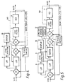
- the basic phaselock loop 100 comprises a voltage controlled oscillator (VCO), a phase comparator 2 and a loop filter 3.
- the phase comparator 2 comprises a mixer or multiplier as is often the case.
- the loop filter 3, on the other hand, comprises a low-pass filter.
- the phase comparator 2 compares the frequency and phase of an input signal V I (t) with those of the output signal Volt) from the VCO 1, generating an average d.c. voltage which is proportional to the difference or error therebetween.
- the error voltage passed through the loop filter 3 is applied to a control terminal of the VCO 1, whereby the frequency of the VCO 1 is varied in a direction that will reduce difference in frequency and phase between the input signal V,(t) and the output signal V o (t). Should the input signal V i (t) entering the phase comparator 2 have a frequency which is sufficiently close to the free oscillation frequency f o of the VCO 1, it would pull in the output of the VCO 1.
- phaselock loop For further details of a phaselock loop, reference is made to F. M. Gardner "Phaselock Techniques", John Wiley & Sons, and other books. Thus, the basic phaselock loop is limited in the available pull-in frequency range.
- phase synchronizing circuit in accordance with the present invention is illustrated, in which the same reference numerals as those of Figure 1 designate the same circuit components.
- the phase synchronizing circuit comprises a ⁇ /2 phase shifter 4, a mixer or multiplier 5, a low-pass filter (LPF) 6 and a second mixer or multiplier 7, in addition to the basic phaselock loop 100 ( Figure 1).
- LPF low-pass filter
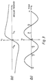
- the input signal V I (t) to the loop and the output signal V o (t) from the loop are respectively assumed to be: where ⁇ i and 8 are the angular frqeuency and phase of the input signal respectively, and ⁇ o and ⁇ o are the oscillation angular frequency and phase of the VCO 1 under zero input condition respectively. Then, the output V 4 (t) of the n/2 phase shifter 4 is produced by:
- the low-pass filter 6 passes only a low frequency component therethrough out of the output of the mixer 5.
- the output V 7 (t) of the mixer 7 is obtained as:
- the phase comparator 2 multiplies or mixes the voltage V 7 (t) by the voltage V o (t), generating an output V 2 (t):
- the second item represents the frequency discrimination characteristic. So long as the absolute value
- ⁇ e enters the synchronizing range, synchronization is rapidly achieved setting up the equation Me 0.
- the phase comparator 2 brings the loop into the phase synchronizing control state.
- the phaselock loop of the present invention functions as an automatic frequency control (AFC) circuit in the unsynchronized state thereby reducing the frequency error, while functioning as a phase synchronizing circuit once the frequency error enters the synchronizing range.
- AFC automatic frequency control
- phase shifter has been shown and described as comprising a ⁇ /2 phase shifter, it will be apparent to those skilled in this art that use may be made of a phase shifter which generally shifts the phase by (n/2)+nn (n being an integer).
- phase synchronizing circuit of Fig. 4 further includes a low-pass filter 6' having a variable time constant, a low-pass filter 8, a level detector (for example, a voltage comparator) 9, and a display 10 such as a light emitting diode.
- the low-pass filter 8 has a band which is narrow enough to suppress input noise.
- the detector 9 detects an output of the low-pass filter 8 with respect to a predetermined reference level.
- the detector 9 when the phaselock loop is being synchronizing, causes the display 10 to indicate the synchronized state. Simultaneously, the detector 9 changes the time constant of the low-pass filter 6' to a larger one. On the other hand, the detector 9, responsive to asynchronization of the phaselock loop, changes the time constant to a smaller one. This switchover of the time constant ensures a wider frequency control range in the unsynchronized state while suppressing the deterioration of the S/N ratio at the multiplier 7 in the synchronized state.
- phase synchronizing circuit of the present invention is shown in Figure 5, in which the same reference numerals as those of Figure 2 or 4 designate the elements common in function.
- the detector 9 upon synchronization, actuates the switch 11 to supply the output voltage of the generator circuit 12 to the mixer 7 and to block the output of the filter 6. Because the output of the low-pass filter 6 is blocked in the above condition reducing the multiplier 7 to a simple pass element, the same operation as in the prior art phaselock loop shown in Figure 1 occurs under the normal condition.
- the mixer 7, therefore, becomes entirely free from the S/N ratio deterioration.
- the present invention overcomes the problem observed in the prior art phaselock loop in the event of pull-in. That is, even when the initial frequency error lies outside the pull-in frequency range of a phaselock loop, the present invetion can serve as a frequency control circuit due to its phase discriminating function; phase synchronization is set up as soon as the frequency error is brought into the synchronizing range.
- the phaselock loop of the present invention is applicable to a PSK demodulator of a TDMA apparatus or the like which has experienced difficulty in adopting the prior art phaselock loop.
Landscapes
- Engineering & Computer Science (AREA)
- Computer Networks & Wireless Communication (AREA)
- Signal Processing (AREA)
- Stabilization Of Oscillater, Synchronisation, Frequency Synthesizers (AREA)
- Superheterodyne Receivers (AREA)
Claims (6)
Applications Claiming Priority (2)
| Application Number | Priority Date | Filing Date | Title |
|---|---|---|---|
| JP64623/82 | 1982-04-20 | ||
| JP57064623A JPS58182323A (ja) | 1982-04-20 | 1982-04-20 | 位相同期回路 |
Publications (3)
| Publication Number | Publication Date |
|---|---|
| EP0092442A2 EP0092442A2 (fr) | 1983-10-26 |
| EP0092442A3 EP0092442A3 (en) | 1985-02-20 |
| EP0092442B1 true EP0092442B1 (fr) | 1988-07-20 |
Family
ID=13263566
Family Applications (1)
| Application Number | Title | Priority Date | Filing Date |
|---|---|---|---|
| EP83302255A Expired EP0092442B1 (fr) | 1982-04-20 | 1983-04-20 | Circuit de synchronisation de phase |
Country Status (5)
| Country | Link |
|---|---|
| US (1) | US4654864A (fr) |
| EP (1) | EP0092442B1 (fr) |
| JP (1) | JPS58182323A (fr) |
| CA (1) | CA1198181A (fr) |
| DE (1) | DE3377444D1 (fr) |
Families Citing this family (12)
| Publication number | Priority date | Publication date | Assignee | Title |
|---|---|---|---|---|
| JPH0732391B2 (ja) * | 1985-05-28 | 1995-04-10 | 日本電気株式会社 | クロック同期回路 |
| US4789948A (en) * | 1985-09-13 | 1988-12-06 | Hughes Aircraft Company | Method and apparatus for determining communications link quality and receiver tracking performance |
| US4799984A (en) * | 1987-09-18 | 1989-01-24 | E. I. Du Pont De Nemours And Company | Method for fabricating multilayer circuits |
| FR2627645A1 (fr) * | 1988-02-18 | 1989-08-25 | Schlumberger Ind Sa | Oscillateur, en particulier a ondes acoustiques de surface, asservi en frequence par commande de sa temperature |
| JPH0719504B2 (ja) * | 1988-11-08 | 1995-03-06 | 三菱電機株式会社 | 断路器 |
| US5097219A (en) * | 1988-12-15 | 1992-03-17 | Mitsubishi Denki Kabushiki Kaisha | Pll for controlling frequency deviation of a variable frequency oscillator |
| US5126998A (en) * | 1990-05-16 | 1992-06-30 | U.V. Satellite Resources, Inc. | Method and apparatus for transmitting and receiving a carrier signal which is simultaneously frequency and phase modulated |
| US5666322A (en) * | 1995-09-21 | 1997-09-09 | Nec Electronics, Inc. | Phase-locked loop timing controller in an integrated circuit memory |
| KR100207656B1 (ko) * | 1996-02-08 | 1999-07-15 | 윤종용 | 디지털 위상 보정 장치 |
| DE19710520C1 (de) | 1997-03-14 | 1998-09-17 | Roland Man Druckmasch | Druckmaschine mit einer Bebilderungsvorrichtung |
| US7873133B2 (en) * | 2005-06-30 | 2011-01-18 | Infinera Corporation | Recovery of client clock without jitter |
| US9407357B1 (en) | 2009-05-29 | 2016-08-02 | Rockwell Collins, Inc. | Systems and methods for radio node synchronization based on range calculations |
Family Cites Families (10)
| Publication number | Priority date | Publication date | Assignee | Title |
|---|---|---|---|---|
| GB1425572A (en) * | 1972-03-14 | 1976-02-18 | Post Office | Digital signal regenerators |
| US3883806A (en) * | 1974-03-07 | 1975-05-13 | Rockwell International Corp | Demodulator circuit for phase modulated communication signals |
| US3906376A (en) * | 1974-06-03 | 1975-09-16 | Rockwell International Corp | Synchronous differentially coherent PSK demodulation |
| CA1063719A (fr) * | 1975-04-28 | 1979-10-02 | Control Data Corporation | Decodeur a boucle d'asservissement de phase |
| US4017803A (en) * | 1976-01-29 | 1977-04-12 | Sperry Rand Corporation | Data recovery system resistant to frequency deviations |
| US4072909A (en) * | 1976-09-27 | 1978-02-07 | Zenith Radio Corporation | Automatic phase and frequency control system |
| JPS56129432A (en) * | 1980-03-14 | 1981-10-09 | Nec Corp | Frequency synchronizing circuit |
| US4347483A (en) * | 1980-07-28 | 1982-08-31 | Zenith Radio Corporation | Frequency and phase lock loop with separated AFC and phase locking |
| US4387342A (en) * | 1981-03-04 | 1983-06-07 | Datavision, Inc. | Phase-shift keyed decoder |
| US4419760A (en) * | 1982-01-29 | 1983-12-06 | Motorola Inc. | Augmented phase-locked loop for very wide range acquisition and method therefor |
-
1982
- 1982-04-20 JP JP57064623A patent/JPS58182323A/ja active Pending
-
1983
- 1983-04-19 US US06/486,576 patent/US4654864A/en not_active Expired - Fee Related
- 1983-04-19 CA CA000426153A patent/CA1198181A/fr not_active Expired
- 1983-04-20 DE DE8383302255T patent/DE3377444D1/de not_active Expired
- 1983-04-20 EP EP83302255A patent/EP0092442B1/fr not_active Expired
Also Published As
| Publication number | Publication date |
|---|---|
| CA1198181A (fr) | 1985-12-17 |
| DE3377444D1 (en) | 1988-08-25 |
| EP0092442A3 (en) | 1985-02-20 |
| US4654864A (en) | 1987-03-31 |
| EP0092442A2 (fr) | 1983-10-26 |
| JPS58182323A (ja) | 1983-10-25 |
Similar Documents
| Publication | Publication Date | Title |
|---|---|---|
| EP0644657B1 (fr) | Circuit de boucle à verrouillage de phase | |
| US5563921A (en) | Jitter detection apparatus using double-PLL structure | |
| EP0445522B1 (fr) | Méthode de capture d'émissions par satellite pour récepteur GPS | |
| US5737694A (en) | Highly stable frequency synthesizer loop with feedforward | |
| EP0092442B1 (fr) | Circuit de synchronisation de phase | |
| US4072905A (en) | Wide acquisition range MSK demodulator input circuit | |
| US4339725A (en) | Synchronous demodulator for multi-phase PSK signal | |
| US4628270A (en) | Frequency-agile synchronous demodulator | |
| EP0557867B1 (fr) | Circuit à double boucle à verrouillage de phase | |
| US5296820A (en) | Coherent demodulator preceded by non-coherent demodulator and automatic frequency control circuit | |
| US4461035A (en) | Television synchronous receiver | |
| EP0176703B1 (fr) | Unité de traitement de signaux de fréquence intermédiaire | |
| US4163951A (en) | Frequency discriminator producing at least one of two pulse sequences representing in average the result of frequency discrimination | |
| EP0771076A1 (fr) | Synthétiseur de fréquence | |
| KR100261805B1 (ko) | 원하는위상에주파수및위상로킹회로를로킹시키기위한회로 | |
| US7050520B2 (en) | PLL (Phase-Locked Loop) circuit | |
| WO1991007016A1 (fr) | Boucle a verrouillage de phase servant a produire une porteuse de reference pour un detecteur coherent | |
| JP3254009B2 (ja) | 位相固定ループを含む回路 | |
| US6628345B1 (en) | Automatic frequency tuning circuit | |
| JP3462277B2 (ja) | 搬送波再生回路 | |
| CA2234855C (fr) | Boucle synthetiseur de frequences hautement stable a precompensation | |
| JPH03212024A (ja) | 周波数シンセサイザ | |
| JPH04268820A (ja) | フェイズロックループ | |
| JPS609204A (ja) | テレビジヨン信号の検波回路 | |
| GB2160037A (en) | Phase locked loop circuits |
Legal Events
| Date | Code | Title | Description |
|---|---|---|---|
| PUAI | Public reference made under article 153(3) epc to a published international application that has entered the european phase |
Free format text: ORIGINAL CODE: 0009012 |
|
| AK | Designated contracting states |
Designated state(s): DE FR GB IT |
|
| PUAL | Search report despatched |
Free format text: ORIGINAL CODE: 0009013 |
|
| AK | Designated contracting states |
Designated state(s): DE FR GB IT |
|
| 17P | Request for examination filed |
Effective date: 19850222 |
|
| 17Q | First examination report despatched |
Effective date: 19860217 |
|
| R17C | First examination report despatched (corrected) |
Effective date: 19870625 |
|
| GRAA | (expected) grant |
Free format text: ORIGINAL CODE: 0009210 |
|
| AK | Designated contracting states |
Kind code of ref document: B1 Designated state(s): DE FR GB IT |
|
| REF | Corresponds to: |
Ref document number: 3377444 Country of ref document: DE Date of ref document: 19880825 |
|
| ITF | It: translation for a ep patent filed | ||
| ET | Fr: translation filed | ||
| PLBE | No opposition filed within time limit |
Free format text: ORIGINAL CODE: 0009261 |
|
| STAA | Information on the status of an ep patent application or granted ep patent |
Free format text: STATUS: NO OPPOSITION FILED WITHIN TIME LIMIT |
|
| 26N | No opposition filed | ||
| ITTA | It: last paid annual fee | ||
| PGFP | Annual fee paid to national office [announced via postgrant information from national office to epo] |
Ref country code: FR Payment date: 19990409 Year of fee payment: 17 |
|
| PGFP | Annual fee paid to national office [announced via postgrant information from national office to epo] |
Ref country code: GB Payment date: 19990421 Year of fee payment: 17 |
|
| PGFP | Annual fee paid to national office [announced via postgrant information from national office to epo] |
Ref country code: DE Payment date: 19990426 Year of fee payment: 17 |
|
| PG25 | Lapsed in a contracting state [announced via postgrant information from national office to epo] |
Ref country code: GB Free format text: LAPSE BECAUSE OF NON-PAYMENT OF DUE FEES Effective date: 20000420 |
|
| GBPC | Gb: european patent ceased through non-payment of renewal fee |
Effective date: 20000420 |
|
| PG25 | Lapsed in a contracting state [announced via postgrant information from national office to epo] |
Ref country code: FR Free format text: LAPSE BECAUSE OF NON-PAYMENT OF DUE FEES Effective date: 20001229 |
|
| PG25 | Lapsed in a contracting state [announced via postgrant information from national office to epo] |
Ref country code: DE Free format text: LAPSE BECAUSE OF NON-PAYMENT OF DUE FEES Effective date: 20010201 |
|
| REG | Reference to a national code |
Ref country code: FR Ref legal event code: ST |