EP0110103B1 - Verfahren zum Herstellen einer CMOS-Struktur - Google Patents
Verfahren zum Herstellen einer CMOS-Struktur Download PDFInfo
- Publication number
- EP0110103B1 EP0110103B1 EP83110499A EP83110499A EP0110103B1 EP 0110103 B1 EP0110103 B1 EP 0110103B1 EP 83110499 A EP83110499 A EP 83110499A EP 83110499 A EP83110499 A EP 83110499A EP 0110103 B1 EP0110103 B1 EP 0110103B1
- Authority
- EP
- European Patent Office
- Prior art keywords
- forming
- source
- type
- region
- metal oxide
- Prior art date
- Legal status (The legal status is an assumption and is not a legal conclusion. Google has not performed a legal analysis and makes no representation as to the accuracy of the status listed.)
- Expired
Links
- 239000004065 semiconductor Substances 0.000 title claims description 22
- 230000000295 complement effect Effects 0.000 title claims description 15
- 229910044991 metal oxide Inorganic materials 0.000 title claims description 12
- 150000004706 metal oxides Chemical class 0.000 title claims description 12
- 238000004519 manufacturing process Methods 0.000 title description 5
- 238000000034 method Methods 0.000 claims description 43
- 239000000758 substrate Substances 0.000 claims description 19
- 230000003647 oxidation Effects 0.000 claims description 17
- 238000007254 oxidation reaction Methods 0.000 claims description 17
- 229920002120 photoresistant polymer Polymers 0.000 claims description 14
- 230000004888 barrier function Effects 0.000 claims description 12
- 239000012535 impurity Substances 0.000 claims description 12
- 238000002955 isolation Methods 0.000 claims description 11
- 238000002161 passivation Methods 0.000 claims description 7
- 229910052796 boron Inorganic materials 0.000 claims description 5
- ZOXJGFHDIHLPTG-UHFFFAOYSA-N Boron Chemical group [B] ZOXJGFHDIHLPTG-UHFFFAOYSA-N 0.000 claims description 3
- 229910052785 arsenic Inorganic materials 0.000 claims description 2
- RQNWIZPPADIBDY-UHFFFAOYSA-N arsenic atom Chemical group [As] RQNWIZPPADIBDY-UHFFFAOYSA-N 0.000 claims description 2
- 230000015572 biosynthetic process Effects 0.000 claims description 2
- 230000001590 oxidative effect Effects 0.000 claims 1
- 229910052698 phosphorus Inorganic materials 0.000 description 10
- VYPSYNLAJGMNEJ-UHFFFAOYSA-N Silicium dioxide Chemical compound O=[Si]=O VYPSYNLAJGMNEJ-UHFFFAOYSA-N 0.000 description 8
- 229910052757 nitrogen Inorganic materials 0.000 description 8
- 229910052581 Si3N4 Inorganic materials 0.000 description 7
- 239000004020 conductor Substances 0.000 description 7
- HQVNEWCFYHHQES-UHFFFAOYSA-N silicon nitride Chemical compound N12[Si]34N5[Si]62N3[Si]51N64 HQVNEWCFYHHQES-UHFFFAOYSA-N 0.000 description 7
- 238000009792 diffusion process Methods 0.000 description 6
- 239000007943 implant Substances 0.000 description 4
- 239000012212 insulator Substances 0.000 description 4
- 235000012239 silicon dioxide Nutrition 0.000 description 4
- 239000000377 silicon dioxide Substances 0.000 description 4
- TXEYQDLBPFQVAA-UHFFFAOYSA-N tetrafluoromethane Chemical compound FC(F)(F)F TXEYQDLBPFQVAA-UHFFFAOYSA-N 0.000 description 4
- ZXEYZECDXFPJRJ-UHFFFAOYSA-N $l^{3}-silane;platinum Chemical compound [SiH3].[Pt] ZXEYZECDXFPJRJ-UHFFFAOYSA-N 0.000 description 3
- XUIMIQQOPSSXEZ-UHFFFAOYSA-N Silicon Chemical compound [Si] XUIMIQQOPSSXEZ-UHFFFAOYSA-N 0.000 description 3
- 229910052782 aluminium Inorganic materials 0.000 description 3
- XAGFODPZIPBFFR-UHFFFAOYSA-N aluminium Chemical compound [Al] XAGFODPZIPBFFR-UHFFFAOYSA-N 0.000 description 3
- 239000002019 doping agent Substances 0.000 description 3
- 238000005468 ion implantation Methods 0.000 description 3
- 150000002500 ions Chemical class 0.000 description 3
- 229910021339 platinum silicide Inorganic materials 0.000 description 3
- 229910052710 silicon Inorganic materials 0.000 description 3
- 239000010703 silicon Substances 0.000 description 3
- QVGXLLKOCUKJST-UHFFFAOYSA-N atomic oxygen Chemical compound [O] QVGXLLKOCUKJST-UHFFFAOYSA-N 0.000 description 2
- -1 boron ions Chemical class 0.000 description 2
- 238000005530 etching Methods 0.000 description 2
- 238000010438 heat treatment Methods 0.000 description 2
- 229910052760 oxygen Inorganic materials 0.000 description 2
- 239000001301 oxygen Substances 0.000 description 2
- MYMOFIZGZYHOMD-UHFFFAOYSA-N Dioxygen Chemical compound O=O MYMOFIZGZYHOMD-UHFFFAOYSA-N 0.000 description 1
- VEXZGXHMUGYJMC-UHFFFAOYSA-N Hydrochloric acid Chemical compound Cl VEXZGXHMUGYJMC-UHFFFAOYSA-N 0.000 description 1
- UFHFLCQGNIYNRP-UHFFFAOYSA-N Hydrogen Chemical compound [H][H] UFHFLCQGNIYNRP-UHFFFAOYSA-N 0.000 description 1
- 230000004913 activation Effects 0.000 description 1
- 238000000137 annealing Methods 0.000 description 1
- HAYXDMNJJFVXCI-UHFFFAOYSA-N arsenic(5+) Chemical compound [As+5] HAYXDMNJJFVXCI-UHFFFAOYSA-N 0.000 description 1
- 238000000151 deposition Methods 0.000 description 1
- 229910001882 dioxygen Inorganic materials 0.000 description 1
- 230000009977 dual effect Effects 0.000 description 1
- 239000007772 electrode material Substances 0.000 description 1
- 230000005669 field effect Effects 0.000 description 1
- 239000007789 gas Substances 0.000 description 1
- 229910000041 hydrogen chloride Inorganic materials 0.000 description 1
- IXCSERBJSXMMFS-UHFFFAOYSA-N hydrogen chloride Substances Cl.Cl IXCSERBJSXMMFS-UHFFFAOYSA-N 0.000 description 1
- 238000004518 low pressure chemical vapour deposition Methods 0.000 description 1
- 230000000873 masking effect Effects 0.000 description 1
- 239000000463 material Substances 0.000 description 1
- 230000003071 parasitic effect Effects 0.000 description 1
- 229910021420 polycrystalline silicon Inorganic materials 0.000 description 1
- 229920005591 polysilicon Polymers 0.000 description 1
- 230000003068 static effect Effects 0.000 description 1
Images

Classifications
-
- H—ELECTRICITY
- H10—SEMICONDUCTOR DEVICES; ELECTRIC SOLID-STATE DEVICES NOT OTHERWISE PROVIDED FOR
- H10D—INORGANIC ELECTRIC SEMICONDUCTOR DEVICES
- H10D64/00—Electrodes of devices having potential barriers
- H10D64/60—Electrodes characterised by their materials
- H10D64/66—Electrodes having a conductor capacitively coupled to a semiconductor by an insulator, e.g. MIS electrodes
- H10D64/665—Electrodes having a conductor capacitively coupled to a semiconductor by an insulator, e.g. MIS electrodes the conductor comprising a layer of elemental metal contacting the insulator, e.g. tungsten or molybdenum
-
- H—ELECTRICITY
- H10—SEMICONDUCTOR DEVICES; ELECTRIC SOLID-STATE DEVICES NOT OTHERWISE PROVIDED FOR
- H10D—INORGANIC ELECTRIC SEMICONDUCTOR DEVICES
- H10D62/00—Semiconductor bodies, or regions thereof, of devices having potential barriers
- H10D62/10—Shapes, relative sizes or dispositions of the regions of the semiconductor bodies; Shapes of the semiconductor bodies
- H10D62/102—Constructional design considerations for preventing surface leakage or controlling electric field concentration
- H10D62/112—Constructional design considerations for preventing surface leakage or controlling electric field concentration for preventing surface leakage due to surface inversion layers, e.g. by using channel stoppers
-
- H—ELECTRICITY
- H10—SEMICONDUCTOR DEVICES; ELECTRIC SOLID-STATE DEVICES NOT OTHERWISE PROVIDED FOR
- H10D—INORGANIC ELECTRIC SEMICONDUCTOR DEVICES
- H10D64/00—Electrodes of devices having potential barriers
- H10D64/60—Electrodes characterised by their materials
- H10D64/66—Electrodes having a conductor capacitively coupled to a semiconductor by an insulator, e.g. MIS electrodes
- H10D64/667—Electrodes having a conductor capacitively coupled to a semiconductor by an insulator, e.g. MIS electrodes the conductor comprising a layer of alloy material, compound material or organic material contacting the insulator, e.g. TiN workfunction layers
- H10D64/668—Electrodes having a conductor capacitively coupled to a semiconductor by an insulator, e.g. MIS electrodes the conductor comprising a layer of alloy material, compound material or organic material contacting the insulator, e.g. TiN workfunction layers the layer being a silicide, e.g. TiSi2
-
- H—ELECTRICITY
- H10—SEMICONDUCTOR DEVICES; ELECTRIC SOLID-STATE DEVICES NOT OTHERWISE PROVIDED FOR
- H10D—INORGANIC ELECTRIC SEMICONDUCTOR DEVICES
- H10D84/00—Integrated devices formed in or on semiconductor substrates that comprise only semiconducting layers, e.g. on Si wafers or on GaAs-on-Si wafers
- H10D84/01—Manufacture or treatment
- H10D84/0123—Integrating together multiple components covered by H10D12/00 or H10D30/00, e.g. integrating multiple IGBTs
- H10D84/0126—Integrating together multiple components covered by H10D12/00 or H10D30/00, e.g. integrating multiple IGBTs the components including insulated gates, e.g. IGFETs
- H10D84/0165—Integrating together multiple components covered by H10D12/00 or H10D30/00, e.g. integrating multiple IGBTs the components including insulated gates, e.g. IGFETs the components including complementary IGFETs, e.g. CMOS devices
- H10D84/017—Manufacturing their source or drain regions, e.g. silicided source or drain regions
-
- H—ELECTRICITY
- H10—SEMICONDUCTOR DEVICES; ELECTRIC SOLID-STATE DEVICES NOT OTHERWISE PROVIDED FOR
- H10D—INORGANIC ELECTRIC SEMICONDUCTOR DEVICES
- H10D84/00—Integrated devices formed in or on semiconductor substrates that comprise only semiconducting layers, e.g. on Si wafers or on GaAs-on-Si wafers
- H10D84/01—Manufacture or treatment
- H10D84/0123—Integrating together multiple components covered by H10D12/00 or H10D30/00, e.g. integrating multiple IGBTs
- H10D84/0126—Integrating together multiple components covered by H10D12/00 or H10D30/00, e.g. integrating multiple IGBTs the components including insulated gates, e.g. IGFETs
- H10D84/0165—Integrating together multiple components covered by H10D12/00 or H10D30/00, e.g. integrating multiple IGBTs the components including insulated gates, e.g. IGFETs the components including complementary IGFETs, e.g. CMOS devices
- H10D84/0172—Manufacturing their gate conductors
-
- H—ELECTRICITY
- H10—SEMICONDUCTOR DEVICES; ELECTRIC SOLID-STATE DEVICES NOT OTHERWISE PROVIDED FOR
- H10D—INORGANIC ELECTRIC SEMICONDUCTOR DEVICES
- H10D84/00—Integrated devices formed in or on semiconductor substrates that comprise only semiconducting layers, e.g. on Si wafers or on GaAs-on-Si wafers
- H10D84/01—Manufacture or treatment
- H10D84/02—Manufacture or treatment characterised by using material-based technologies
- H10D84/03—Manufacture or treatment characterised by using material-based technologies using Group IV technology, e.g. silicon technology or silicon-carbide [SiC] technology
- H10D84/038—Manufacture or treatment characterised by using material-based technologies using Group IV technology, e.g. silicon technology or silicon-carbide [SiC] technology using silicon technology, e.g. SiGe
Definitions
- This invention relates to a method of making very dense integrated semiconductor structures and, more particularly, to a simple method of making a dense array of transistors in the complementary metal oxide semiconductor (CMOS) technology wherein both N and P channel transistors are formed on a common substrate.
- CMOS complementary metal oxide semiconductor
- CMOS structures are inherently limited by (1) lateral/vertical bipolar parasitic devices leading to latch-up, (2) non-complementary thresholds for the N and P channel devices, (3) difficulty in forming an N well with total compatibility for the N channel device, (4) incorporating a guardring without serious area penalties, (5) tolerance on effective channel length and (6) severe topology.
- CMOS devices Processes for providing CMOS devices are taught in, e.g., US-A-4 002 501 and US-A-4 183 134. These patents teach processes for making complementary devices which have controlled channel lengths and low gate overlap capacitance by the use of thick insulators over their source and drain regions.
- the method includes applying a photoresist layer over the insulating layer with an opening over one of the thin insulating films, introducing a first impurity into the channel region of the one portion to adjust the impurity therein, depositing a first conductive material on the thin insulating film located over the channel region of the one portion.
- the photoresist layer is then removed and a second impurity is introduced into the channel region of the other portion to adjust the impurity therein.
- a second conductive material is deposited on the thin insulating film located over the channel region of the other portion and in contact with the first conductive material, with the second conductive material having a different work function than that of the first conductive material.
- the first conductive material is, preferably, platinum silicide while the second conductive material may be aluminum.
- the invention as claimed is intended to provide a process for making a very planar CMOS structure, particularly a bulk structure, to achieve high density and better overall control of parameters with minimal dopant diffusions for optimal device profile control.
- a process for making a planar CMOS structure having work function-adjusted N and P devices wherein the gate insulator is formed initially and then no appreciable thermal process steps are provided until at the end of the process when a single oxidation provides isolation and source-drain passivation concurrently after the P or N well, P channel and N channel source/drain regions, and field threshold adjust implant are in place. Also, the field dopant for the N channel device is introduced after the gate dielectric layer, source/drain diffusions and the P well are substantially fabricated.
- CMOS complementary metal oxide semiconductor
- a process for making a complementary metal oxide semiconductor (CMOS) bulk structure which includes forming an oxidation barrier layer on a semiconductor substrate of a given conductivity type having first and second portions.
- a well is formed in the first portion of the substrate having a conductivity of opposite type to that of the given conductivity type.
- Source and drain regions are then defined in the well and a first channel region therebetween.
- a first portion of the oxidation barrier layer over the source and drain regions is removed and a first impurity of the given conductivity type is implanted into the source and drain regions.
- a thermal step may be employed to essentially form the final diffusion profile.
- a field region in the well is defined and a second portion of the oxidation barrier layer over the field region is removed.
- the process then includes implanting a second impurity of the opposite conductivity type into the field region, defining source and drain regions in the second portion of the substrate and a second channel region therebetween, removing a third portion of the oxidation barrier layer over the second portion source and drain regions and implanting a third impurity of the opposite conductivity type into the second portion source and drain regions.
- An isolation region is defined in the substrate outside of the first and second channel regions and a fourth portion of the oxidation barrier layer over the isolation region is removed. The entire surface of the substrate outside of the first and second channel regions is then oxidized.
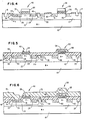
- Fig. 1- a sectional view of the CMOS structure made in accordance with the process of the present invention during an early stage of the fabrication thereof.
- the structure includes a semiconductor substrate 10, which is of an N + conductivity type silicon and an epitaxial semiconductor layer 12, preferably N- type silicon, grown on substrate 10.
- a thin layer of silicon dioxide 14 is grown on the epitaxial layer 12 and a layer of silicon nitride 16 is deposited, preferably by known low pressure chemical vapor deposition techniques, on the silicon dioxide layer 14.
- the thickness of the epitaxial silicon layer 12 may be from 1 to 15 micrometers and have a resistivity range from 5 to 50 ohm-centimeters, and each of the layers 14 and 16 may be 15 nanometers thick.
- openings 18 and 20 are formed in the epitaxial layer 12 to provide alignment marks by etching the silicon nitride and silicon dioxide layers 16 and 14, respectively, in carbon tetrafluoride (CF 4 ) and oxygen gas followed by carbon tetrafluoride and hydrogen gas and by etching about 0.3 micrometers of the epitaxial layer 12 in carbon tetrafluoride and oxygen.
- the photoresist mask is then stripped in an oxygen plasma and the surface of the remaining structure cleaned by any known process.
- a second photoresist mask is provided over the silicon nitride layer 16 to define a P- well 22, wherein boron ions are implanted and driven in partially by a known heat process after the photoresist mask is removed.
- a layer of oxynitride 24 is grown on the silicon nitride layer 16 and an oxide is grown in openings 18 and 20 during this thermal step.
- a third mask is provided to define N++ source and drain regions 26 and 28 in P- well 22 and an N++ contact region 30 in N- epitaxial layer 12 aligned with openings 32, 34 and 36, respectively, in oxynitride layer 24 and silicon nitride layer 16.
- the N++ region 30 spaced from P- well 22 by region 31 may be used to serve as a guardring to limit latch-up. Openings 32 and 34 define the gate dielectric medium 38 for an N channel device 40.
- N++ source and drain regions 26 and 28, respectively, and contact region 30 are then formed by known arsenic ion implantation techniques at an energy of, preferably, 50 KeV with a dose of 4 x 10 15 per square centimeter. If desired, the N++ diffusions may be driven in to virtually their final depth by an inert annealing step. This permits minimal subsequent heat treatments that provide for minimal field encroachment into the active N device channel region and allows minimum depth P channel sources and drains.
- a fourth photoresist mask 42 having openings 44 and 46 therein is provided over the oxynitride layer 24 to define P+ field regions 48 and 50, shown more clearly in Fig. 3 of the drawings.
- the regions 48 and 50 are lightly doped, e.g., 10 11 ions per square centimeter, with preferably boron ions after the oxynitride layer 24 and silicon nitride layer 16 are appropriately removed from the openings 44 and 46. It should be noted that the N channel field regions 48 and 50 are, preferably, fully contained within the P well.
- a fifth mask defines openings 52 and 54, and thus gate dielectric medium 56 for a P channel device 58, and also P++ source and drain regions 60 and 62, indicated in Fig. 3 of the drawings.
- the fifth mask is also provided with an opening 45 over a portion of the field region 50 to form a P well contact region 51.
- P++ source, drain and P well contact ion implants with, preferably, boron, are introduced into the epitaxial layer 12 through the. openings 45, 52 and 54, at an energy of, preferably, 10-50 KeV with a dose of 2-5 x 10 15 per square centimeter or BF 2 at 5-25 KeV and 2-5 x 10 15 per square centimeter.
- a sixth photoresist mask 64 shown in Fig.
- a field isolation and source and drain regions passivation layer 66 illustrated in Fig. 5.
- the exposed oxynitride layer 24 and the silicon nitride layer 16, i.e., all of layers 24 and 16 except in gate dielectric media 38 and 56, are etched away, as indicated in Fig. 4 and then the photoresist mask 64 is removed by known techniques.
- a relatively thick insulating layer 66 serving as field isolation and source-drain region passivation.
- high pressure oxidation could be used, or very low temperature plasma enhanced oxidation, as is known. The latter permits extremely low temperature processing which is desirable for extremely high density device structures.
- the boron and arsenic are driven further into the epitaxial layer 12 or activated to form substantially the final P and N type diffusion regions shown in Fig. 5.
- a seventh photoresist mask is provided having an opening aligned with the gate dielectric layer 56 of the P channel device 58.
- the channel region of the device 58 is threshold adjusted through the opening in the seventh mask and a work function-adjusted electrode material, such as platinum silicide, is evaporated over the gate dielectric layer 56 to form the P channel gate electrode 68.
- a work function-adjusted electrode material such as platinum silicide
- the channel region threshold of the N channel device 40 is adjusted by ion implantation using the gate electrode 68 as a mask for the implanted ions, followed by a short activation anneal.
- a gate electrode 70, or land pattern, preferably made of aluminum, may be formed over the gate dielectric medium 38 for the N channel device 40.
- the method in accordance with the teachings of this invention is very simple, requiring only seven masking steps and provides a very dense bulk CMOS structure.
- the channel lengths of the P channel and N channel transistors are tightly controlled to provide short channels resulting in higher speeds. Since the process provides thick oxides over the sources and drains of the P channel and N channel transistors, the structure has a low gate electrode overlap capacitance. Als, the process provides separate field region controls inside the P well 22 without severe compensation at the edge thereof which permits closer spacing between N++ region 28 and P++ region 60 without encountering a latch-up problem.
- the process of this invention provides a unique bulk CMOS structure, i.e., without the need of a dielectric substrate, which has improved planarity. Furthermore, the process of this invention provides an improved method for obtaining isolation and source/drain passivation simultaneously, i.e., during one process step, with minimal dopant diffusions. It can be seen that in this bulk CMOS process all P or N well, P channel and N channel source/drain regions, gate insulators and field threshold adjust implants are in place before the surface of the epitaxial layer 12 is oxidized for isolation and passivation purposes. Also, the process provides independent N and P region doping in the field region and separate threshold adjustment implants, in view of the predetermined doping levels established during the growth of the N- epitaxial layer 12.
- the epitaxial layer 12 need not be provided in the practice of this invention and that an N- well may be formed in a P substrate or a P or P+ epitaxial layer. Also, dual wells may be provided, i.e., independently doped N and P wells in an intrinsic epitaxial layer.
- platinum silicide and aluminum have been suggested hereinabove for use in making the structure, various other known materials, such as P+ polysilicon and well known polycides, may likewise be used.
- the process and structure of this invention may be conveniently used to make logic circuitry, e.g., a 3-way NOR circuit, or an array of random access memory cells, e.g., static cells.
- logic circuitry e.g., a 3-way NOR circuit
- random access memory cells e.g., static cells.
Landscapes
- Metal-Oxide And Bipolar Metal-Oxide Semiconductor Integrated Circuits (AREA)
Claims (11)
Applications Claiming Priority (2)
| Application Number | Priority Date | Filing Date | Title |
|---|---|---|---|
| US06/446,793 US4462151A (en) | 1982-12-03 | 1982-12-03 | Method of making high density complementary transistors |
| US446793 | 1982-12-03 |
Publications (2)
| Publication Number | Publication Date |
|---|---|
| EP0110103A1 EP0110103A1 (de) | 1984-06-13 |
| EP0110103B1 true EP0110103B1 (de) | 1987-06-16 |
Family
ID=23773851
Family Applications (1)
| Application Number | Title | Priority Date | Filing Date |
|---|---|---|---|
| EP83110499A Expired EP0110103B1 (de) | 1982-12-03 | 1983-10-21 | Verfahren zum Herstellen einer CMOS-Struktur |
Country Status (4)
| Country | Link |
|---|---|
| US (1) | US4462151A (de) |
| EP (1) | EP0110103B1 (de) |
| JP (1) | JPS59106144A (de) |
| DE (1) | DE3372150D1 (de) |
Families Citing this family (12)
| Publication number | Priority date | Publication date | Assignee | Title |
|---|---|---|---|---|
| US4621412A (en) * | 1984-09-17 | 1986-11-11 | Sony Corporation | Manufacturing a complementary MOSFET |
| US4749662A (en) * | 1984-12-14 | 1988-06-07 | Rockwell International Corporation | Diffused field CMOS-bulk process |
| US4675982A (en) * | 1985-10-31 | 1987-06-30 | International Business Machines Corporation | Method of making self-aligned recessed oxide isolation regions |
| JP3271972B2 (ja) * | 1989-03-02 | 2002-04-08 | サンダーバード テクノロジーズ インコーポレイテッド | フェルミしきい値電界効果トランジスタ |
| US5132236A (en) * | 1991-07-30 | 1992-07-21 | Micron Technology, Inc. | Method of semiconductor manufacture using an inverse self-aligned mask |
| EP0562309B1 (de) * | 1992-03-25 | 2002-06-12 | Texas Instruments Incorporated | Planares Verfahren unter Verwendung von gemeinsamen Ausrichtungsmarken für die Wannenimplantierungen |
| TW322629B (en) * | 1996-09-06 | 1997-12-11 | Holtek Microelectronics Inc | Manufacturing method of integrated circuit alignment mark |
| US6686612B1 (en) | 2002-10-01 | 2004-02-03 | T-Ram, Inc. | Thyristor-based device adapted to inhibit parasitic current |
| US6690039B1 (en) | 2002-10-01 | 2004-02-10 | T-Ram, Inc. | Thyristor-based device that inhibits undesirable conductive channel formation |
| US7183221B2 (en) * | 2003-11-06 | 2007-02-27 | Texas Instruments Incorporated | Method of fabricating a semiconductor having dual gate electrodes using a composition-altered metal layer |
| US8373233B2 (en) * | 2008-11-13 | 2013-02-12 | Applied Materials, Inc. | Highly N-type and P-type co-doping silicon for strain silicon application |
| US20240413004A1 (en) * | 2023-06-08 | 2024-12-12 | Nanya Technology Corporation | Semiconductor device manufacturing method for reducing random dopant fluctuation |
Family Cites Families (16)
| Publication number | Priority date | Publication date | Assignee | Title |
|---|---|---|---|---|
| US3700507A (en) * | 1969-10-21 | 1972-10-24 | Rca Corp | Method of making complementary insulated gate field effect transistors |
| US3806371A (en) * | 1971-07-28 | 1974-04-23 | Motorola Inc | Method of making complementary monolithic insulated gate field effect transistors having low threshold voltage and low leakage current |
| US3920481A (en) * | 1974-06-03 | 1975-11-18 | Fairchild Camera Instr Co | Process for fabricating insulated gate field effect transistor structure |
| US4002501A (en) * | 1975-06-16 | 1977-01-11 | Rockwell International Corporation | High speed, high yield CMOS/SOS process |
| US4045250A (en) * | 1975-08-04 | 1977-08-30 | Rca Corporation | Method of making a semiconductor device |
| JPS5286083A (en) * | 1976-01-12 | 1977-07-16 | Hitachi Ltd | Production of complimentary isolation gate field effect transistor |
| JPS5333074A (en) * | 1976-09-08 | 1978-03-28 | Sanyo Electric Co Ltd | Production of complementary type insulated gate field effect semiconductor device |
| US4183134A (en) * | 1977-02-15 | 1980-01-15 | Westinghouse Electric Corp. | High yield processing for silicon-on-sapphire CMOS integrated circuits |
| US4313768A (en) * | 1978-04-06 | 1982-02-02 | Harris Corporation | Method of fabricating improved radiation hardened self-aligned CMOS having Si doped Al field gate |
| JPS5529116A (en) * | 1978-08-23 | 1980-03-01 | Hitachi Ltd | Manufacture of complementary misic |
| JPS56134757A (en) * | 1980-03-26 | 1981-10-21 | Nec Corp | Complementary type mos semiconductor device and its manufacture |
| US4391650A (en) * | 1980-12-22 | 1983-07-05 | Ncr Corporation | Method for fabricating improved complementary metal oxide semiconductor devices |
| NL187328C (nl) * | 1980-12-23 | 1991-08-16 | Philips Nv | Werkwijze ter vervaardiging van een halfgeleiderinrichting. |
| US4385947A (en) * | 1981-07-29 | 1983-05-31 | Harris Corporation | Method for fabricating CMOS in P substrate with single guard ring using local oxidation |
| US4406710A (en) * | 1981-10-15 | 1983-09-27 | Davies Roderick D | Mask-saving technique for forming CMOS source/drain regions |
| US4422885A (en) * | 1981-12-18 | 1983-12-27 | Ncr Corporation | Polysilicon-doped-first CMOS process |
-
1982
- 1982-12-03 US US06/446,793 patent/US4462151A/en not_active Expired - Lifetime
-
1983
- 1983-07-29 JP JP58137951A patent/JPS59106144A/ja active Pending
- 1983-10-21 DE DE8383110499T patent/DE3372150D1/de not_active Expired
- 1983-10-21 EP EP83110499A patent/EP0110103B1/de not_active Expired
Also Published As
| Publication number | Publication date |
|---|---|
| EP0110103A1 (de) | 1984-06-13 |
| US4462151A (en) | 1984-07-31 |
| DE3372150D1 (en) | 1987-07-23 |
| JPS59106144A (ja) | 1984-06-19 |
Similar Documents
| Publication | Publication Date | Title |
|---|---|---|
| US5753556A (en) | Method of fabricating a MIS transistor | |
| US5783469A (en) | Method for making nitrogenated gate structure for improved transistor performance | |
| US4422885A (en) | Polysilicon-doped-first CMOS process | |
| EP0138978B1 (de) | Verfahren zum herstellen einer halbleiteranordnung mit kleinen abmessungen | |
| US5426062A (en) | Method for forming a silicon on insulator device | |
| US4480375A (en) | Simple process for making complementary transistors | |
| US4717683A (en) | CMOS process | |
| US4268321A (en) | Method of fabricating a semiconductor device having channel stoppers | |
| US5693505A (en) | Method of fabricating a semiconductor device | |
| US4711017A (en) | Formation of buried diffusion devices | |
| US4345366A (en) | Self-aligned all-n+ polysilicon CMOS process | |
| US5674762A (en) | Method of fabricating an EPROM with high voltage transistors | |
| US5478763A (en) | High performance field effect transistor and method of manufacture thereof | |
| EP0081998A2 (de) | Verfahren zur Herstellung einer MOS Anordnung auf einem Substrat | |
| US6413881B1 (en) | Process for forming thin gate oxide with enhanced reliability by nitridation of upper surface of gate of oxide to form barrier of nitrogen atoms in upper surface region of gate oxide, and resulting product | |
| EP0110103B1 (de) | Verfahren zum Herstellen einer CMOS-Struktur | |
| US5672530A (en) | Method of making MOS transistor with controlled shallow source/drain junction | |
| KR100563398B1 (ko) | 얇은 게이트 산화물 mosfets에서 게이트 유도 드레인 누설(gidl) 전류의 감소방법 및 디바이스 | |
| US5153146A (en) | Maufacturing method of semiconductor devices | |
| US5397727A (en) | Method of forming a floating gate programmable read only memory cell transistor | |
| US5225357A (en) | Low P+ contact resistance formation by double implant | |
| US6261885B1 (en) | Method for forming integrated circuit gate conductors from dual layers of polysilicon | |
| US5106768A (en) | Method for the manufacture of CMOS FET by P+ maskless technique | |
| US5683920A (en) | Method for fabricating semiconductor devices | |
| EP0111098B1 (de) | Verfahren zum Herstellen komplementärer Metall-Oxid-Halbleiterstrukturen |
Legal Events
| Date | Code | Title | Description |
|---|---|---|---|
| PUAI | Public reference made under article 153(3) epc to a published international application that has entered the european phase |
Free format text: ORIGINAL CODE: 0009012 |
|
| AK | Designated contracting states |
Designated state(s): DE FR GB |
|
| 17P | Request for examination filed |
Effective date: 19841029 |
|
| 17Q | First examination report despatched |
Effective date: 19860127 |
|
| GRAA | (expected) grant |
Free format text: ORIGINAL CODE: 0009210 |
|
| AK | Designated contracting states |
Kind code of ref document: B1 Designated state(s): DE FR GB |
|
| REF | Corresponds to: |
Ref document number: 3372150 Country of ref document: DE Date of ref document: 19870723 |
|
| ET | Fr: translation filed | ||
| PLBE | No opposition filed within time limit |
Free format text: ORIGINAL CODE: 0009261 |
|
| STAA | Information on the status of an ep patent application or granted ep patent |
Free format text: STATUS: NO OPPOSITION FILED WITHIN TIME LIMIT |
|
| 26N | No opposition filed | ||
| PGFP | Annual fee paid to national office [announced via postgrant information from national office to epo] |
Ref country code: GB Payment date: 19910923 Year of fee payment: 9 |
|
| PGFP | Annual fee paid to national office [announced via postgrant information from national office to epo] |
Ref country code: FR Payment date: 19911001 Year of fee payment: 9 |
|
| PGFP | Annual fee paid to national office [announced via postgrant information from national office to epo] |
Ref country code: DE Payment date: 19911102 Year of fee payment: 9 |
|
| PG25 | Lapsed in a contracting state [announced via postgrant information from national office to epo] |
Ref country code: GB Effective date: 19921021 |
|
| GBPC | Gb: european patent ceased through non-payment of renewal fee |
Effective date: 19921021 |
|
| PG25 | Lapsed in a contracting state [announced via postgrant information from national office to epo] |
Ref country code: FR Effective date: 19930630 |
|
| PG25 | Lapsed in a contracting state [announced via postgrant information from national office to epo] |
Ref country code: DE Effective date: 19930701 |
|
| REG | Reference to a national code |
Ref country code: FR Ref legal event code: ST |