EP0118237B1 - Cadre de convexion pour un élément semi-conducteur - Google Patents
Cadre de convexion pour un élément semi-conducteur Download PDFInfo
- Publication number
- EP0118237B1 EP0118237B1 EP84300842A EP84300842A EP0118237B1 EP 0118237 B1 EP0118237 B1 EP 0118237B1 EP 84300842 A EP84300842 A EP 84300842A EP 84300842 A EP84300842 A EP 84300842A EP 0118237 B1 EP0118237 B1 EP 0118237B1
- Authority
- EP
- European Patent Office
- Prior art keywords
- stage
- lead
- leads
- lead frame
- frame
- Prior art date
- Legal status (The legal status is an assumption and is not a legal conclusion. Google has not performed a legal analysis and makes no representation as to the accuracy of the status listed.)
- Expired
Links
Images


Classifications
-
- H—ELECTRICITY
- H10—SEMICONDUCTOR DEVICES; ELECTRIC SOLID-STATE DEVICES NOT OTHERWISE PROVIDED FOR
- H10W—GENERIC PACKAGES, INTERCONNECTIONS, CONNECTORS OR OTHER CONSTRUCTIONAL DETAILS OF DEVICES COVERED BY CLASS H10
- H10W70/00—Package substrates; Interposers; Redistribution layers [RDL]
- H10W70/40—Leadframes
- H10W70/421—Shapes or dispositions
-
- H—ELECTRICITY
- H10—SEMICONDUCTOR DEVICES; ELECTRIC SOLID-STATE DEVICES NOT OTHERWISE PROVIDED FOR
- H10W—GENERIC PACKAGES, INTERCONNECTIONS, CONNECTORS OR OTHER CONSTRUCTIONAL DETAILS OF DEVICES COVERED BY CLASS H10
- H10W90/00—Package configurations
- H10W90/701—Package configurations characterised by the relative positions of pads or connectors relative to package parts
- H10W90/751—Package configurations characterised by the relative positions of pads or connectors relative to package parts of bond wires
- H10W90/756—Package configurations characterised by the relative positions of pads or connectors relative to package parts of bond wires between a chip and a stacked lead frame, conducting package substrate or heat sink
Definitions
- the present invention relates to a lead frame for a semiconductor element, for example for an integrated circuit (IC) with a molded type IC package.
- IC integrated circuit
- a lead frame for an IC has a stage, for mounting an IC die or chip (called a chip hereinafter), and lead pins, for wiring to the chip, for connecting the IC to external circuits.
- FR-A- 2 118 154 discloses a lead frame with a stage, leads disposed around the stage, and an outer frame supporting the leads.
- Lead frames are made for example by being punched out from a metal ribbon or a roll of metal sheet, and many lead frames are formed from one ribbon or roll initially all joined together in a continuous line or queue. When so formed the stage and lead pins of each lead frame are fixed in position by stage bars and tie bars respectively, and fixed to an outer frame.
- An IC chip is mounted on the stage of a lead frame and bonding pads on the chip are connected electrically by bonding wires to tips of corresponding lead pins.
- the chip is then encased in molded plastics material, and separated by cutting the lead pins off from the tie bars and from the outer frame. Lead pins projecting from a molded case are then bent or shaped, to complete a molded type packaged IC.
- Portions of lead pins encapsulated in the molded case are called inner leads, and portions which protrude out of the molded case are called outer leads.
- IC packages are being required to hold larger and more complex.chips, without changes to or enlargements of the standard sizes orforms of the packages, in order to provide increased packing density.
- packing density factor For a packaged IC, the ratio of stage or chip area to the total (plan) area of the IC package is taken as an index of packing density, called packing density factor hereinafter.
- the width of inner leads cannot be made too narrow.
- the bonding pads of IC chips tend to be arranged along only two opposite sides of the chip, whereas outer leads are generally required to be positioned only on two sides of the chip package which are perpendicular to the above- mentioned sides of the chip.
- the inner leads have to be bent and take complicated shapes.
- a lead frame for mounting a semiconductor element, having a stage for mounting the semiconductor element, leads disposed around the stage, and an outerframe supporting the leads, wherein at least one of the leads has a part between the outer frame and the stage, extending along an edge of the stage, of a reduced width as compared with other lead parts, and the lead frame has a supporting bar establishing a supporting connection to the outer frame for the reduced-width lead part.
- An embodiment of the present invention can provide a lead frame affording an improved packing density factor.
- An embodiment of the present invention can provide a lead frame such that the width of inner leads is as fine as possible, so that packing density factor can be increased. It is applicable for example to a plastic chip carrier or the like.
- An embodiment of the present invention can also provide a packaged semiconductor device, a packaged IC or other semiconductor element, having an improved packing density factor. That is, a packaged semiconductor device can be provided whose shape is not altered from that of known packaged IC's but which carries a larger chip. Alternatively, a packaged IC can be provided with a previously used chip but mounted in a smaller package.
- An embodiment of the present invention can also provide a method of fabricating such packaged devices, without cost increase, by using such lead frames.
- a lead frame embodying the present invention has inner leads of a particular pattern.
- This pattern is characterized in that portions of inner leads between the stage of the lead frame and its outer frame in parallel to an edge of the stage have an extremely low width, which is at or near the minimum size workable by punching technology.
- inner leads become too slender of themselves for safe handling in bonding and molding processes.
- inner leads are bridged to the outer frame with supporting bars.
- inner leads are kept in position and free from deformation during assembly of a packaged semiconductor device using the lead frame.
- Such bridges are cut away together with the outer frame, after a molding process.
- a lead frame it is possible to mount a larger chip in a packaged semiconductor device without change in shape or increase in size of the packaged device.
- a packaged semiconductor device mounting a chip of given size can be made smaller.
- Fig. 1 shows the pattern of a previous lead frame.
- one complete lead frame pattern is seen together with a part of an adjacent pattern of a similar lead frame.
- 11 and 12 are lateral bars and 61 and 62 are tie bars which connect the lateral bars. Together, bars 11, 12, 61 and 62 form an outerframe.
- 3 is a stage on which an IC chip is to be mounted.
- 41 and 42 are stage bars, connected to stage 3 and respectively to lateral bars 11 and 12, which keep stage 3 in position in the frame.
- 51 to 58 are leads.
- Leads 51 to 54 are connected together by the bar 61.
- Leads 55 to 58 are connected by tie bar 62. By these connections the leads 51 to 58 are kept in position relative to the stage and outer frame.
- Lead frames as shown in Fig. 1 are produced connected side by side to one another in a continuous train or queue, as generally indicated in Fig. 1, and are fabricated by punching or etching from a metallic ribbon of nickel-iron alloy or copper alloy.
- An IC chip 10, indicated by a chain line in Fig. 1, is mounted on the stage 3, and bonding pads 71 to 78 which are fabricated on the chip surface are wire bonded by bonding wires 81 to 88 to the tips of respective inner leads of the lead frame.
- Bonding wires 81 to 88 are for example made of gold or aluminium.
- the IC chip is sealed in plastics material by molding.
- tie bars 61 and 62, and stage bars 41 and 42 are then cut away from lateral bars 11 and 12.
- outer leads, up to now linked to one another by tie bars, are separated and are bent into desired shapes.
- a molded type packaged IC is formed.
- tips of inner leads should be as close as possible to respective bonding pads of an IC chip to be mounted on the lead frame.
- the bonding pads on an IC chip may be arranged on the shorter edges of the chip, as a consequence of chip design. This means that the bonding pads are located on the edges of a chip parallel to the lateral bars 11 and 12, in the case of a lead frame as shown in Fig. 1.
- the outer leads are often required to be positioned along lines perpendicular to the lines of the bonding pads. This means that the inner leads of the lead frame must take a complicated shape.
- inner leads are often formed with crank shape, as seen in the case of inner leads 51, 53,55 and 57 of Fig. 1.
- they have an L shape as seen for inner leads 52,54,56 and 58.
- the width of and the spacing between the inner leads cannot be made too narrow, for reasons described below with reference to Fig. 2.
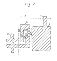
- Fig. 2 shows to a larger scale the part of Fig. 1 ringed by a circle.
- W is a distance parallel to lateral bars 11 and 12 between a side of broken-line rectangle 9, corresponding to an edge of a molded package casing, and a part of inner lead 51 which is perpendicular to the lateral bars and located alongside the stage 3.
- W 2 , W 3 , W 4 and W 5 are, respectively, width of inner lead 51, spacing between inner leads 51 and 52, width of inner lead 52 and spacing between the inner lead 52 and the stage 3, all parallel to lateral bars 11 and 12.
- each distance W has a lower limit, as follows:
- Embodiments of the present invention are intended to provide for an improvement regarding lower limit (2), by connecting inner leadstotie bars by means of support bars, thereby to allow the width of inner leads to reduced to the limit permitted by lead frame fabrication technology.
- Fig. 3 shows a lead frame pattern according to an embodiment of the present invention.
- 11 a and 12a are lateral bars
- 3a is a stage
- 41 a and 42a are stage bars
- 51 a to 58a are inner leads
- 61 a and 62a are tie bars, i.e. parts of an outerframe, for supporting the inner leads in position.
- the parts of the lead frame of Fig. 3 mentioned above are substantially similar to those parts designated by similar reference numerals (without suffix "a") in Fig. 1.
- supporting bars 100a, 101a, 102a and 103a between tips of crank shaped inner leads 51 a, 53a, 55a or 57a, and the tie bars 61 a or 62a, as shown in the small broken-line circles in Fig. 3.
- supporting bar 100a placed between the tip of inner lead 51 a and tie bar 61 a, comprises two bridges 110 and 111 which fix the tip of inner lead 51 a to tie bar 61 a. A hole or hollow portion is left between the two bridges. Thus, it appears as if the inner lead 51a has branches 110 and 111.
- the supporting bars 101a, 102a and 103a are similarly formed.
- the width of the eventual molded package casing is equal to that of the package casing of Fig. 1 (that is, with the same casing size) it is possible to make 1 2 , the distance between the stage 3a and the edge of the casing, smaller than is possible for the frame of Fig. 1. Therefore 1 3 , the width of the stage 3a, can be made wider, and a larger chip can be mounted on the stage. On the other hand, for the same chip size, 1 1 can be made smaller, that is, package size can be reduced.
- packing density factor can be improved.
- the packing density factor can be improved by 20-30% as compared with a lead frame pattern as shown in Fig. 1.
- the molded device is cut away from the outer frame, at the same time the outer leads are separated from each other, and the tips of the outer leads, up to now supported by supporting bars, are cut away from respective supporting bars. Though they are now cut away from the supporting bars, the inner leads are fixed in molded casing and there is no likelihood of deformation.
- the branch portions of inner leads for example bridges 110 and 111 in Fig. 3, are left in the molded casing and provide reinforcement to help keep the tips of the inner leads in position. Though the tips of the branch portions project out slightly from the molded case, this has no effect either upon sealing or upon the characteristics of the IC.
- the outer leads are then bent into a specified shape, in a process exactly the same as for Fig. 1. There is no need to change the process used for assembling the packaged IC. Therefore, the cost of production is no greater.
- Fig. 4 is a plan view of another type of lead frame according to an embodiment of the present invention.
- stage 3b is supported by stage bars 41b and 42b, which are not directly connected to lateral bars 11b and 12b (compare Fig. 3).
- stage bars are fixed to tie bars 61 b and 62b. These tie bars are fixed to lateral bars 11b and 12b.
- the lead frame of Fig. 4 differs from that of Fig. 3 in that additional leads 51c to 58c are provided in Fig. 4 directly extending from lateral bars 11b b and 12b.
- the additional leads are linked to each other by additional tie bars, and their presence makes it possible to provide more connections for (for connecting to bonding pads of) larger or more complicated IC chip circuits.
- stage bars 41 b and 42b are each made up of two bridges similarly to the supporting bars 100b to 103b. It is desirable to minimise stage bar width in order to prevent moisture affecting the IC chip mounted on the stage 3b. Since the stage bars are connected directly to the chip, unlike other leads which are connected to the chip via bonding wire, moisture may penetrate to the chip along the surface of the metal frame along the stage bar. It is thus preferable to make stage bar cross section as small as possible.
- Fig. 5 shows the appearance of a device just after a molding process for forming a molded package casing around a chip is finished.
- the lead frame used is as shown in Fig. 4.
- a chip is mounted on the stage 3b and (its bonding pads) wire bonded to respective inner leads, then the stage 3b is sealed in plastics material.
- Fig. 5 illustrates the leads projecting out from plastic body or casing 300 in which the chip is sealed.
- outer leads are formed by cutting off tie bars and supporting bars. Cutting of these bars is effected along the double-dot chain lines in Fig. 5, so that the portions hatched in the Figure remain in place. These hatched portions 51 b to 58b and 91 b to 98b constitute the outer leads, which are bent and formed as required for the IC concerned.
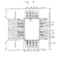
- Fig. 6 shows external appearance of a finished, packaged IC using a lead frame as shown in Fig. 4.
- Fig. 6 (a) is a top plan view
- Fig. 6 (b) is a side view
- Fig. 6 (c) is a bottom plan view of the packaged IC.
- the outer leads are bent inwardly beneath the molded casing, and easy to solder to external circuits.
- This form of IC package is convenient for use with spring connectors.
- This type of IC package is called a plastic chip carrier, and is used widely for small size circuits.
- the packing density factor of IC devices can be increased by applying embodiments - of the present invention.
- the improvement in packing density factor may be 20 to 30%, and this is very significant having regard to recent developments of miniature circuits, which are required to be small as possible. It will be understood that this improvement in packing density factor can represent either a 20%-30% increase in the size of chips which can be accommodated in an area of given size, which means that a large number of elements can be added to each chip, or a 20% to 30% increase in the number of chips of a given size which can be accommodated in an area of given size.
- Embodiments of the present invention do not require any special modifications or special processes for producing packaged devices. Thus, conventional processes and devices can be used for the production of ICs embodying the present invention. Therefore, cost increases are avoided.
- An embodiment of the present invention can provide a lead frame for mounting a semiconductor chip or other semiconductor element, which offers improved packing density, for example for a plastic chip carrier type 5 packaged IC.
- Parts of inner leads located parallel to the stage and the edge of a molded casing of the package, are made as thin as possible. They are fixed to tie bars, until a molding process is finished, by inner lead supporting bars. After the molding process is finished, bars supporting the leads and the stage are cut away. Packing density factor can be improved by about 20-30%.
Landscapes
- Lead Frames For Integrated Circuits (AREA)
Claims (13)
Applications Claiming Priority (2)
| Application Number | Priority Date | Filing Date | Title |
|---|---|---|---|
| JP20549/83 | 1983-02-12 | ||
| JP58020549A JPS59147448A (ja) | 1983-02-12 | 1983-02-12 | 半導体素子搭載用リ−ドフレ−ムおよびこれを用いて製造される半導体装置とその製造方法 |
Publications (3)
| Publication Number | Publication Date |
|---|---|
| EP0118237A2 EP0118237A2 (fr) | 1984-09-12 |
| EP0118237A3 EP0118237A3 (en) | 1986-03-26 |
| EP0118237B1 true EP0118237B1 (fr) | 1989-04-19 |
Family
ID=12030227
Family Applications (1)
| Application Number | Title | Priority Date | Filing Date |
|---|---|---|---|
| EP84300842A Expired EP0118237B1 (fr) | 1983-02-12 | 1984-02-10 | Cadre de convexion pour un élément semi-conducteur |
Country Status (4)
| Country | Link |
|---|---|
| US (1) | US4801997A (fr) |
| EP (1) | EP0118237B1 (fr) |
| JP (1) | JPS59147448A (fr) |
| DE (1) | DE3477864D1 (fr) |
Families Citing this family (19)
| Publication number | Priority date | Publication date | Assignee | Title |
|---|---|---|---|---|
| EP0261324A1 (fr) * | 1986-09-26 | 1988-03-30 | Texas Instruments Incorporated | Boîtier en plastique pour circuit intégré de grandes dimensions |
| JPS6355448U (fr) * | 1986-09-26 | 1988-04-13 | ||
| JPS63120453A (ja) * | 1986-11-08 | 1988-05-24 | Mitsubishi Electric Corp | 混成集積回路装置 |
| US4980219A (en) * | 1988-04-06 | 1990-12-25 | Casio Computer Co., Ltd. | Carrier tape for bonding IC devices and method of using the same |
| US4916519A (en) * | 1989-05-30 | 1990-04-10 | International Business Machines Corporation | Semiconductor package |
| JP2515032B2 (ja) * | 1990-04-18 | 1996-07-10 | 株式会社東芝 | 半導体装置用リ―ドフレ―ム |
| US5114880A (en) * | 1990-06-15 | 1992-05-19 | Motorola, Inc. | Method for fabricating multiple electronic devices within a single carrier structure |
| US5036381A (en) * | 1990-06-15 | 1991-07-30 | Motorola, Inc. | Multiple electronic devices within a single carrier structure |
| JP2877479B2 (ja) * | 1990-09-27 | 1999-03-31 | 株式会社東芝 | 半導体装置用リードフレーム |
| US5150194A (en) * | 1991-04-24 | 1992-09-22 | Micron Technology, Inc. | Anti-bow zip lead frame design |
| US5177591A (en) * | 1991-08-20 | 1993-01-05 | Emanuel Norbert T | Multi-layered fluid soluble alignment bars |
| US5231755A (en) * | 1991-08-20 | 1993-08-03 | Emanuel Technology, Inc. | Method of forming soluble alignment bars |
| US5939775A (en) * | 1996-11-05 | 1999-08-17 | Gcb Technologies, Llc | Leadframe structure and process for packaging intergrated circuits |
| US6048744A (en) * | 1997-09-15 | 2000-04-11 | Micron Technology, Inc. | Integrated circuit package alignment feature |
| US6991960B2 (en) | 2001-08-30 | 2006-01-31 | Micron Technology, Inc. | Method of semiconductor device package alignment and method of testing |
| KR102071078B1 (ko) | 2012-12-06 | 2020-01-30 | 매그나칩 반도체 유한회사 | 멀티 칩 패키지 |
| JP6284397B2 (ja) * | 2014-03-10 | 2018-02-28 | エイブリック株式会社 | 半導体装置及びその製造方法 |
| JP6370071B2 (ja) | 2014-03-19 | 2018-08-08 | エイブリック株式会社 | 半導体装置及びその製造方法 |
| IT202100021638A1 (it) * | 2021-08-10 | 2023-02-10 | St Microelectronics Srl | Procedimento per fabbricare dispositivi a semiconduttore, dispositivo a semiconduttore e assortimento di dispositivi a semiconduttore corrispondenti |
Family Cites Families (10)
| Publication number | Priority date | Publication date | Assignee | Title |
|---|---|---|---|---|
| NL7018378A (fr) * | 1970-12-17 | 1972-06-20 | ||
| US3791025A (en) * | 1972-04-06 | 1974-02-12 | Teledyne Inc | Method of manufacturing an electronic assembly |
| US4066839A (en) * | 1972-11-16 | 1978-01-03 | Sgs-Ates Componenti Elettronici S.P.A. | Molded body incorporating heat dissipator |
| DE2305883A1 (de) * | 1973-02-07 | 1974-08-15 | Finsterhoelzl Rafi Elekt | Leiterplatte |
| US4138691A (en) * | 1977-06-07 | 1979-02-06 | Nippon Electric Co., Ltd. | Framed lead assembly for a semiconductor device comprising insulator reinforcing strips supported by a frame and made integral with lead strips |
| JPS54136179A (en) * | 1978-04-13 | 1979-10-23 | Nec Corp | Semiconductor device |
| JPS5623765A (en) * | 1979-08-01 | 1981-03-06 | Hitachi Ltd | Molded type electronic device |
| US4331740A (en) * | 1980-04-14 | 1982-05-25 | National Semiconductor Corporation | Gang bonding interconnect tape process and structure for semiconductor device automatic assembly |
| JPS5842246A (ja) * | 1981-09-07 | 1983-03-11 | Toshiba Corp | 半導体装置 |
| US4441118A (en) * | 1983-01-13 | 1984-04-03 | Olin Corporation | Composite copper nickel alloys with improved solderability shelf life |
-
1983
- 1983-02-12 JP JP58020549A patent/JPS59147448A/ja active Granted
-
1984
- 1984-02-10 DE DE8484300842T patent/DE3477864D1/de not_active Expired
- 1984-02-10 EP EP84300842A patent/EP0118237B1/fr not_active Expired
-
1988
- 1988-04-19 US US07/185,301 patent/US4801997A/en not_active Expired - Fee Related
Also Published As
| Publication number | Publication date |
|---|---|
| DE3477864D1 (en) | 1989-05-24 |
| US4801997A (en) | 1989-01-31 |
| EP0118237A3 (en) | 1986-03-26 |
| EP0118237A2 (fr) | 1984-09-12 |
| JPS6348430B2 (fr) | 1988-09-29 |
| JPS59147448A (ja) | 1984-08-23 |
Similar Documents
| Publication | Publication Date | Title |
|---|---|---|
| EP0118237B1 (fr) | Cadre de convexion pour un élément semi-conducteur | |
| US6303985B1 (en) | Semiconductor lead frame and package with stiffened mounting paddle | |
| EP0015111B1 (fr) | Cadre conducteur et boîtier pour circuit intégré | |
| EP1662565B1 (fr) | Empaquetage pour semi-conducteur | |
| US5834691A (en) | Lead frame, its use in the fabrication of resin-encapsulated semiconductor device | |
| US7002240B2 (en) | Semiconductor leadframe for staggered board attach | |
| EP0108502A2 (fr) | Dispositif semi-conducteur encapsulé en plastique et procédé pour sa fabrication | |
| EP0228869A2 (fr) | Méthode de fabrication d'un paquetage pour un composant électronique | |
| EP0706213A2 (fr) | Conception d'un cadre de conducteur d'une seule couche ayant une capacité avec un plan de masse | |
| KR100336080B1 (ko) | 반도체 장치 및 그 제조방법 | |
| EP0409196A2 (fr) | Dispositif semi-conducteur du type à encapsulation en plastique | |
| KR20040030283A (ko) | 리드 프레임 및 그 제조 방법 | |
| KR20030035952A (ko) | 리드 프레임과 그 제조 방법 및 그 리드 프레임을 이용한반도체 장치의 제조 방법 | |
| US4633583A (en) | Method of making a lead frame for integrated circuits | |
| US5309018A (en) | Lead frame having deformable supports | |
| US7132314B2 (en) | System and method for forming one or more integrated circuit packages using a flexible leadframe structure | |
| US5393705A (en) | Molded semiconductor device using intermediate lead pattern on film carrier formed from lattice pattern commonly available for devices and process of fabrication thereof | |
| JP2685582B2 (ja) | リードフレーム及びこれを用いた半導体装置 | |
| JPS63296252A (ja) | 樹脂封止型半導体装置 | |
| GB2247988A (en) | Lead frame for semiconductor device | |
| EP0443044A1 (fr) | Cadre de montage pour dispositif a semi-conducteurs et dispositif a semi-conducteurs utilisant ce cadre de montage | |
| US7247515B2 (en) | Frame for semiconductor package | |
| JPH0738036A (ja) | 半導体装置の製造方法 | |
| US5343615A (en) | Semiconductor device and a process for making same having improved leads | |
| JP2515882B2 (ja) | リ―ドフレ―ム、リ―ドフレ―ムの製造方法、半導体装置および半導体装置の製造方法 |
Legal Events
| Date | Code | Title | Description |
|---|---|---|---|
| PUAI | Public reference made under article 153(3) epc to a published international application that has entered the european phase |
Free format text: ORIGINAL CODE: 0009012 |
|
| AK | Designated contracting states |
Designated state(s): DE FR GB |
|
| PUAL | Search report despatched |
Free format text: ORIGINAL CODE: 0009013 |
|
| AK | Designated contracting states |
Kind code of ref document: A3 Designated state(s): DE FR GB |
|
| 17P | Request for examination filed |
Effective date: 19860421 |
|
| 17Q | First examination report despatched |
Effective date: 19880119 |
|
| GRAA | (expected) grant |
Free format text: ORIGINAL CODE: 0009210 |
|
| AK | Designated contracting states |
Kind code of ref document: B1 Designated state(s): DE FR GB |
|
| REF | Corresponds to: |
Ref document number: 3477864 Country of ref document: DE Date of ref document: 19890524 |
|
| ET | Fr: translation filed | ||
| PLBE | No opposition filed within time limit |
Free format text: ORIGINAL CODE: 0009261 |
|
| STAA | Information on the status of an ep patent application or granted ep patent |
Free format text: STATUS: NO OPPOSITION FILED WITHIN TIME LIMIT |
|
| 26N | No opposition filed | ||
| PGFP | Annual fee paid to national office [announced via postgrant information from national office to epo] |
Ref country code: FR Payment date: 19960125 Year of fee payment: 13 |
|
| PGFP | Annual fee paid to national office [announced via postgrant information from national office to epo] |
Ref country code: GB Payment date: 19960201 Year of fee payment: 13 |
|
| PGFP | Annual fee paid to national office [announced via postgrant information from national office to epo] |
Ref country code: DE Payment date: 19960215 Year of fee payment: 13 |
|
| PG25 | Lapsed in a contracting state [announced via postgrant information from national office to epo] |
Ref country code: GB Effective date: 19970210 |
|
| GBPC | Gb: european patent ceased through non-payment of renewal fee |
Effective date: 19970210 |
|
| PG25 | Lapsed in a contracting state [announced via postgrant information from national office to epo] |
Ref country code: FR Effective date: 19971030 |
|
| PG25 | Lapsed in a contracting state [announced via postgrant information from national office to epo] |
Ref country code: DE Effective date: 19971101 |
|
| REG | Reference to a national code |
Ref country code: FR Ref legal event code: ST |