EP0124944A1 - Détecteur de crêtes - Google Patents
Détecteur de crêtes Download PDFInfo
- Publication number
- EP0124944A1 EP0124944A1 EP84200631A EP84200631A EP0124944A1 EP 0124944 A1 EP0124944 A1 EP 0124944A1 EP 84200631 A EP84200631 A EP 84200631A EP 84200631 A EP84200631 A EP 84200631A EP 0124944 A1 EP0124944 A1 EP 0124944A1
- Authority
- EP
- European Patent Office
- Prior art keywords
- voltage
- peak detector
- capacitor
- input
- output
- Prior art date
- Legal status (The legal status is an assumption and is not a legal conclusion. Google has not performed a legal analysis and makes no representation as to the accuracy of the status listed.)
- Granted
Links
- 239000003990 capacitor Substances 0.000 claims abstract description 29
- 238000007599 discharging Methods 0.000 abstract 1
- 238000010586 diagram Methods 0.000 description 13
- 238000005259 measurement Methods 0.000 description 7
- 230000007423 decrease Effects 0.000 description 2
- 230000000306 recurrent effect Effects 0.000 description 2
- 239000004065 semiconductor Substances 0.000 description 2
- 230000003247 decreasing effect Effects 0.000 description 1
- 230000001934 delay Effects 0.000 description 1
- 239000003595 mist Substances 0.000 description 1
Images
Classifications
-
- G—PHYSICS
- G01—MEASURING; TESTING
- G01R—MEASURING ELECTRIC VARIABLES; MEASURING MAGNETIC VARIABLES
- G01R19/00—Arrangements for measuring currents or voltages or for indicating presence or sign thereof
- G01R19/04—Measuring peak values or amplitude or envelope of AC or of pulses
-
- H—ELECTRICITY
- H03—ELECTRONIC CIRCUITRY
- H03D—DEMODULATION OR TRANSFERENCE OF MODULATION FROM ONE CARRIER TO ANOTHER
- H03D1/00—Demodulation of amplitude-modulated oscillations
- H03D1/14—Demodulation of amplitude-modulated oscillations by means of non-linear elements having more than two poles
- H03D1/18—Demodulation of amplitude-modulated oscillations by means of non-linear elements having more than two poles of semiconductor devices
Definitions
- the invention relates to a peak detector comprising a capacitor as a storage element for storing a voltagevalue which as a measure of the peak value of an input voltage to be applied to the peak detector, a voltage comparator circuit having a first input for the input voltage, a second input coupled to the capacitor, and an output, and further comprising a transistor which transistor has its collector coupled to the capacitor and has its base-emitter path coupled both to said output and to a voltage source supplying a voltage E1.
- the voltage comparator circuit comprises a differential amplifier with two transistors in long-tailed pair arrangement and a current mirror arranged in the collector circuit.
- the current source Tr3 constitutes the output of the voltage comparator circuit and is connected in common- emitter arrangement with transistor Tr5 the emitter resistor R4 being connected to a +15 V Power-supply source.
- the latter transistor forms a charging-current source for the capacitor C1 constituting the storage element and is voltage-driven on its base.
- the variation of the charge on the capacitor as a function of the time dt during which a current I flows is equal to the product of the capacitance value C and the capacitor-voltage variation dU: Or:
- a peak detector in accordance with the invention is characterized in that the transistor is operated in common-base arrangement, for which purpose the base is connected to the voltage source and the emitter to said output, and a diode is arranged between the base and the emitter connecting in anti-parallel with the base-emitter diode.
- Such a peak detector may attain a slew rate of some tenths of a volt per nanosecond and measure a pulse of half a volt within an interval of ten to twenty nanoseconds sith an accuracy of substantially one hundred percent.
- the diode across the base-emitter diode limits the voltage across this base-emitter diode to approximately 0.4 V, so that the cross talk via the emitter-collector capacitance is very small.
- a peak detector in accordance with the invention can be extremely suitable for measuring steep non-recurrent pulses of short daration it is desirable to give it a hold function.
- an embodiment may comprise a buffer amplifier which has a high-impedance non-inverting input connected to the capacitor, so that leakage currents can be minimised.
- a buffer amplifier which has a high-impedance non-inverting input connected to the capacitor, so that leakage currents can be minimised.
- the buffer amplifier may be employed in order to shift voltage measurement range.
- Said transistor may be of the NPN-type or of the PNP-type, so that in different combinations negative-going peak values or positive-going peak values an be determined by voltage shifts below or above the zero line.
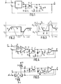
- the peak detector in accordance with the invention shown in Fig. 1 comprises a transistor in common-base arrangement.
- the varying input signal whose positive-going or negative-going peak value is to be measured, is applied to the inpit. 1.
- the input 1 is connected to a first input 2 of a voltage comparator circuit 3, whose second input
- a capacitor 5 which is also connected to the output 6 of the peak detector for the measure peak value and to the collector 7 of the transistor 8 whose base 9 is connected to a voltage source producing a voltage El on a terminal 10.
- the emitter 11 is connected to the output 12 of the voltage comparator circuit 3.
- a diode 13 is arranged in anti-parallel across the base-emitter diode.
- the capacitor 5 may be connected to earth, but as shown, it may alternatively be connected to terminal 14 to which a voltage source producing a voltage E2 is connected.
- a switch 15, represented as a FET can reset the capacitor 5, and consequently the output 6, to a well-defined potential in the present case of value E2, in order to prepare for a new peak-value measurement by means of a reset signal applied to input 16.
- the diagram in Fig. 2 illustrates the operation of the peak detector shown in Fig. 1.
- Transistor 8 is operative only if the output 12 carries a voltage which is some tenths of a volt higher than the value E1 and if moreover, the voltage on the collector 7 and consequently that on the capacitor 5 is lower than the value El.
- the voltage value E2 is substantially lower than the volgage value E1, so that the measurement range for peak values will be situated between E1 and E2, as indicated in Fig. 2.
- the output 12 of the comparator 3 becomes more positive and transistor 8 is turned on, so that capacitor 5 is charged, which gives rise to an increasing voltage on input 4.
- the voltage on inputs 1 and 2 decreases and output 12 supplies a decreasing voltage, so that transistor 8 is cutt off and diode 13 is turned on to limit the voltageswing on the emitter 11.
- the capacitor 5 retains its voltage, so that the voltage on input 4 and output 6 is constant as a fune- tion of time, as indicated by 19 in Fig 2.
- T1 resetting is effected, so that at the instant T2 a new measurement begins with a new peak value at 20.
- El may be selected to be zero, so that for a negative input signal it is possible to measure the smallest value in an absolute sense but this value is negative.
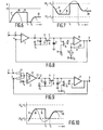
- Fig. 3 indicates how with a suitable choice of the voltages El, E2 and E4 negative-going peak values of an input signal can be measured. Again the voltages E2 and E4 may be zero, so that the highest negative peak values of an input voltage can be determined.
- Fig. 4 shows a circuit arrangement by means of which the diagram of Fig. 3 can be obtained.
- This peak detector is substantially indentical to that shown in Fig. 1, but now there is provided a buffer amplifier 21 with a gain factor of 1 in order to transfer the voltage across the capacitor 5 to the output 6 and the input 4 substantially without leakage.
- the voltage comparator circuit 3 is shown in more detail, in particular to indicate that a voltage inversion is required in order to measure negative-going penk values.
- a differential amplifier 22 whose output 23 is connected to the output 12, and whose non-inverting input 24 is connected to a terminal 25 to which a voltage source providing a voltage E4 is connected.
- the inverting input 26 is connected to input 2 via a resistor 27 and to an input 4 via a resistor 28.
- the circuit operates as follows. If the voltage on input 1 is negative-going after balancing, input 26 becomes negative relative to input 24, so that ouputs 23 and 12 become positive, stransistor 8 is turned on, and the charge on capacitor 5 becomes more positive. The voltage on input 4 increasses, which compensates for the decrease originally occurring at input 26. This means that the circuit follows the negative-going voltage17 in Fig. 3. At the peak 18 transistor 8 is cut off and the circuit holds the voltage value 1Q.
- Fig 5 shows a modified form of the peak detector fo Fig. 1 in more detail.
- the voltage comparator circuit 3 comprises a differential amplifier with transistors 29 and 30 which are emitter-coupled to a current source 31.
- the collector load impedance of transistor 30 is a currnent source 32 which provides a high gain factor and which limits the current to transistor 8.
- the current nirror circuit comprising transistors Tr3 and Tr4 in Fig. 1 of the article mentioned in the introductory part may be used as an alternative. If an even higher gain factor but a smaller bandwidth is desired.
- Fig. 6 shows the diagram associated with the peak detector of Fig. 5.
- the circuit measures positive peak values from zero volts to +5 V.
- the circuit is reset to zero.
- transistor 8 was of the PNP-type. It is also possible to form a peak detector which also measures negative-going or positive-going peak values using a trran- sistor of the NPN-type.
- Fig. 7 shows a diagram identical to the diagram of Fig. 3 but with different voltage limits of the measurement range
- Fig. 8 shows the circuit arrangement of a peak detector with which the diagram shown in Fig. 7 can be obtained and in which transistor 8 is an NPN stransistor.
- the buffer amplifier 21 is provided with negative feedback by means of resistor 33 from the output 6 to the inverting input and resistor 34 from a terminal 35, to which a voltage source producing a voltage E3 may be connected, to the inverting input.
- Fig. 9 is almost identical to Fig. 4, except that transistor 8 is a NPN transistor and capacitor 5 is connected to earth instead of to terminal 14. As a result of the choice of this transistor the voltage values E1 and E2 are interchanged, as will be apparent from Fig. 3 and Fig. 10. However, a signifficant difference between these circuit arrangements together with associated diagrams is that the peak detector shown in Fig. 9 measures positive-going peak values, as can be seen in Fig. 10.
Landscapes
- Physics & Mathematics (AREA)
- Engineering & Computer Science (AREA)
- Power Engineering (AREA)
- Nonlinear Science (AREA)
- General Physics & Mathematics (AREA)
- Measurement Of Current Or Voltage (AREA)
Applications Claiming Priority (2)
| Application Number | Priority Date | Filing Date | Title |
|---|---|---|---|
| NL8301602A NL8301602A (nl) | 1983-05-06 | 1983-05-06 | Topdetector. |
| NL8301602 | 1983-05-06 |
Publications (2)
| Publication Number | Publication Date |
|---|---|
| EP0124944A1 true EP0124944A1 (fr) | 1984-11-14 |
| EP0124944B1 EP0124944B1 (fr) | 1987-11-25 |
Family
ID=19841813
Family Applications (1)
| Application Number | Title | Priority Date | Filing Date |
|---|---|---|---|
| EP84200631A Expired EP0124944B1 (fr) | 1983-05-06 | 1984-05-03 | Détecteur de crêtes |
Country Status (5)
| Country | Link |
|---|---|
| US (1) | US4605867A (fr) |
| EP (1) | EP0124944B1 (fr) |
| JP (1) | JPS59211866A (fr) |
| DE (1) | DE3467816D1 (fr) |
| NL (1) | NL8301602A (fr) |
Cited By (2)
| Publication number | Priority date | Publication date | Assignee | Title |
|---|---|---|---|---|
| WO1999036791A3 (fr) * | 1998-01-15 | 1999-09-16 | Koninkl Philips Electronics Nv | Appareil de detection de cretes |
| RU2506598C1 (ru) * | 2012-07-17 | 2014-02-10 | Российская Федерация, от имени которой выступает Государственная корпорация по атомной энергии "Росатом" | Пиковый детектор |
Families Citing this family (11)
| Publication number | Priority date | Publication date | Assignee | Title |
|---|---|---|---|---|
| JPH0224572A (ja) * | 1988-07-13 | 1990-01-26 | Matsushita Electric Ind Co Ltd | ピークホールド回路 |
| JP2638297B2 (ja) * | 1989-12-25 | 1997-08-06 | 日本電気株式会社 | ピークレベル検出回路 |
| US5304939A (en) * | 1991-06-28 | 1994-04-19 | Digital Equipment Corporation | Tracking peak detector |
| US5362992A (en) * | 1992-06-01 | 1994-11-08 | National Semiconductor Corporation | Electronic control of peak detector response time |
| KR950009777B1 (ko) * | 1992-10-13 | 1995-08-28 | 삼성전자주식회사 | 영상기록재생장치의 기록모드 검출회로 |
| US7161392B2 (en) * | 2004-06-23 | 2007-01-09 | Teradyne, Inc. | Comparator feedback peak detector |
| JP2006211072A (ja) * | 2005-01-26 | 2006-08-10 | Sony Corp | ピークホールド回路及び電子機器 |
| US7439776B1 (en) * | 2006-04-14 | 2008-10-21 | Atheros Communications, Inc. | Technique to increase the speed of a peak detector |
| DE602006013812D1 (de) | 2006-07-25 | 2010-06-02 | St Microelectronics Srl | Vorrichtung zum Vergleich des Spitzenwertes von mindestens einer Spannung mit einer Referenzspannung |
| US20110234775A1 (en) * | 2008-10-20 | 2011-09-29 | Macnaughton Boyd | DLP Link System With Multiple Projectors and Integrated Server |
| US9599643B2 (en) * | 2011-09-29 | 2017-03-21 | Silicon Laboratories Inc. | Peak detector |
Citations (3)
| Publication number | Priority date | Publication date | Assignee | Title |
|---|---|---|---|---|
| US3651419A (en) * | 1970-07-06 | 1972-03-21 | Rca Corp | Peak demodulator |
| DE2233488B1 (de) * | 1972-07-07 | 1973-11-08 | Siemens Ag, 1000 Berlin U. 8000 Muenchen | Demodulator Schaltung mit einem Transistor |
| GB2070781A (en) * | 1980-02-29 | 1981-09-09 | Philips Nv | Peak detector |
-
1983
- 1983-05-06 NL NL8301602A patent/NL8301602A/nl not_active Application Discontinuation
-
1984
- 1984-05-03 DE DE8484200631T patent/DE3467816D1/de not_active Expired
- 1984-05-03 EP EP84200631A patent/EP0124944B1/fr not_active Expired
- 1984-05-04 US US06/607,335 patent/US4605867A/en not_active Expired - Fee Related
- 1984-05-04 JP JP59090064A patent/JPS59211866A/ja active Pending
Patent Citations (3)
| Publication number | Priority date | Publication date | Assignee | Title |
|---|---|---|---|---|
| US3651419A (en) * | 1970-07-06 | 1972-03-21 | Rca Corp | Peak demodulator |
| DE2233488B1 (de) * | 1972-07-07 | 1973-11-08 | Siemens Ag, 1000 Berlin U. 8000 Muenchen | Demodulator Schaltung mit einem Transistor |
| GB2070781A (en) * | 1980-02-29 | 1981-09-09 | Philips Nv | Peak detector |
Non-Patent Citations (1)
| Title |
|---|
| ELECTRONICS, vol. 49, no. 4, 19th February 1976, pages 112-113; New York, US; S. HAYES: "Video detector stores peak for minutes" * |
Cited By (2)
| Publication number | Priority date | Publication date | Assignee | Title |
|---|---|---|---|---|
| WO1999036791A3 (fr) * | 1998-01-15 | 1999-09-16 | Koninkl Philips Electronics Nv | Appareil de detection de cretes |
| RU2506598C1 (ru) * | 2012-07-17 | 2014-02-10 | Российская Федерация, от имени которой выступает Государственная корпорация по атомной энергии "Росатом" | Пиковый детектор |
Also Published As
| Publication number | Publication date |
|---|---|
| NL8301602A (nl) | 1984-12-03 |
| US4605867A (en) | 1986-08-12 |
| DE3467816D1 (en) | 1988-01-07 |
| EP0124944B1 (fr) | 1987-11-25 |
| JPS59211866A (ja) | 1984-11-30 |
Similar Documents
| Publication | Publication Date | Title |
|---|---|---|
| US3054910A (en) | Voltage comparator indicating two input signals equal employing constant current source and bistable trigger | |
| EP0124944A1 (fr) | Détecteur de crêtes | |
| US3902078A (en) | Analog switch | |
| US3985954A (en) | DC level control circuit | |
| US3031588A (en) | Low drift transistorized gating circuit | |
| US3939434A (en) | Wideband DC current amplifier | |
| US3694748A (en) | Peak-to-peak detector | |
| US4307305A (en) | Precision rectifier circuits | |
| EP0484129B1 (fr) | Circuit d'échantillonnage et de maintien | |
| US5831423A (en) | Phase meter and method of providing a voltage indicative of a phase difference | |
| US2914685A (en) | Transistor ramp function generator | |
| US4516041A (en) | Voltage controlled variable capacitor | |
| US3214706A (en) | Wide band amplifier with adjustable d.c. output level | |
| US4625131A (en) | Attenuator circuit | |
| US3949317A (en) | Fast recovery limiting and phase inverting amplifier | |
| US3939365A (en) | Pulse peak detector | |
| ES359795A1 (es) | Una disposicion de circuito electrico. | |
| EP0147584A1 (fr) | Amplificateur différentiel | |
| US3585407A (en) | A complementary transistor switch using a zener diode | |
| US6300804B1 (en) | Differential comparator with dispersion reduction circuitry | |
| US3622883A (en) | Pulsed current transistor beta tester having feedback to maintain emitter to collector current constant | |
| JPH0714141B2 (ja) | パルス発生器 | |
| US3449596A (en) | Video gating circuit | |
| US4010418A (en) | Transistor circuits | |
| US4420698A (en) | Peak detector |
Legal Events
| Date | Code | Title | Description |
|---|---|---|---|
| PUAI | Public reference made under article 153(3) epc to a published international application that has entered the european phase |
Free format text: ORIGINAL CODE: 0009012 |
|
| AK | Designated contracting states |
Designated state(s): DE FR GB NL |
|
| 17P | Request for examination filed |
Effective date: 19841130 |
|
| GRAA | (expected) grant |
Free format text: ORIGINAL CODE: 0009210 |
|
| AK | Designated contracting states |
Kind code of ref document: B1 Designated state(s): DE FR GB NL |
|
| REF | Corresponds to: |
Ref document number: 3467816 Country of ref document: DE Date of ref document: 19880107 |
|
| ET | Fr: translation filed | ||
| PLBE | No opposition filed within time limit |
Free format text: ORIGINAL CODE: 0009261 |
|
| STAA | Information on the status of an ep patent application or granted ep patent |
Free format text: STATUS: NO OPPOSITION FILED WITHIN TIME LIMIT |
|
| 26N | No opposition filed | ||
| PGFP | Annual fee paid to national office [announced via postgrant information from national office to epo] |
Ref country code: NL Payment date: 19900531 Year of fee payment: 7 |
|
| PG25 | Lapsed in a contracting state [announced via postgrant information from national office to epo] |
Ref country code: NL Effective date: 19911201 |
|
| NLV4 | Nl: lapsed or anulled due to non-payment of the annual fee | ||
| PGFP | Annual fee paid to national office [announced via postgrant information from national office to epo] |
Ref country code: GB Payment date: 19920430 Year of fee payment: 9 |
|
| PGFP | Annual fee paid to national office [announced via postgrant information from national office to epo] |
Ref country code: FR Payment date: 19920519 Year of fee payment: 9 |
|
| PGFP | Annual fee paid to national office [announced via postgrant information from national office to epo] |
Ref country code: DE Payment date: 19920724 Year of fee payment: 9 |
|
| PG25 | Lapsed in a contracting state [announced via postgrant information from national office to epo] |
Ref country code: GB Effective date: 19930503 |
|
| GBPC | Gb: european patent ceased through non-payment of renewal fee |
Effective date: 19930503 |
|
| PG25 | Lapsed in a contracting state [announced via postgrant information from national office to epo] |
Ref country code: FR Effective date: 19940131 |
|
| PG25 | Lapsed in a contracting state [announced via postgrant information from national office to epo] |
Ref country code: DE Effective date: 19940201 |
|
| REG | Reference to a national code |
Ref country code: FR Ref legal event code: ST |