EP0143479A1 - Plasma-stimulated chemical vapour deposition device and, in particular, a substrate supporting and electrode disposition and associated components - Google Patents
Plasma-stimulated chemical vapour deposition device and, in particular, a substrate supporting and electrode disposition and associated components Download PDFInfo
- Publication number
- EP0143479A1 EP0143479A1 EP84201441A EP84201441A EP0143479A1 EP 0143479 A1 EP0143479 A1 EP 0143479A1 EP 84201441 A EP84201441 A EP 84201441A EP 84201441 A EP84201441 A EP 84201441A EP 0143479 A1 EP0143479 A1 EP 0143479A1
- Authority
- EP
- European Patent Office
- Prior art keywords
- electrode
- vapour deposition
- electrode plates
- housing
- supporting
- Prior art date
- Legal status (The legal status is an assumption and is not a legal conclusion. Google has not performed a legal analysis and makes no representation as to the accuracy of the status listed.)
- Withdrawn
Links
Images

Classifications
-
- H—ELECTRICITY
- H10—SEMICONDUCTOR DEVICES; ELECTRIC SOLID-STATE DEVICES NOT OTHERWISE PROVIDED FOR
- H10P—GENERIC PROCESSES OR APPARATUS FOR THE MANUFACTURE OR TREATMENT OF DEVICES COVERED BY CLASS H10
- H10P72/00—Handling or holding of wafers, substrates or devices during manufacture or treatment thereof
- H10P72/10—Handling or holding of wafers, substrates or devices during manufacture or treatment thereof using carriers specially adapted therefor, e.g. front opening unified pods [FOUP]
- H10P72/12—Vertical boat type carrier whereby the substrates are horizontally supported, e.g. comprising rod-shaped elements
- H10P72/127—Vertical boat type carrier whereby the substrates are horizontally supported, e.g. comprising rod-shaped elements characterised by the substrate support
-
- C—CHEMISTRY; METALLURGY
- C23—COATING METALLIC MATERIAL; COATING MATERIAL WITH METALLIC MATERIAL; CHEMICAL SURFACE TREATMENT; DIFFUSION TREATMENT OF METALLIC MATERIAL; COATING BY VACUUM EVAPORATION, BY SPUTTERING, BY ION IMPLANTATION OR BY CHEMICAL VAPOUR DEPOSITION, IN GENERAL; INHIBITING CORROSION OF METALLIC MATERIAL OR INCRUSTATION IN GENERAL
- C23C—COATING METALLIC MATERIAL; COATING MATERIAL WITH METALLIC MATERIAL; SURFACE TREATMENT OF METALLIC MATERIAL BY DIFFUSION INTO THE SURFACE, BY CHEMICAL CONVERSION OR SUBSTITUTION; COATING BY VACUUM EVAPORATION, BY SPUTTERING, BY ION IMPLANTATION OR BY CHEMICAL VAPOUR DEPOSITION, IN GENERAL
- C23C16/00—Chemical coating by decomposition of gaseous compounds, without leaving reaction products of surface material in the coating, i.e. chemical vapour deposition [CVD] processes
- C23C16/44—Chemical coating by decomposition of gaseous compounds, without leaving reaction products of surface material in the coating, i.e. chemical vapour deposition [CVD] processes characterised by the method of coating
- C23C16/50—Chemical coating by decomposition of gaseous compounds, without leaving reaction products of surface material in the coating, i.e. chemical vapour deposition [CVD] processes characterised by the method of coating using electric discharges
- C23C16/505—Chemical coating by decomposition of gaseous compounds, without leaving reaction products of surface material in the coating, i.e. chemical vapour deposition [CVD] processes characterised by the method of coating using electric discharges using radio frequency discharges
- C23C16/509—Chemical coating by decomposition of gaseous compounds, without leaving reaction products of surface material in the coating, i.e. chemical vapour deposition [CVD] processes characterised by the method of coating using electric discharges using radio frequency discharges using internal electrodes
-
- H—ELECTRICITY
- H01—ELECTRIC ELEMENTS
- H01J—ELECTRIC DISCHARGE TUBES OR DISCHARGE LAMPS
- H01J37/00—Discharge tubes with provision for introducing objects or material to be exposed to the discharge, e.g. for the purpose of examination or processing thereof
- H01J37/32—Gas-filled discharge tubes
- H01J37/32431—Constructional details of the reactor
Definitions
- Plasma-stimulated chemical vapour deposition device and, in particular, a substrate supporting and electrode disposition and associated components.
- the invention relates to a plasma-stimulated chemical vapour deposition device for the vapour deposition of layers of material on substrates,comprising a housing having an internally defined vapour deposition space and being provided with at least one gas inlet and at least one gas outlet and a gas passage defined between them for reaction gases through the vapour deposition space, if necessary, a heating member for establishing a given raised temperature inside the housing an exhaust member for establishing a given subatmospheric pressure inside the housing, a high-frequency voltage source and a substrate-supporting and electrode disposition, which is or can be arranged in the vapour deposition space of the housing and which comprises a plurality of relatively spaced, sequential electrode plates alternately connected to one terminal and the other terminal of the high-frequency voltage source for establishing, in co-operation with the high-frequency voltage source, a plasma state of the gas in the vapour deposition space of the housing, which electrode plates may serve to support substrates to be processed.
- the substrate-supporting and electrode disposition is formed by a "graphite boat" on wheels, which can thus be rolled in the housing, in particular, in a quartz tube.
- This graphite boat comprises in particular graphite electrodes held spaced apart by insulating spacers.
- the substrates to be processed bear vertically on the vertically arranged graphite electrodes.
- a disadvantage of this known device is that the load depends on the substrate diameter, since with the same tube diamete a larger substrate or water diameter brings about a diminution of the useful reaction surfaces and hence less substrates per load or charge (for example, 108 of 7.6 cm and 30 of 12.7 cm).
- a further disadvantage of the above-mentioned graphite boat is that vapour deposition of conductive materials is not possible.
- the invention has for its object to obviate also this disadvantage and provides for this purpose a preferred embodiment which is furthermore characterized in that the electrode plates are alternately mechanically separated from one another.
- a further disadvantage of the above-mentioned graphite boat is that due to the contact of the graphite boat with the wall of the housing particles are created which give rise to a lower output of semi-conductor devices per processed semi-conductor body as a substrate.
- the invention has furthermore for its object to obviate this disadvantage and provides a preferred embodiment which is characterized in that the substrate-supporting and electrode dispositic is or can be disposed free of the tube wall.
- a further advantageous embodiment of the device in accordance with the invention in particular, of the substrate-supporting and electrode disposition thereof, is characterized in that the electrode plates are provided with fastening members for fastening to at least one respective heat-resistant, rod-shaped,electrically conducting carrier or to at least one respective,electrically insulating carrier provided with an electric conductor, whilst the carriers or their conductors can be connected to a corresponding terminal of the high-frequency voltage source and at least one of the fastening members of each of the electrode plates is designed so that, when fastened, it establishes an electric contact with the respective carrier or its conductor and in that the electrode plates are held spaced apart by means of sleeve-like spacers of heat-resistant, electrically insulating material to be arranged on the rod-shaped carriers.
- a further advantageous embodiment of the device in accordance with.the invention in particular of the substrate-supporting and electrode disposition thereof, is characterized in that at least one electrode plate comprises a basic electrode plate whose top and/or bottom surface is covered at least partly with a layer of heat-resistant, electrically insulating material, preferably quartz.
- the last-mentioned embodiment has the advantage of the presence of a minimum surface of electrode material proper coming into contact with the reaction gases in the processing space.
- a general advantage of the device embodying the present invention is the high capacity independent of the substrate diameter.
- FIG. 1 shows schematically and greatly simplified an embodiment of the plasma-stimulated, chemical vapour deposition device in accordance with the invention.
- a housing 1 in this case a quartz tube, accon dates a substrate-supporting and electrode disposition 3.
- the quai tube 1 is arranged vertically and the substrate-supporting and ele trode disposition 3 comprises a vertical disposition of substantia horizontal, relatively spaced electrode plates 8.
- the electrode plates are alternately connected to one of two conductors 7, whict are connected in turn to the respective terminal of a high-frequer voltage source 5.
- the housing 1 In operation the housing 1 is closed both on the top and the bottom sides and in this case the top side has two gas inlets 4 for reaction gases, whereas the bottom side has one gas outlet 6, which is connected in this case with an exhaust member (not shown) for establishing a subatmospheric pressure inside the housing 1.
- the electrode plates 8 are arranged in a vapour deposition space defined inside the housing 1 and by co-operation witl the high-frequency voltage source 5 a plasma state of the gas pha: is created in operation in the vapour deposition space of the houg ing 1, whilst the electrode plates may serve for supporting substrates 9 to be processed.
- a heating membe: 2 may be provided for creating a given raised temperature inside the housing, particularly in the vapour deposition space.
- the substrate-support. and electrode disposition may be arranged in the housing, which has then to be accessible longitudinally, or it may be arranged vertically in the housing or be removed from the housing.
- the plasma-stimulated chemical vapour deposition device serves to vapour-deposit materials on substrates, which may be se l conductor bodies particularly in the form of substantially circul, discs.
- substrates which may be se l conductor bodies particularly in the form of substantially circul, discs.
- Si0 2 by the plasma reaction of SiH 4 and N 2 0, in which case the Si0 2 may be doped with P by adding PH 3 to the gaseous phase.
- This process is used in the manufacture of photo-voltaic cells and other optical components.
- metal silicides for example, WSi 2 , MoSi 2 , TiSi 2 by the plasma reaction of metal halides with SiH 4 .
- This process is used in the manufacture of the above-mentioned gates for MOS devices and the low-resistance interconnections in particular in large-scale to very large scale integrated circuits.
- Deposition of metal films, for example, A1, Ti, W by pyrolysis is the plasma field of metal compounds, which is used in the connection of components of integrated circuits.
- the substrates can be directly disposed on the electrically conducting electrode plates.
- The.presence of metal material or graphite in the plasma field may give rise to the release of particles which may reduce the yield of semi-conductor devices per substrate.
- a solution of these problems is found in covering at least partly the electrode plates with a heat-resistant, electrically insulating material, preferably quartz.
- a heat-resistant, electrically insulating material preferably quartz.
- one or more of the following materials may be meant: pure kinds of glass such as pyrex glass, alumina, ceramic and silicon carbide.
- a further disadvantage of metallic or graphite electrodes is that they need frequen. cleaning,'which is not the case with a quartz cover; the difference may be a factor 2 to 3. Said solution will also be described with reference to the embodiment to be discussed with reference to Fig. 2.
- one or more -supporting plates of heat-resistant, electrically insulating material for example, quartz may be applied above and in the vicinity of the electrode plate, on which material the substrates are disposed.
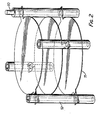
- Fig. 2 shows a possible embodiment of the substrate-supporting and electrode disposition in accordance with the invention, which comprises four cylindrical carriers 10 arranged at the corners of an imaginary rectangle made in this embodiment of heat-resistant, electrically insulating material, preferably quartz, said carriers being provided alongside, for example on the side remote from the electrode plates 11 with an electric conductor to establish contact with the mechanically connected electrode plates as will be described more fully hereinafter.
- the carriers need not necessarily be cylindrical, they may have other shapes of rods, whilst moreover the carriers may be made from heat-resistant, electricallly conducting material so that an electric conductor therein or theron may be omitted. It is necessary for the carriers or, for example, an electrically conducting strip connected therewith to ensure a direct connection of electrode plates with the respective terminal of the high-frequency voltage source.
- the substrate-supporting and electrode disposition shown in Fig. 2 permits of vapour-depositing conductive layers since the electrode plates are alternately connected with a different diametrically opposite pair of rod-shaped carriers, whilst every pair of carriers is connected to one of the terminals of the high-frequency voltage source. It is thus not possible for two sequential electrode plates to establish an electric contact between them due to a precipitate and to a mechanical interconnectior which would involve short circuit of the terminals of the high-frequency voltage source.
- the electrode plates 11 are held spaced apart by sleeve-like spacers 12 of heat-resistant, electrically insulating material, preferably quartz.
- the electrode plates have extensions formed by open eyelets which establish a mechanical and electric contact with the carriers 10 and bear on spacers 12 disposed beneath them.
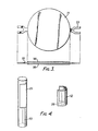
- the design of an electrode plate of this substrate-supporting and electrode disposition is shown in detail in Fig. 3.
- the electrode plate 11 comprises a basic electrode plate 15, for example, of metal or graphite, whose top and/or bottom surface may be covered at least partly with a layer of heat-resistant, electrically insulating material, preferably quartz 14 and 16 respectively.
- the basic electrode material graphite permits of heating the reaction surface by means of a high-frequency coil connected to a high-frequency generator.
- This coil may be arranged outside the quartz tube 1.
- the extensions 13 need not necessarily be coated on the bottom and/or top surface with quartz. If they are,a satisfactory, electric contact should be ensured between the interface 15 and the carriers 10 or, for example, an electrically conducting strip connected herewith.
- the fastening members need not necessarily be open eyelets co-operating with the spacers 12; they may be apertures in the electrode plate co-operating with the spacers 12 or be closed eyelets co-operating with the spacers 12.
- the advantage of the open eyelets is that for removing an electrode plate from the disposition it is not necessary to remove first all superjacent electrode plates and spacers. An upward shift of these parts over a given distance is sufficient to pick the electrode plate concerned out of the disposition.
- the fastening members could have the shape of hooks gripping into the carriers to that apart from a mechanical connection an electric connection is established.
- Fig. 4 shows a carrier 10 and a spacer 12 co-operating one with the other.
- This design of carrier and spacer may be advantageous when for structural reasons precautions are taken by which the spacers cannot be slipped off the top end of a carrier in a vertical direction, for example, in the case illustrated in Fig. 1, where the top ends of the carriers are fastened to the top closure of the housing 1.
- the carriers have at the end or near the end a longitudinal flattened part 25, whilst the spacers 12 have an opening 26 in the circumferential wall matching said flattened part so that the spacers 12 can be arranged in a horizonta movement on the top side of a carrier 20 and be slipped vertically downwards onto the carrier concerned.
- the advantage of'this precaution is that the distance between the electrodes can be varied by choosing spacers of a different length. In this way a variable is obtained, which provides additional possibilities in finding the proper process conditions. Moreover, the various processes requiring a different distance between the electrodes can be carried out by means of the same plasma deposition device, simply by exchanging the original spacers against spacers of a different length.
Landscapes
- Chemical & Material Sciences (AREA)
- Engineering & Computer Science (AREA)
- Physics & Mathematics (AREA)
- Plasma & Fusion (AREA)
- Analytical Chemistry (AREA)
- General Chemical & Material Sciences (AREA)
- Chemical Kinetics & Catalysis (AREA)
- Materials Engineering (AREA)
- Mechanical Engineering (AREA)
- Metallurgy (AREA)
- Organic Chemistry (AREA)
Abstract
A plasma-stimulated chemical vapour deposition device for the vapour deposition of layers of material on substrates, comprising a housing having an internally defined vapour deposition space and being provided with at least one gas inlet and at least one gas outlet and a gas passage defined between them for reaction gases through the vapour deposition space, if necessary a heating member for establishing a given raised temperature inside the housing, an exhaust member for establishing a given subatmospheric pressure inside the housing, a high-frequency voltage source and a substrate-supporting and electrode disposition, which is or can be arranged in the vapour deposition space of the housing and which comprises a plurality of relatively spaced, sequential electrode plates to be alternately connected to one terminal and to the other terminal of the high-frequency voltage source for establishing, in co-operation with the high-frequency voltage source, a plasma state of the gas in the vapour deposition space of the housing, which electrode plates may serve to support substrates to be processed whereby the substrate-supporting and electrode disposition comprises a vertical disposition of substantially horizontal electrode plates.
Description
- Plasma-stimulated chemical vapour deposition device and, in particular, a substrate supporting and electrode disposition and associated components.
- The invention relates to a plasma-stimulated chemical vapour deposition device for the vapour deposition of layers of material on substrates,comprising a housing having an internally defined vapour deposition space and being provided with at least one gas inlet and at least one gas outlet and a gas passage defined between them for reaction gases through the vapour deposition space, if necessary, a heating member for establishing a given raised temperature inside the housing an exhaust member for establishing a given subatmospheric pressure inside the housing, a high-frequency voltage source and a substrate-supporting and electrode disposition, which is or can be arranged in the vapour deposition space of the housing and which comprises a plurality of relatively spaced, sequential electrode plates alternately connected to one terminal and the other terminal of the high-frequency voltage source for establishing, in co-operation with the high-frequency voltage source, a plasma state of the gas in the vapour deposition space of the housing, which electrode plates may serve to support substrates to be processed.
- A device of the kind set forth above is known from an article by Wayne L. Johnson: "Design of plasma deposition reactors" in Solid State Technology, April 1983.
- In this known device the substrate-supporting and electrode disposition is formed by a "graphite boat" on wheels, which can thus be rolled in the housing, in particular, in a quartz tube. This graphite boat comprises in particular graphite electrodes held spaced apart by insulating spacers. The substrates to be processed bear vertically on the vertically arranged graphite electrodes.
- A disadvantage of this known device is that the load depends on the substrate diameter, since with the same tube diamete a larger substrate or water diameter brings about a diminution of the useful reaction surfaces and hence less substrates per load or charge (for example, 108 of 7.6 cm and 30 of 12.7 cm).
- The invention has for its object to obviate said disadvantage of the known device and provides for this purpose a device of the kind set forth in the preamble which is characterized in that the substrate-supporting and electrode disposition comprises a vertical disposition of substantially horizontal electrode plates
- It is noted that per se a plasma-stimulated, chemical vapour deposition device is known from the aforesaid article in which the substrate-supporting and electrode disposition comprises a vertical disposition of two substantially horizontal electrode plates. A disadvantage of this known device is, however, the low capacity,..which disadvantage is likely to be become more serious when larger substrates are used and with a view to the requirements of mass production.
- A further disadvantage of the above-mentioned graphite boat is that vapour deposition of conductive materials is not possible.
- The invention has for its object to obviate also this disadvantage and provides for this purpose a preferred embodiment which is furthermore characterized in that the electrode plates are alternately mechanically separated from one another.
- A further disadvantage of the above-mentioned graphite boat is that due to the contact of the graphite boat with the wall of the housing particles are created which give rise to a lower output of semi-conductor devices per processed semi-conductor body as a substrate.
- The invention has furthermore for its object to obviate this disadvantage and provides a preferred embodiment which is characterized in that the substrate-supporting and electrode dispositic is or can be disposed free of the tube wall.
- A further advantageous embodiment of the device in accordance with the invention, in particular, of the substrate-supporting and electrode disposition thereof, is characterized in that the electrode plates are provided with fastening members for fastening to at least one respective heat-resistant, rod-shaped,electrically conducting carrier or to at least one respective,electrically insulating carrier provided with an electric conductor, whilst the carriers or their conductors can be connected to a corresponding terminal of the high-frequency voltage source and at least one of the fastening members of each of the electrode plates is designed so that, when fastened, it establishes an electric contact with the respective carrier or its conductor and in that the electrode plates are held spaced apart by means of sleeve-like spacers of heat-resistant, electrically insulating material to be arranged on the rod-shaped carriers.
- Owing to the latter aspects simple exchange of the electrode plates can be carried out, whilst by using different lengths of the spacers an optimum electrode distance can be set in a simpler manner.
- A further advantageous embodiment of the device in accordance with.the invention, in particular of the substrate-supporting and electrode disposition thereof, is characterized in that at least one electrode plate comprises a basic electrode plate whose top and/or bottom surface is covered at least partly with a layer of heat-resistant, electrically insulating material, preferably quartz.
- The last-mentioned embodiment has the advantage of the presence of a minimum surface of electrode material proper coming into contact with the reaction gases in the processing space.
- A general advantage of the device embodying the present invention is the high capacity independent of the substrate diameter.
- The invention will now be described more fully with reference to a potential embodiment and the drawing, in which
- Fig. 1 schematically shows a drastically simplified form of a plasma-stimulated, chemical vapour deposition device in accordance with the invention,
- Fig. 2 shows a potential arrangement of the substrate-supporting and electrode disposition embodying the invention,
- Fig. 3 is a plan view and a sectional view of the electrode plate used in the substrate-supporting and electrode disposition and
- Fig. 4 shows an advantageous embodiment of the cylindrical carrier and the spacer of the substrate-supporting and electrode disposition co-operating with the carrier.
- Fig. 1 shows schematically and greatly simplified an embodiment of the plasma-stimulated, chemical vapour deposition device in accordance with the invention. A housing 1, in this case a quartz tube, accon dates a substrate-supporting and electrode disposition 3. The quai tube 1 is arranged vertically and the substrate-supporting and ele trode disposition 3 comprises a vertical disposition of substantia horizontal, relatively spaced electrode plates 8. The electrode plates are alternately connected to one of two conductors 7, whict are connected in turn to the respective terminal of a high-frequer voltage source 5. In operation the housing 1 is closed both on the top and the bottom sides and in this case the top side has two gas inlets 4 for reaction gases, whereas the bottom side has one gas outlet 6, which is connected in this case with an exhaust member (not shown) for establishing a subatmospheric pressure inside the housing 1. The electrode plates 8 are arranged in a vapour deposition space defined inside the housing 1 and by co-operation witl the high-frequency voltage source 5 a plasma state of the gas pha: is created in operation in the vapour deposition space of the houg ing 1, whilst the electrode plates may serve for supporting
substrates 9 to be processed. Finally, if necessary, a heating membe: 2 may be provided for creating a given raised temperature inside the housing, particularly in the vapour deposition space. Between the gas inlet and the gas outlet a passage is formed across the vapour deposition space for reaction gases. The substrate-support. and electrode disposition may be arranged in the housing, which has then to be accessible longitudinally, or it may be arranged vertically in the housing or be removed from the housing. - The plasma-stimulated chemical vapour deposition device serves to vapour-deposit materials on substrates, which may be sel conductor bodies particularly in the form of substantially circul, discs. There follows a non-limitative summary of examples of processes which can be carried out by the plasma-stimulated chemical vapour deposition device embodying the invention.
- Deposition of Si3N4 by the reaction of SiH4 and NH3 in the plasma field.
- Deposition of Si02 by the plasma reaction of SiH4 and N20, in which case the Si02 may be doped with P by adding PH3 to the gaseous phase.
- The aforesaid processes are used in applying electrical insulating layers in the manufacture of integrated circuits and protective layers on said circuits.
- Deposition of polycrystalline Si by pyrolysis in the plasma field of SiH4 or SiH2C12. Also this layer may be dpoed with P, As or B so that a layer of doped poly is obtained.
- The applications of this process are in the domain of gates for metal oxide semi-conductor devices, resistors in integrated circuits and conductive connections between components.
- Deposition of amorphous silicon by pyrolysis of SiH 4*
- This process is used in the manufacture of photo-voltaic cells and other optical components...
- Deposition of metal silicides, for example, WSi2, MoSi2, TiSi2 by the plasma reaction of metal halides with SiH4.
- This process is used in the manufacture of the above-mentioned gates for MOS devices and the low-resistance interconnections in particular in large-scale to very large scale integrated circuits.
- Deposition of metal films, for example, A1, Ti, W by pyrolysis is the plasma field of metal compounds, which is used in the connection of components of integrated circuits.
- Deposition of monocrystalline layers of, for example, Si. These layers may be simultaneously doped with the desired dopant, which process is used in the manufacture of epitaxial layers and PN junctions.
- When conductive layers are vapour-deposited, there is a risk of short-circuiting between neighbouring electrode plates, which can be avoided by alternately separating the electrode plates mechanically one from the other. A potential embodiment of such an arrangement will be described in detail hereinafter with reference, in particular, to Fig. 2.
- In principle the substrates can be directly disposed on the electrically conducting electrode plates. The.presence of metal material or graphite in the plasma field may give rise to the release of particles which may reduce the yield of semi-conductor devices per substrate. A solution of these problems is found in covering at least partly the electrode plates with a heat-resistant, electrically insulating material, preferably quartz. For that matter, where in this description and in the claims reference is made to heat-resistant, electrically insulating material, one or more of the following materials may be meant: pure kinds of glass such as pyrex glass, alumina, ceramic and silicon carbide. A further disadvantage of metallic or graphite electrodes is that they need frequen. cleaning,'which is not the case with a quartz cover; the difference may be a factor 2 to 3. Said solution will also be described with reference to the embodiment to be discussed with reference to Fig. 2.
- As an alternative, one or more -supporting plates of heat-resistant, electrically insulating material, for example, quartz may be applied above and in the vicinity of the electrode plate, on which material the substrates are disposed.
- Fig. 2 shows a possible embodiment of the substrate-supporting and electrode disposition in accordance with the invention, which comprises four
cylindrical carriers 10 arranged at the corners of an imaginary rectangle made in this embodiment of heat-resistant, electrically insulating material, preferably quartz, said carriers being provided alongside, for example on the side remote from theelectrode plates 11 with an electric conductor to establish contact with the mechanically connected electrode plates as will be described more fully hereinafter. The carriers need not necessarily be cylindrical, they may have other shapes of rods, whilst moreover the carriers may be made from heat-resistant, electricallly conducting material so that an electric conductor therein or theron may be omitted. It is necessary for the carriers or, for example, an electrically conducting strip connected therewith to ensure a direct connection of electrode plates with the respective terminal of the high-frequency voltage source. - It is important that the substrate-supporting and electrode disposition shown in Fig. 2 permits of vapour-depositing conductive layers since the electrode plates are alternately connected with a different diametrically opposite pair of rod-shaped carriers, whilst every pair of carriers is connected to one of the terminals of the high-frequency voltage source. It is thus not possible for two sequential electrode plates to establish an electric contact between them due to a precipitate and to a mechanical interconnectior which would involve short circuit of the terminals of the high-frequency voltage source.
- The
electrode plates 11 are held spaced apart by sleeve-like spacers 12 of heat-resistant, electrically insulating material, preferably quartz. In this embodiment the electrode plates have extensions formed by open eyelets which establish a mechanical and electric contact with thecarriers 10 and bear onspacers 12 disposed beneath them. The design of an electrode plate of this substrate-supporting and electrode disposition is shown in detail in Fig. 3. Theelectrode plate 11 comprises abasic electrode plate 15, for example, of metal or graphite, whose top and/or bottom surface may be covered at least partly with a layer of heat-resistant, electrically insulating material, preferablyquartz extensions 13 need not necessarily be coated on the bottom and/or top surface with quartz. If they are,a satisfactory, electric contact should be ensured between theinterface 15 and thecarriers 10 or, for example, an electrically conducting strip connected herewith. - The fastening members need not necessarily be open eyelets co-operating with the
spacers 12; they may be apertures in the electrode plate co-operating with thespacers 12 or be closed eyelets co-operating with thespacers 12. The advantage of the open eyelets is that for removing an electrode plate from the disposition it is not necessary to remove first all superjacent electrode plates and spacers. An upward shift of these parts over a given distance is sufficient to pick the electrode plate concerned out of the disposition. Moreover, the fastening members could have the shape of hooks gripping into the carriers to that apart from a mechanical connection an electric connection is established. - It will also be obvious that it is not necessary to use four carriers and that necessarily two have to be used for establishing an alternating plasma field.
- Fig. 4 shows a
carrier 10 and aspacer 12 co-operating one with the other. This design of carrier and spacer may be advantageous when for structural reasons precautions are taken by which the spacers cannot be slipped off the top end of a carrier in a vertical direction, for example, in the case illustrated in Fig. 1, where the top ends of the carriers are fastened to the top closure of the housing 1. For this purpose the carriers have at the end or near the end a longitudinal flattenedpart 25, whilst thespacers 12 have anopening 26 in the circumferential wall matching said flattened part so that thespacers 12 can be arranged in a horizonta movement on the top side of a carrier 20 and be slipped vertically downwards onto the carrier concerned. - The advantage of'this precaution is that the distance between the electrodes can be varied by choosing spacers of a different length. In this way a variable is obtained, which provides additional possibilities in finding the proper process conditions. Moreover, the various processes requiring a different distance between the electrodes can be carried out by means of the same plasma deposition device, simply by exchanging the original spacers against spacers of a different length.
Claims (12)
1. A plasma-stimulated chemical vapour deposition device for the vapour deposition of layers of material on substrates, comprising a housing having an internally defined vapour deposition space and being provided with at least one gas inlet and at least one gas outlet and a gas passage defined between them for reaction gases through the vapour deposition space, if necessary a heating member for establishing a given raised temperature inside the housing, an exhaust member for establishing a given subatmospheric pressure inside the housing, a high-frequency voltage source and a substrate-supporting and electrode disposition,which is or can be arranged in the vapour deposition space of the housing and which comprises a plurality of relatively spaced, sequential electrode plates to be alternately connected to one terminal and to the other terminal of the high-frequency voltage source for establishing, in co-operation with the high-frequency voltage source, a plasma state of the gas in the vapour deposition space of the housing, which electrode plates may serve to support substrates to be processed characterized in that the substrate-supporting and electrode disposition comprises a vertical disposition of substantially horizontal electrode plates.
2. A device as claimed in Claim 1 characterized in that at least one electrode plate comprises a basic electrode plate whose top and/or bottom surface is covered at least partly with a layer of heat-resistant, electrically insulating material.
3. A device as claimed in Claim 1 characterized in that at least one supporting plate of heat-resistant, electrically insulating material is arranged above at least one electrode plate for supporting a substrate or substrates to be processed.
4. A device as claimed in anyone of the preceding Claims characterized in that the electrode plates and, as the case may be, the associated supporting plate(s) are alternately mechanically separated from one another.
5. ` A device as claimed in anyone of the preceding Claims characterized in that the electrode plates and, as the case may be, the associated supporting plate(s) are provided with fastening members for fastening to at least one respective, heat-resistant, rod-shaped, electrically conducting carrier or to at least one respective, electrically insulating carrier provided with an electric conductor, whilst the carriers or their conductors can be connected to a corresponding terminal of the high-frequency voltage source and at least one of the fastening members of each of the electrode plates is designed so that, when fastened, it establishes an electric contact with the respective carrier or its conductor.
6. A device as claimed in Claim 5 characterized in that the substrate-supporting and electrode disposition comprises four rod-shaped carriers and in that the electrode plates and, as the case may be, the associated supporting plate(s) are alternately connected with a different pair of diametrically opposite, rod-shaped carrier: each pair of carriers being connected to one of the terminals of the high-frequency voltage source.
7. A device as claimed in Claim 5 or 6 characterized in that the electrode plates and, as the case may be, the associated suppori ing plate(s) are held spaced apart by means of sleeve-like spacers of heat-resistant, electrically insulating material to be arranged on the rod-shaped carriers.
8. A device as claimed in Claim 7 characterized in that the rod-shaped carriers are cylindrical and have at the top or in the vicinity thereof a longitudinal flattened part, whilst the spacers have an opening in the circumferential wall matching said flattened part.
9. A device as claimed in anyone of Claims 1 to 8 in which the housing has a tubular shape, characterized in that the substrate supporting and electrode disposition is or can be disposed free of the tube wall.
10. A device as claimed in anyone of Claims 1 to 9 characteriz in that the electrode plates or basic electrode plates are made from aluminium or graphite.
11. A device as claimed in anyone of Claims 2 to 10 characterized in that the heat-resistant, electrically insulating material is quartz.
12. A substrate-supporting and electrode disposition and component parts thereof as claimed in anyone of the preceding Claims.
Applications Claiming Priority (2)
| Application Number | Priority Date | Filing Date | Title |
|---|---|---|---|
| NL8303602A NL8303602A (en) | 1983-10-19 | 1983-10-19 | PLASMA-STIMULATED CHEMICAL VAPOR DEVICE, IN PARTICULAR A SUBSTRATE SUPPORT AND ELECTRODE ARRANGEMENT FOR IT AND ITS COMPONENTS. |
| NL8303602 | 1983-10-19 |
Publications (1)
| Publication Number | Publication Date |
|---|---|
| EP0143479A1 true EP0143479A1 (en) | 1985-06-05 |
Family
ID=19842585
Family Applications (1)
| Application Number | Title | Priority Date | Filing Date |
|---|---|---|---|
| EP84201441A Withdrawn EP0143479A1 (en) | 1983-10-19 | 1984-10-09 | Plasma-stimulated chemical vapour deposition device and, in particular, a substrate supporting and electrode disposition and associated components |
Country Status (2)
| Country | Link |
|---|---|
| EP (1) | EP0143479A1 (en) |
| NL (1) | NL8303602A (en) |
Cited By (19)
| Publication number | Priority date | Publication date | Assignee | Title |
|---|---|---|---|---|
| EP0260097A1 (en) * | 1986-09-09 | 1988-03-16 | Semiconductor Energy Laboratory Co., Ltd. | CVD method and apparatus |
| GB2201162A (en) * | 1987-02-20 | 1988-08-24 | Asm Inc | Electrode boat apparatus for plasma enhanced chemical vapour processing semiconductor wafers |
| EP0313382A1 (en) * | 1987-10-23 | 1989-04-26 | Eaton Corporation | Process for making silicon nitride articles |
| EP0539948A3 (en) * | 1991-10-29 | 1996-01-31 | Canon Kk | Apparatus for forming metal film and process for forming metal film |
| DE19808206A1 (en) * | 1998-02-27 | 1999-09-02 | Gesche | Low pressure gas discharge treatment of wafers for lacquer removal, cleaning or etching |
| WO2002020871A1 (en) * | 2000-09-08 | 2002-03-14 | Centrotherm Elektrische Anlagen Gmbh + Co. | Plasma boat |
| DE102008019023A1 (en) * | 2007-10-22 | 2009-04-23 | Centrotherm Photovoltaics Ag | Vacuum continuous flow system for the processing of substrates |
| TWI481737B (en) * | 2014-08-20 | 2015-04-21 | Powerchip Technology Corp | Bearing fixture |
| WO2015117991A1 (en) * | 2014-02-06 | 2015-08-13 | Kgt Graphit Technologie Gmbh | Protective layer for pecvd graphite boats |
| EP2915901A1 (en) | 2014-03-07 | 2015-09-09 | Roth & Rau AG | Device for plasma processing with process gas circulation in multiple plasmas |
| WO2017005253A1 (en) * | 2015-07-09 | 2017-01-12 | Hanwha Q Cells Gmbh | Device for receiving substrates in pairs |
| EP3367419A1 (en) | 2017-02-28 | 2018-08-29 | Meyer Burger (Germany) AG | Electrode unit with an internal electric network for feeding high frequency voltage and carrier assembly for a plasma processing system |
| CN109082649A (en) * | 2018-09-06 | 2018-12-25 | 深圳市捷佳伟创新能源装备股份有限公司 | A kind of loading device of stable plated film |
| WO2020208146A1 (en) * | 2019-04-10 | 2020-10-15 | Plasmetrex Gmbh | Wafer boat and treatment device for wafers |
| JP2021027342A (en) * | 2019-07-31 | 2021-02-22 | 株式会社Kokusai Electric | Substrate processing device, substrate support tool, and manufacturing method of semiconductor device |
| WO2021142098A1 (en) * | 2020-01-09 | 2021-07-15 | Nordson Corporation | Workpiece support system for plasma treatment and method of using the same |
| CN113130359A (en) * | 2021-04-09 | 2021-07-16 | 深圳市捷佳伟创新能源装备股份有限公司 | Tray and slide glass device |
| US11929272B2 (en) | 2019-07-31 | 2024-03-12 | Kokusai Electric Corporation | Substrate processing apparatus, substrate support, and method of manufacturing semiconductor device |
| CN118407025A (en) * | 2024-05-17 | 2024-07-30 | 重庆欣晖材料技术有限公司 | A component, equipment and carrying device for chemical vapor deposition |
Citations (6)
| Publication number | Priority date | Publication date | Assignee | Title |
|---|---|---|---|---|
| GB1522059A (en) * | 1976-10-19 | 1978-08-23 | Standard Telephones Cables Ltd | Plasma etching |
| DE2810554A1 (en) * | 1977-03-11 | 1978-09-14 | Fujitsu Ltd | METHOD AND DEVICE FOR PLASMA TREATMENT IN SEMI-CONDUCTOR MANUFACTURING |
| US4223048A (en) * | 1978-08-07 | 1980-09-16 | Pacific Western Systems | Plasma enhanced chemical vapor processing of semiconductive wafers |
| EP0016603A1 (en) * | 1979-03-19 | 1980-10-01 | Fujitsu Limited | A method for processing substrate materials by means of treating plasma |
| US4264393A (en) * | 1977-10-31 | 1981-04-28 | Motorola, Inc. | Reactor apparatus for plasma etching or deposition |
| US4287851A (en) * | 1980-01-16 | 1981-09-08 | Dozier Alfred R | Mounting and excitation system for reaction in the plasma state |
-
1983
- 1983-10-19 NL NL8303602A patent/NL8303602A/en not_active Application Discontinuation
-
1984
- 1984-10-09 EP EP84201441A patent/EP0143479A1/en not_active Withdrawn
Patent Citations (6)
| Publication number | Priority date | Publication date | Assignee | Title |
|---|---|---|---|---|
| GB1522059A (en) * | 1976-10-19 | 1978-08-23 | Standard Telephones Cables Ltd | Plasma etching |
| DE2810554A1 (en) * | 1977-03-11 | 1978-09-14 | Fujitsu Ltd | METHOD AND DEVICE FOR PLASMA TREATMENT IN SEMI-CONDUCTOR MANUFACTURING |
| US4264393A (en) * | 1977-10-31 | 1981-04-28 | Motorola, Inc. | Reactor apparatus for plasma etching or deposition |
| US4223048A (en) * | 1978-08-07 | 1980-09-16 | Pacific Western Systems | Plasma enhanced chemical vapor processing of semiconductive wafers |
| EP0016603A1 (en) * | 1979-03-19 | 1980-10-01 | Fujitsu Limited | A method for processing substrate materials by means of treating plasma |
| US4287851A (en) * | 1980-01-16 | 1981-09-08 | Dozier Alfred R | Mounting and excitation system for reaction in the plasma state |
Non-Patent Citations (1)
| Title |
|---|
| SOLID STATE TECHNOLOGY, vol. 22, no. 12, December 1979, pages 88-92; * |
Cited By (29)
| Publication number | Priority date | Publication date | Assignee | Title |
|---|---|---|---|---|
| EP0260097A1 (en) * | 1986-09-09 | 1988-03-16 | Semiconductor Energy Laboratory Co., Ltd. | CVD method and apparatus |
| DE3805293C2 (en) * | 1987-02-20 | 1999-08-05 | Asm Inc | Boat arrangement for holding semiconductor wafers |
| GB2201162A (en) * | 1987-02-20 | 1988-08-24 | Asm Inc | Electrode boat apparatus for plasma enhanced chemical vapour processing semiconductor wafers |
| DE3805293A1 (en) * | 1987-02-20 | 1988-09-01 | Asm Inc | BOAT ARRANGEMENT FOR HOLDING SEMICONDUCTOR DISC |
| NL8702240A (en) * | 1987-02-20 | 1988-09-16 | Asm Inc | ELECTRODE BOAT ASSEMBLY FOR TREATING SEMICONDUCTOR PLATES OR THE LIKE. |
| GB2201162B (en) * | 1987-02-20 | 1991-01-30 | Asm Inc | Electrode boat apparatus for processing semiconductor wafers or the like |
| EP0313382A1 (en) * | 1987-10-23 | 1989-04-26 | Eaton Corporation | Process for making silicon nitride articles |
| EP0539948A3 (en) * | 1991-10-29 | 1996-01-31 | Canon Kk | Apparatus for forming metal film and process for forming metal film |
| US5653810A (en) * | 1991-10-29 | 1997-08-05 | Canon Kabushiki Kaisha | Apparatus for forming metal film and process for forming metal film |
| DE19808206A1 (en) * | 1998-02-27 | 1999-09-02 | Gesche | Low pressure gas discharge treatment of wafers for lacquer removal, cleaning or etching |
| WO2002020871A1 (en) * | 2000-09-08 | 2002-03-14 | Centrotherm Elektrische Anlagen Gmbh + Co. | Plasma boat |
| DE102008019023A1 (en) * | 2007-10-22 | 2009-04-23 | Centrotherm Photovoltaics Ag | Vacuum continuous flow system for the processing of substrates |
| DE102008019023B4 (en) * | 2007-10-22 | 2009-09-24 | Centrotherm Photovoltaics Ag | Vacuum continuous flow system for the processing of substrates |
| WO2015117991A1 (en) * | 2014-02-06 | 2015-08-13 | Kgt Graphit Technologie Gmbh | Protective layer for pecvd graphite boats |
| US10151030B2 (en) | 2014-02-06 | 2018-12-11 | Kgt Graphit Technologie Gmbh | Protective layer for PECVD graphite boats |
| EP2915901A1 (en) | 2014-03-07 | 2015-09-09 | Roth & Rau AG | Device for plasma processing with process gas circulation in multiple plasmas |
| TWI481737B (en) * | 2014-08-20 | 2015-04-21 | Powerchip Technology Corp | Bearing fixture |
| CN108368608A (en) * | 2015-07-09 | 2018-08-03 | 韩华Qcells有限公司 | Equipment for accommodating substrate in pairs |
| WO2017005253A1 (en) * | 2015-07-09 | 2017-01-12 | Hanwha Q Cells Gmbh | Device for receiving substrates in pairs |
| EP3367419A1 (en) | 2017-02-28 | 2018-08-29 | Meyer Burger (Germany) AG | Electrode unit with an internal electric network for feeding high frequency voltage and carrier assembly for a plasma processing system |
| WO2018158013A1 (en) | 2017-02-28 | 2018-09-07 | Meyer Burger (Germany) Ag | Electrode unit having an internal electrical network for supplying high-frequency voltage, and carrier arrangement for a plasma treatment system |
| CN109082649A (en) * | 2018-09-06 | 2018-12-25 | 深圳市捷佳伟创新能源装备股份有限公司 | A kind of loading device of stable plated film |
| WO2020208146A1 (en) * | 2019-04-10 | 2020-10-15 | Plasmetrex Gmbh | Wafer boat and treatment device for wafers |
| JP2021027342A (en) * | 2019-07-31 | 2021-02-22 | 株式会社Kokusai Electric | Substrate processing device, substrate support tool, and manufacturing method of semiconductor device |
| US11929272B2 (en) | 2019-07-31 | 2024-03-12 | Kokusai Electric Corporation | Substrate processing apparatus, substrate support, and method of manufacturing semiconductor device |
| WO2021142098A1 (en) * | 2020-01-09 | 2021-07-15 | Nordson Corporation | Workpiece support system for plasma treatment and method of using the same |
| CN115298797A (en) * | 2020-01-09 | 2022-11-04 | 诺信公司 | Workpiece support system for plasma processing and method of using same |
| CN113130359A (en) * | 2021-04-09 | 2021-07-16 | 深圳市捷佳伟创新能源装备股份有限公司 | Tray and slide glass device |
| CN118407025A (en) * | 2024-05-17 | 2024-07-30 | 重庆欣晖材料技术有限公司 | A component, equipment and carrying device for chemical vapor deposition |
Also Published As
| Publication number | Publication date |
|---|---|
| NL8303602A (en) | 1985-05-17 |
Similar Documents
| Publication | Publication Date | Title |
|---|---|---|
| EP0143479A1 (en) | Plasma-stimulated chemical vapour deposition device and, in particular, a substrate supporting and electrode disposition and associated components | |
| US4287851A (en) | Mounting and excitation system for reaction in the plasma state | |
| EP0002383B1 (en) | Method and apparatus for depositing semiconductor and other films | |
| KR100745942B1 (en) | Inductive coupling plasma processing apparatus | |
| US3151379A (en) | Solar battery and method of making it | |
| EP0049588B1 (en) | Method and apparatus for dry etching and electrostatic chucking device used therein | |
| US9039912B2 (en) | Batch-type remote plasma processing apparatus | |
| CA1090454A (en) | Devices including a layer of amorphous silicon | |
| US5426558A (en) | Anti-stick electrostatic chuck for a low pressure environment | |
| US4452828A (en) | Production of amorphous silicon film | |
| US5748436A (en) | Ceramic electrostatic chuck and method | |
| JPS62125642A (en) | Wafer susceptor | |
| JPH04277648A (en) | Electrostatic chuck coated with diamond | |
| US4741928A (en) | Method for selective deposition of tungsten by chemical vapor deposition onto metal and semiconductor surfaces | |
| US3664874A (en) | Tungsten contacts on silicon substrates | |
| US20070251447A1 (en) | Reactor and Method for Manufacturing Silicon | |
| JPS58155774A (en) | semiconductor equipment | |
| US6177356B1 (en) | Semiconductor cleaning apparatus | |
| JP2013065872A (en) | Manufacturing method of semiconductor device and substrate processing apparatus | |
| JPS5914633A (en) | Plasma cvd apparatus | |
| EP0645828A1 (en) | Process for preparing photovoltaic modules based on crystalline silicon | |
| EP0100611B1 (en) | Reduced capacitance electrode assembly | |
| CN218642817U (en) | Silicon wafer carrier and PECVD reaction chamber | |
| CN115537782B (en) | Silicon wafer carrier and PECVD reaction cavity | |
| JPS62261128A (en) | Manufacture of mos type semiconductor device |
Legal Events
| Date | Code | Title | Description |
|---|---|---|---|
| PUAI | Public reference made under article 153(3) epc to a published international application that has entered the european phase |
Free format text: ORIGINAL CODE: 0009012 |
|
| AK | Designated contracting states |
Designated state(s): AT BE CH DE FR GB IT LI LU NL SE |
|
| 17P | Request for examination filed |
Effective date: 19851114 |
|
| 17Q | First examination report despatched |
Effective date: 19861120 |
|
| STAA | Information on the status of an ep patent application or granted ep patent |
Free format text: STATUS: THE APPLICATION IS DEEMED TO BE WITHDRAWN |
|
| 18D | Application deemed to be withdrawn |
Effective date: 19870330 |