EP0157187A1 - Verstärkerschaltung - Google Patents
Verstärkerschaltung Download PDFInfo
- Publication number
- EP0157187A1 EP0157187A1 EP85102374A EP85102374A EP0157187A1 EP 0157187 A1 EP0157187 A1 EP 0157187A1 EP 85102374 A EP85102374 A EP 85102374A EP 85102374 A EP85102374 A EP 85102374A EP 0157187 A1 EP0157187 A1 EP 0157187A1
- Authority
- EP
- European Patent Office
- Prior art keywords
- amplifier
- transmitter
- circuit
- amplifier circuit
- source
- Prior art date
- Legal status (The legal status is an assumption and is not a legal conclusion. Google has not performed a legal analysis and makes no representation as to the accuracy of the status listed.)
- Granted
Links
Images

Classifications
-
- H—ELECTRICITY
- H03—ELECTRONIC CIRCUITRY
- H03F—AMPLIFIERS
- H03F3/00—Amplifiers with only discharge tubes or only semiconductor devices as amplifying elements
- H03F3/38—DC amplifiers with modulator at input and demodulator at output; Modulators or demodulators specially adapted for use in such amplifiers
-
- H—ELECTRICITY
- H03—ELECTRONIC CIRCUITRY
- H03F—AMPLIFIERS
- H03F1/00—Details of amplifiers with only discharge tubes, only semiconductor devices or only unspecified devices as amplifying elements
- H03F1/34—Negative-feedback-circuit arrangements with or without positive feedback
- H03F1/347—Negative-feedback-circuit arrangements with or without positive feedback using transformers
-
- H—ELECTRICITY
- H03—ELECTRONIC CIRCUITRY
- H03F—AMPLIFIERS
- H03F2200/00—Indexing scheme relating to amplifiers
- H03F2200/372—Noise reduction and elimination in amplifier
Definitions
- the invention relates to a low-distortion audio amplifier circuit, consisting of an amplifier and a source circuit, the source circuit having a current / voltage source and being connected to the amplifier by a transformer.
- Such amplifier circuits have the task of amplifying audio signals as far as possible without distortion and with a small distortion factor. This creates distortions in the audio signal both in the transmitter and in the downstream amplifier.
- the distortions caused by the amplifier can be avoided in a known manner by measures in and on the amplifier.
- the proposed invention does not concern the avoidance of such distortions caused by the amplifier, but only the distortions caused by the transmitter.
- Such an amplifier circuit is known from US Pat. No. 3,828,269, in which the magnetic modulation of the transmitter is kept very small in order to eliminate the distortions that are caused in the transmitter as much as possible. This is achieved by arranging a negative feedback from the output of the amplifier to the transmitter. The transmitter accordingly has a negative feedback coil. The low magnetic modulation of the transmitter induces a low voltage in the coil of the source circuit, which in turn causes the amplifier circuit to have a very low input resistance.
- the disadvantage of this circuit is that the input resistance of this circuit is too low to be able to amplify audio signals from a signal source such as a microphone.
- the correct adaptation of the output resistance of the microphone to the input resistance of the amplifier circuit would be conceivable by installing a resistor in the source circuit, as a result of which the input wi the level would be increased to the desired extent.
- this adaptation in turn has the disadvantage that such a resistance generates noise which is subsequently amplified even further in the amplifier and which is unacceptable for audio signals.
- An amplifier circuit is known from US Pat. No. 3,656,831, in which the source circuit is connected to an amplifier circuit via two trifilar wound transmitters, the output of which is also connected again via a transmitter.
- the amplifier circuit essentially consists of a main amplifier and a fault amplifier. The aim of this arrangement is to correct the distortions that are generated in the main amplifier.
- This amplifier circuit is used in carrier frequency technology.
- the carrier frequency technology relates to the transmission of broadband signals in lines.
- This amplifier circuit is unsuitable for the amplification of audio signals because it has a low input impedance.
- the output impedance on the other hand, which should be low for audio signals, cannot be kept sufficiently low with such an amplifier circuit, since the output circuit and one of the two transmitters in the source circuit are in series.
- the input impedance and the output impedance of this amplifier circuit must be matched to the impedance of the transmission line in question, which means that they are the same, but this is not usable for an audio amplifier circuit.
- the invention solves the problem of creating an audio amplifier circuit fen, which is suitable for signal sources with a large dynamic range and allows a small, light and inexpensive transmitter to be used without having to accept distortions or noise.
- the transmitters can be operated in such an amplifier circuit in such a way that non-linearities of the cores of the transmitters do not take effect.
- the transmitters can be made small, light and cheap.
- high common mode voltages can be kept away from the amplifier.
- the complete insulation enables individual protective earthing of the interconnected devices.
- distortion factor values are achieved at low frequencies that are 10 to 1000 times lower than with known solutions with a completely isolated source circuit.
- the intrinsic noise of the circuit can be made extremely small if the components are selected appropriately.
- the transmitters used in the source group can be made approximately four times smaller and lighter and seven times cheaper than if the transmitter alone had to be dimensioned accordingly to avoid the distortions generated by it.
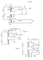
- the source circuit 1 shows an amplifier circuit 1 with a source circuit 2 and an amplifier 3.
- the source circuit 2 consists of a current / voltage source 4 and a resistor 5.
- the current / voltage source 4 can be, for example, an electromechanical converter such as a microphone or another signal source can be provided.
- a transmitter 6 establishes the connection between the amplifier 3 and the current / voltage source 4.
- the secondary winding 8 is connected via lines 9 and 10 to the amplifier 3, so that the lines 9, 10 and the secondary winding 8 together with the amplifier 3 form an input circuit.
- the amplifier 3 has connections 34 and 35 for feeding in a manner known per se.
- An output 11 of the amplifier 3 is connected via a line 12 to the primary winding 13 of a further transmitter 14, the secondary winding 15 of which is in series in the source circuit 2 with the primary winding 7 of the transmitter 6.
- the line 12, together with the further transmitter 14, forms a negative feedback for the amplifier 3.
- the secondary coil 15 has the task of forming a counter voltage to a voltage Ui as it occurs between terminals 32 and 33.
- This counter voltage is in turn generated by an output voltage Ua as it occurs at the output 11 of the amplifier 3 and is thus applied to the primary winding 13 of the further transformer 14.
- the input impedance of the source circuit 2 becomes high. Since the amplifier circuit 1 has only small copper resistances from coils, which belong to the transmitters 6 and 14, it is low-noise.
- the amplifier 3 has a large amplifier. This allows a small voltage across the secondary coil 8, which means that the transmitter 6 is magnetically driven very little and thus also generates only a little distortion.
- the further transformer 14 produces only small distortions because its primary winding 13 is operated by a constant voltage Ua.
- the nonlinear magnetization currents required by the large magnetic modulation of the transmitter 14 are applied by the amplifier 3 without the output voltage Ua becoming nonlinear.
- the transmitter 14 can thus be operated such that the magnetization of the core in the transmitter 14 is close to saturation.
- the other transmitters 14, as for the transmitter 6, also have a small, light and cheap design.
- the amplification of the amplifier 3 is not sufficiently large, the voltage across the secondary coil 8 of the transmitter 6 will not be so small that the distortions generated by the transmitter 6 are small enough. It can also happen that disturbing vibrations occur in the input circuit if the amplification is sufficiently large. Both are prevented in an amplifier circuit 16.
- FIG. 2 shows an amplifier circuit 16 which differs from the amplifier circuit 1 in that the amplifier 3 has a feedback 17 to its inverting input 18. Furthermore, the secondary winding 8 and the non-inverting input 19 of the amplifier 3 are connected to earth. The amplifier 3 together with its feedback 17 forms an amplifier unit 42.
- the amplifier 3 has a very high input impedance in a manner known per se. This is common for operational amplifiers. It can be made arbitrarily small by introducing a resistor 17a as a negative feedback.
- the input impedance of the amplifier unit 42 is equal to the value of the resistor 17a divided by the amplifier of the amplifier 3 not coupled back. If the input impedance of this amplifier unit 42 is made negligibly small, the transmitter 6 works with its secondary winding 8 for an apparent short circuit. The induced voltage in the core of the transmitter 6 is therefore negligible. This also means that no distortions are generated.
- FIG. 3 shows an amplifier circuit 20, in which the amplifier 3 has feedback 17 and 21 on each of the two inputs 18 and 19.
- the non-inverting input 19 is connected to earth via a resistor 22.
- the amplifier 3 with the feedback 17 and 21 forms an amplifier unit 43.
- the input impedance of the amplifier unit 43 can not only be made zero, but also negative.
- the copper resistance of the secondary winding 8 of the transmitter 6 can be partially or even completely compensated, which further reduces the distortions that the transmitter 6 generates.
- R resistance values of the resistors 17, 22 and 37 according to FIG. 3 and Zcu mean the copper resistance of the secondary coil 8.
- the further transformer 14 can then generate certain distortions if the nonlinear magnetizing current at the copper resistor of the primary coil 13 of the further transformer 14 produces a nonlinear voltage drop. As a result, the voltage induced in the source circuit 2 is falsified. This disadvantage can be countered with an amplifier circuit 23 according to FIG.
- An amplifier circuit 23 according to FIG. 4 has an amplifier 3 with feedback 17.
- the negative feedback from the output 11 via the transmitter 14 to the source circuit 2 consists of an amplifier 24, the two inputs 25 and 26 of which each receive feedback 27 and 28 from its output 29 and which also has an input resistor 30 and a resistor 31.
- the feedback 28 preferably has and is a resistor 28a connected to earth via a further resistor 38, but it can also consist of only one line.
- the amplifier 24 with its feedback 27 and 28 and its possible resistors 30, 31 forms an amplifier unit 44.
- the primary winding 13 of the further transmitter 14 is operated by a constant voltage, which means that the source impedance of the amplifier 3 is zero, the corresponding primary coil 13 of the amplifier circuit 23 is powered by a source, ie the amplifier unit 44 operated with a negative source impedance Z. This amounts to:
- R means the values of the individual resistors involved.
- FIG. 5 shows a further amplifier circuit 39 with the source circuit 2 and the two transmitters 6 and 14.
- the transmitter 14 has a further coil 40, which is connected to an output 41.
- the amplifier 3 is connected to the secondary coil 8 in a known manner.
- the line 12 connects the output 11 of the amplifier 3 to the primary coil 13 of the transmitter 14, which is grounded on one side.
- the output voltage of the amplifier 3 is fed back into the source circuit 2 via the line 12 and the primary coil 13.
- the coil 40 picks up this output voltage again and makes it available to the output 41.
- FIG. 6 shows an amplifier circuit 46, which is only to be regarded as a further variant of the amplifier circuit 16 (FIG. 2).
- the feedback 17 is fed back into the transformer 6 with a further coil 47.
- An output 52 of the amplifier unit 42 is provided as a connection for the feedback 17 to the further coil 52.
- the magnetic modulation of the core of the Ueber Carrier 6 brought to zero by the current in the further coil 47. This eliminates the distortion.
- FIG. 7 shows an amplifier circuit 48 with an amplifier unit 49 in the negative feedback, the inverting input 26 of the amplifier 24 being connected via a line 50 to a further coil 51 in the further transformer 14.
- the first transmitter 6 is to be shielded in a known manner in these amplifier circuits. However, its dimensions, which are greatly reduced thanks to the invention, make this considerably easier. Since the further transmitter 14 is voltage-controlled by the amplifier 3, it is not influenced by external fields. Shielding of the transmitter 14 is therefore not necessary.
Landscapes
- Engineering & Computer Science (AREA)
- Power Engineering (AREA)
- Amplifiers (AREA)
Abstract
Description
- Die Erfindung betrifft eine verzerrungsarme Audio-Verstaerkerschaltung, bestehend aus einem Verstaerker und einem Quellenkreis, wobei der Quellenkreis eine Strom/Spannungsquelle aufweist und durch einen Uebertrager an den Verstaerker angeschlossen ist.
- Solche Verstaerkerschaltungen haben die Aufgabe Audio-Signale moeglichst ohne Verzerrungen und bei kleinem Klirrfaktor zu verstaerken. Dabei entstehen Verzerrungen des Audio-Signales sowohl im Uebertrager wie auch im nachgeschalteten Verstaerker. Die durch den Verstaerker hervorgerufenen Verzerrungen lassen sich aber in bekannter Weise durch Massnahmen im und am Verstaerker vermeiden. Die vorgeschlagene Erfindung betrifft aber nicht die Vermeidung solcher durch den Verstaerker hervorgerufener Verzerrungen, sondern nur die durch den Uebertrager verursachten Verzerrungen.
- Aus der US-Patentschrift 3,828,269 ist eine solche Verstaerkerschaltung bekannt, bei der die magnetische Aussteuerung des Uebertragers sehr klein gehalten wird, um die Verzerrungen, die im Uebertrager verursacht werden moeglichst auszuschalten. Dies wird durch die Anordnung einer Gegenkopplung vom Ausgang des Verstaerkers in den Uebertrager erreicht. Der Uebertrager weist dementsprechend eine Gegenkopplungsspule auf. Die geringe magnetische Aussteuerung des Uebertragers induziert in der Spule des Quellenkreises eine geringe Spannung, was wiederum bewirkt, dass die Verstaerkerschaltung einen sehr geringen Eingangswiderstand aufweist.
- Der Nachteil dieser Schaltung besteht darin, dass der Eingangswiderstand dieser Schaltung zu klein ist um Audio-Signale aus einer Signalquelle wie z.B. ein Mikrophon, damit verstaerken zu koennen. Die richtige Anpassung des Ausgangswiderstandes des Mikrophons an den Eingangswiderstand der Verstaerkerschaltung waere zwar denkbar, indem ein Widerstand in den Quellenkreis eingebaut wird, wodurch der Eingangswiderstand im gewuenschten Ausmass erhoeht wuerde. Diese Anpassung hat aber wiederum den Nachteil, dass ein solcher Widerstand Rauschen erzeugt, das nachfolgend im Verstaerker noch weiter verstaerkt wird und das bei Audio-Signalen unannehmbar ist.
- Aus der US-Patentschrift 3,656,831 ist eine Verstaerkerschaltung bekannt, bei der der Quellenkreis ueber zwei trifilar gewickelte Uebertrager an einen Verstaerkerkreis angeschlossen ist, dessen Ausgang auch wieder ueber einen Uebertrager angeschlossen ist. Der Verstaerkerkreis besteht im wesentlichen aus einem Hauptverstaerker und einem Fehlerverstaerker. Ziel dieser Anordnung ist es , die Verzerrungen zu korrigieren, die im Hauptverstaerker erzeugt werden. Diese Verstaerkerschaltung findet in der Traegerfrequenztechnik ihre Anwendung. Die Traegerfrequenztechnik betrifft die Uebertragung breitbandiger Signale in Leitungen.
- Fuer die Verstaerkung von Audio-Signalen ist diese Verstaerkerschaltung ungeeignet, denn sie weist eine niedrige Eingangsimpedanz auf. Die Ausgangsimpedanz dagegen, die fuer Audio-Signale tief sein soll, kann bei einer solchen Verstaerkerschaltung nicht genuegend tief gehalten werden, da der Ausgangskreis und der eine der beiden Uebertrager im Quellenkreis in Serie liegen. Die Eingangsimpedanz und die Ausgangsimpedanz dieser Verstaerkerschaltung muss an die Impedanz der betreffenden Uebertragungsleitung angepasst sein, was bedeutet, dass sie gleich sind, doch dies ist fuer eine Audio-Verstaerkerschaltung nicht brauchbar.
- Es ist ferner an sich bekannt, die Verzerrungen die ein Uebertrager erzeugt dadurch zu vermeiden, dass der Uebertrager gross und schwer ausgebildet wird. Doch diese Loesung ist im Zuge der Miniaturisierung elektronischer Anlagen nicht erwuenscht.
- Die Erfindung, wie sie in den Anspruechen gekennzeichnet ist, loest die Aufgabe, eine Audio-Verstaerkerschaltung zu schaffen, welche sich fuer Signalquellen mit grossem Dynamikbereich eignet und einen kleinen, leichten und billigen Uebertrager einzusetzen erlaubt, ohne dass dafuer Verzerrungen oder Rauschen in Kauf genommen werden muss.
- Die durch die Erfindung erreichten Vorteile sind im wesentlichen darin zu sehen, dass in einer solchen Verstaerkerschaltung die Uebertrager so betrieben werden koennen, dass Nichtlinearitaeten der Kerne der Uebertrager nicht wirksam werden. Dadurch koennen die Uebertrager klein, leicht und billig ausgefuehrt werden. Mit einer solchen Anordnung koennen hohe Gleichtaktspannungen vom Verstaerker fern gehalten werden. Die vollstaendige Isolierung ermoeglicht eine individuelle Schutzerdung der zusammengeschalteten Apparate. Bei tiefen Frequenzen werden auf diese Weise Klirrfaktor-Werte erzielt, die um einen Faktor 10 bis 1000 geringer sind als mit bekannten Loesungen mit vollstaendig isoliertem Quellenkreis. Das Eigenrauschen der Schaltung kann bei geeigneter Wahl der Komponenten verschwindend klein gemacht werden. Die verwendeten Uebertrager im Quellenkreis koennen ungefaehr viermal kleiner und leichter und sieben mal billiger ausgefuehrt werden als wenn der Uebertrager zur Vermeidung der von ihm erzeugten Verzerrungen allein entsprechend dimensioniert werden muesste.
- Im folgenden wird die Erfindung anhand von lediglich einen Ausfuehrungsweg darstellenden Zeichnungen naeher erlaeutert. Es zeigen:
- Figur 1 eine erste Ausfuehrungsform einer erfindungsgemaessen Audio-Verstaerkerschaltung und die
- Figuren 2, 3, 4, 5, 6 und 7 je eine weitere Ausfuehrungsform der Verstaerkerschaltung gemaess Figur 1.
- Aus Figur 1 ist eine Verstaerkerschaltung 1 mit einem Quellenkreis 2 und einem Verstaerker 3 ersichtlich. Der Quellenkreis 2 besteht aus einer Strom/Spannungsquelle 4 und einem Widerstand 5. Als Strom/Spannungsquelle 4 kann beispielsweise ein elektromechanischer Wandler wie z.B. ein Mikrophon oder eine andere Signalquelle vorgesehen sein. Ein Uebertrager 6 stellt die Verbindung zwischen dem Verstaerker 3 und der Strom/Spannungsquelle 4 her. Dessen Primaerwicklung 7 liegt dabei im Quellenkreis 2, dessen Sekundaerwicklung 8 ist ueber Leitungen 9 und 10 an den Verstaerker 3 angeschlossen, so dass die Leitungen 9, 10 und die Sekundaerwicklung 8 zusammen mit dem Verstaerker 3 einen Eingangskreis bilden. Der Verstaerker 3 besitzt in an sich bekannter Weise Anschluesse 34 und 35 fuer eine Speisung. Ein Ausgang 11 des Verstaerkers 3 ist ueber eine Leitung 12 mit der Primaerwicklung 13 eines weiteren Uebertragers 14 verbunden, dessen Sekundaerwicklung 15 im Quellenkreis 2 in Serie zur Primaerwicklung 7 des Uebertragers 6 liegt. Die Leitung 12 bildet zusammen mit dem weiteren Uebertrager 14 eine Gegenkopplung fuer den Verstaerker 3.
- Im Quellenkreis 2 hat die Sekundaerspule 15 die Aufgabe eine Gegenspannung zu bilden zu einer Spannung Ui wie sie zwischen Klemmen 32 und 33 auftritt. Diese Gegenspannung wiederum ist durch eine Ausgangsspannung Ua erzeugt, wie sie am Ausgang 11 des Verstaerkers 3 auftritt und somit an die Primaerwicklung 13 des weiteren Uebertragers 14 angelegt ist. Durch diese Anordnung wird die Eingangsimpedanz des Quellenkreises 2 hoch. Da die Verstaerkerschaltung 1 nur kleine Kupferwiderstaende von Spulen aufweist, die zu den Uebertragern 6 und 14 gehoeren, ist sie rauscharm. Der Verstaerker 3 weist eine grosse Verstaerkung auf. Das erlaubt eine kleine Spannung ueber der Sekundaerspule 8, was bedeutet, dass der Uebertrager 6 magnetisch nur sehr wenig ausgesteuert wird und somit auch nur wenig Verzerrungen erzeugt. Der weitere Uebertrager 14 erzeugt nur kleine Verzerrungen, weil seine Primaerwicklung 13 durch eine konstante Spannung Ua betrieben wird. Die durch die grosse magnetische Aussteuerung des Uebertragers 14 notwendigen nichtlinearen Magnetisierungsstroeme werden vom Verstaerker 3 aufgebracht, ohne dass dabei die Ausgangsspannung Ua nichtlinear wird. Somit kann der Uebertrager 14 so betrieben werden, dass die Magnetisierung des Kerns im Uebertrager 14 nahe an die Saettigung geht. Somit kann fuer den weiteren Uebertrager 14 wie fuer den Uebertrager 6 ebenfalls eine kleine, leichte und billige Ausfuehrung gewaehlt werden.
- Ist die Verstaerkung des Verstaerkers 3 nicht genuegend gross, so wird die Spannung ueber der Sekundaerspule 8 des Uebertragers 6 nicht so klein, dass die Verzerrungen die der Uebertrager 6 erzeugt klein genug sind. Es kann auch vorkommen, dass bei genuegend grosser Verstaerkung stoerende Schwingungen im Eingangskreis auftreten. Beides wird in einer Verstaerkerschaltung 16 verhindert.
- In Figur 2 ist eine Verstaerkerschaltung 16 dargestellt, die sich gegenueber der Verstaerkerschaltung 1 dadurch unterscheidet, dass der Verstaerker 3 eine Rueckkopplung 17 auf seinen invertierenden Eingang 18 aufweist. Weiter ist die Sekundaerwicklung 8 und der nichtinvertierende Eingang 19 des Verstaerkers 3 auf Erde geschaltet. Der Verstaerker 3 bildet zusammen mit seiner Rueckkopplung 17 eine Verstaerkereinheit 42.
- Prinzipiell hat der Verstaerker 3 in an sich bekannter Weise eine sehr hohe Eingangsimpedanz. Diese ist bei Operationsverstaerkern allgemein ueblich. Sie kann beliebig klein gemacht werden, indem man einen Widerstand 17a als Gegenkopplung einfuehrt. Die Eingangsimpedanz der Verstaerkereinheit 42 ist gleich dem Wert des Widerstandes 17a geteilt durch die Verstaerkung des nicht gegengekoppelten Verstaerkers 3. Wird die Eingangsimpedanz dieser Verstaerkereinheit 42 vernachlaessigbar klein gemacht, so arbeitet der Uebertrager 6 mit seiner Sekundaerwicklung 8 auf einen scheinbaren Kurzschluss. Die induzierte Spannung im Kern des Uebertragers 6 ist deshalb verschwindend klein. Dadurch werden auch keine Verzerrungen erzeugt.
- Um moeglichst wenig Rauschen zu erhalten, ist es vorteilhaft, die Rueckkopplung 17 auf einen Abgriff 36 der Sekundaerwicklung 8 zurueckzufuehren.
- In Figur 3 ist eine Verstaerkerschaltung 20 ersichtlich, in welcher der Verstaerker 3 je eine Rueckkopplung 17 und 21 auf beide Eingaenge 18 und 19 aufweist. Der nichtinvertierende Eingang 19 ist ueber einen Widerstand 22 auf Erde geschaltet.
- Der Verstaerker 3 mit den Rueckkopplungen 17 und 21 bildet eine Verstaerkereinheit 43.
- Durch entsprechende Dimensionierung der Rueckkopplungen 17 und 21 kann die Eingangsimpedanz der Verstaerkereinheit 43 nicht nur zu Null, sondern auch negativ gemacht werden. Dadurch kann z.B. der Kupferwiderstand der Sekundaerwicklung 8 des Uebertragers 6 teilweise oder sogar vollstaendig kompensiert werden, was die Verzerrungen die der Uebertrager 6 erzeugt weiter vermindert. Damit dies erreicht ist, gilt:

- Der weitere Uebertrager 14 kann dann gewisse Verzerrungen erzeugen, wenn der nichtlineare Magnetisierungsstrom am Kupferwiderstand der Primaerspule 13 des weiteren Uebertragers 14 einen nichtlinearen Spannungsabfall erzeugt. Dadurch wird die in den Quellenkreis 2 induzierte Spannung verfaelscht. Diesem Nachteil kann mit einer Verstaerkerschaltung 23 gemaess Figur 4 begegnet werden.
- Eine Verstaerkerschaltung 23 gemaess Figur 4 weist einen Verstaerker 3 mit Rueckkopplung 17 auf. Die Gegenkopplung vom Ausgang 11 ueber den Uebertrager 14 auf den Quellenkreis 2 besteht dabei aus einem Verstaerker 24, dessen beide Eingaenge 25 und 26 je eine Rueckkopplung 27 und 28 von dessen Ausgang 29 erhalten und der weiter einen Eingangswiderstand 30 und einen Widerstand 31 aufweist. Die Rueckkopplung 28 weist dabei vorzugsweise einen Widerstand 28a auf und ist ueber einen weiteren Widerstand 38 mit der Erde verbunden, Sie kann aber auch nur aus einer Leitung bestehen. Der Verstaerker 24 mit seinen Rueckkopplungen 27 und 28 und seinen allfaelligen Widerstaenden 30, 31 bildet eine Verstaerkereinheit 44.
- Waehrend in den Verstaerkerschaltungen 1, 16 und 20 die Primaerwicklung 13 des weiteren Uebertragers 14 durch eine konstante Spannung betrieben wird, was bedeutet, dass die Quellenimpedanz des Verstaerkers 3 Null ist, wird die entsprechende Primaerspule 13 der Verstaerkerschaltung 23 durch eine Quelle d.h. die Verstaerkereinheit 44 mit einer negativen Quellenimpedanz Z betrieben. Diese betraegt:

- Dabei bedeuten R die Werte der einzelnen beteiligten Widerstaende. Durch eine Dimensionierung derart, dass die negative Quellenimpedanz Z der Verstaerkereinheit 44 gerade den Kupferwiderstand der Primaerspule 13 des weiteren Uebertragers 14 kompensiert, wird erreicht, dass der nichtlineare Magnetisierungsstrom in der Primaerwicklung 13 keinen Spannungsabfall mehr erzeugt. Damit wird die induzierte Spannung im weiteren Uebertrager 14 verzerrungsfrei. Zur Erzeugung der genannten negativen Quellenimpedanz sind auch andere Ausfuehrungen fuer die Verstaerkereinheit 44 denkbar. Eine davon ist in der Europaeischen Patentanmeldung 0041 472 beschrieben.
- Figur 5 zeigt eine weitere Verstaerkerschaltung 39 mit dem Quellenkreis 2 und den zwei Uebertragern 6 und 14. Der Uebertrager 14 weist eine weitere Spule 40 auf, die mit einem Ausgang 41 verbunden ist. Der Verstaerker 3 ist in bekannter Weise an die Sekundaerspule 8 angeschlossen. Die Leitung 12 verbindet den Ausgang 11 des Verstaerkers 3 mit der einseitig geerdeten Primaerspule 13 des Uebertragers 14.
- Bei dieser Verstaerkerschaltung 39 wird die Ausgangsspannung des Verstaerkers 3 ueber die Leitung 12 und die Primaerspule 13 in den Quellenkreis 2 zurueckgefuehrt. Die Spule 40 greift diese Ausgangsspannung wieder ab und stellt sie dem Ausgang 41 zur Verfuegung.
- Bei der Verstaerkerschaltung 39 wird zunaechst durch schon beschriebene Massnahmen dafuer gesorgt, dass der erste Uebertrager 6 verzerrungsfrei arbeitet. In allen beschriebenen Faellen, wird eine Spannung U 7 ueber der Primaerspule 7 verschwindend klein. Das bedeutet, dass eine Spannung U 15 ueber der Sekundaerspule 15 des weiteren Uebertragers 14 praktisch gleich gross wird, wie die Spannung Ui im Quellenkreis 2 (Fig 1). Da die Spannung U 15 durch die Magnetisierung des Kernes 45 des weiteren Uebertragers 14 erzeugt wird, folgt, dass die induzierte Spannung U 40 in der Spule 40 der Spannung U 15 proportional ist. Da Ui = U 15 und U 40 proportional zu U 15 ist, ergibt sich, dass U 40 proportional zu der Spannung Ui ist. Damit ist eine Verzerrung durch den weiteren Uebertrager 14 ausgeschlossen.
- Alle genannten Anordnungen zur Vermeidung von Verzerrungen in den Uebertragern 6 und 14 sind beliebig miteinander kombinierbar. Insbesondere durch Kombination der Verstaerkerschaltungen 20 und 23 lassen sich die Kupferwiderstaende sowohl der Sekundaerspule 8 wie auch der Primaerspule 13 zusammen ausgleichen. Dies ergibt eine besonders verzerrungsarme und rauscharme Verstaerkerschaltung.
- Figur 6 zeigt eine Verstaerkerschaltung 46, welche lediglich als weitere Variante der Verstaerkerschaltung 16 (Fig 2) zu betrachten ist. Bei dieser Verstaerkerschaltung 46 wird die Rueckkopplung 17 mit einer weiteren Spule 47 in den Uebertrager 6 zurueckgefuehrt. Ein Ausgang 52 der Verstaerkereinheit 42 ist als Anschluss fuer die Rueckkopplung 17 an die weitere Spule 52 vorgesehen. In dieser Verstaerkerschaltung 46 wird die magnetische Aussteuerung des Kernes des Uebertragers 6 durch den Strom in der weiteren Spule 47 zu Null gebracht. Dadurch entfallen die Verzerrungen.
- Figur 7 zeigt eine Verstaerkerschaltung 48 mit einer Verstaerkereinheit 49 in der Gegenkopplung wobei der invertierende Eingang 26 des Verstaerkers 24 ueber eine Leitung 50 mit einer weiteren Spule 51 im weiteren Uebertrager 14 verbunden ist. Durch Gegenkopplung der induzierten Spannung in der weiteren Spule 51 werden nichtlineare Magnetisierungsstroeme unwirksam. Dadurch werden die Verzerrungen sehr gering.
- Der erste Uebertrager 6 ist in diesen Verstaerkerschaltungen in bekannter Weise abzuschirmen. Seine dank der Erfindung stark verminderten Dimensionen erleichtern dies aber erheblich. Da der weitere Uebertrager 14 durch den Verstaerker 3 spannungskontrolliert ist, wird er von Fremdfeldern nicht beeinflusst. Eine Abschirmung des Uebertragers 14 ist deshalb nicht noetig.
Claims (11)
Priority Applications (1)
| Application Number | Priority Date | Filing Date | Title |
|---|---|---|---|
| AT85102374T ATE43211T1 (de) | 1984-03-21 | 1985-03-02 | Verstaerkerschaltung. |
Applications Claiming Priority (2)
| Application Number | Priority Date | Filing Date | Title |
|---|---|---|---|
| CH1415/84 | 1984-03-21 | ||
| CH141584 | 1984-03-21 |
Publications (2)
| Publication Number | Publication Date |
|---|---|
| EP0157187A1 true EP0157187A1 (de) | 1985-10-09 |
| EP0157187B1 EP0157187B1 (de) | 1989-05-17 |
Family
ID=4209913
Family Applications (1)
| Application Number | Title | Priority Date | Filing Date |
|---|---|---|---|
| EP85102374A Expired EP0157187B1 (de) | 1984-03-21 | 1985-03-02 | Verstärkerschaltung |
Country Status (5)
| Country | Link |
|---|---|
| US (1) | US4567443A (de) |
| EP (1) | EP0157187B1 (de) |
| JP (1) | JPH0626286B2 (de) |
| AT (1) | ATE43211T1 (de) |
| DE (1) | DE3570337D1 (de) |
Cited By (1)
| Publication number | Priority date | Publication date | Assignee | Title |
|---|---|---|---|---|
| US7504883B2 (en) | 2006-02-13 | 2009-03-17 | Siemens Aktiengesellschaft | Amplifier device including an operational amplifier, transformer and feedback loop |
Families Citing this family (2)
| Publication number | Priority date | Publication date | Assignee | Title |
|---|---|---|---|---|
| US8036402B2 (en) | 2005-12-15 | 2011-10-11 | Harman International Industries, Incorporated | Distortion compensation |
| US20250300608A1 (en) | 2024-03-22 | 2025-09-25 | Powersoft S.P.A. | Amplifier circuit and method for amplifying an audio signal |
Citations (3)
| Publication number | Priority date | Publication date | Assignee | Title |
|---|---|---|---|---|
| US3249883A (en) * | 1963-06-26 | 1966-05-03 | Beckman Instruments Inc | A. c. coupled pulse amplifier with floating input and grounded output |
| US3656831A (en) * | 1971-01-14 | 1972-04-18 | Bell Telephone Labor Inc | Feedback amplifier |
| US3828269A (en) * | 1972-11-22 | 1974-08-06 | R Norton | Current follower amplifier |
Family Cites Families (2)
| Publication number | Priority date | Publication date | Assignee | Title |
|---|---|---|---|---|
| NL165619C (nl) * | 1972-03-17 | 1981-04-15 | Philips Nv | Getransistoriseerde lijnversterker voor breedbandige informatiesignalen. |
| DE3021007C2 (de) * | 1980-05-31 | 1984-05-17 | ANT Nachrichtentechnik GmbH, 7150 Backnang | Schaltungsanordnung mit Verstärker und Übertrager |
-
1985
- 1985-03-02 EP EP85102374A patent/EP0157187B1/de not_active Expired
- 1985-03-02 DE DE8585102374T patent/DE3570337D1/de not_active Expired
- 1985-03-02 AT AT85102374T patent/ATE43211T1/de not_active IP Right Cessation
- 1985-03-04 US US06/708,171 patent/US4567443A/en not_active Expired - Fee Related
- 1985-03-22 JP JP60057670A patent/JPH0626286B2/ja not_active Expired - Lifetime
Patent Citations (3)
| Publication number | Priority date | Publication date | Assignee | Title |
|---|---|---|---|---|
| US3249883A (en) * | 1963-06-26 | 1966-05-03 | Beckman Instruments Inc | A. c. coupled pulse amplifier with floating input and grounded output |
| US3656831A (en) * | 1971-01-14 | 1972-04-18 | Bell Telephone Labor Inc | Feedback amplifier |
| US3828269A (en) * | 1972-11-22 | 1974-08-06 | R Norton | Current follower amplifier |
Cited By (1)
| Publication number | Priority date | Publication date | Assignee | Title |
|---|---|---|---|---|
| US7504883B2 (en) | 2006-02-13 | 2009-03-17 | Siemens Aktiengesellschaft | Amplifier device including an operational amplifier, transformer and feedback loop |
Also Published As
| Publication number | Publication date |
|---|---|
| JPH0626286B2 (ja) | 1994-04-06 |
| US4567443A (en) | 1986-01-28 |
| JPS60214109A (ja) | 1985-10-26 |
| EP0157187B1 (de) | 1989-05-17 |
| ATE43211T1 (de) | 1989-06-15 |
| DE3570337D1 (en) | 1989-06-22 |
Similar Documents
| Publication | Publication Date | Title |
|---|---|---|
| DE69022108T2 (de) | Verstärkeranordnung. | |
| DE3017521C2 (de) | Zweikanal-Tonleistungsverstärker | |
| DE69425421T2 (de) | Verstärkervorrichtung | |
| EP0087175B1 (de) | Schaltung zur elektronischen Verstärkungsstellung | |
| DE3123735A1 (de) | Stromgesteuerter batteriespeisekreis | |
| DE3036764A1 (en) | Gain control circuit | |
| DE69616234T2 (de) | Vorspannungseinstellung mit transformator | |
| DE2622954C2 (de) | Schaltungsanordnung, die bei der Korrektur von durch Nichtlinearitäten entstandenen Verzerrungen in einem Übertragungssystem anwendbar ist | |
| DE2438883B2 (de) | Durch rueckkopplung stabilisierte verstaerkeranordnung | |
| EP0351639A2 (de) | Eingangsschaltung für Hochfrequenzverstärker | |
| DE2852567C2 (de) | Verstärker mit einem ersten und einem zweiten Verstärkerelement | |
| DE2412031A1 (de) | Gegentaktverstaerker | |
| EP0157187B1 (de) | Verstärkerschaltung | |
| DE2723404A1 (de) | Veraenderlicher entzerrer | |
| DE4104980C2 (de) | Verstärkerstufe für niederohmige Wechselspannungs-Quellen | |
| WO2002001710A1 (de) | Integrierter schaltkreis mit einem analogverstärker | |
| DE10054540B4 (de) | Verstärkerschaltung, insbesondere Leitungstreiber und Verfahren zur Verstärkung eines Signals, insbesondere Verfahren zum Treiben eines Leitungssignals | |
| DE69031686T2 (de) | Ausgangsverstärker | |
| DE863087C (de) | UEbertragungssystem fuer elektrische Signale mit zwei Verstaerkungswegen | |
| DE2257222B2 (de) | Rückgekoppelter Gabel verstärker | |
| DE2838038A1 (de) | Einspeiseeinheit mit hohem ausgangsseitigen innenwiderstand | |
| DE3724980A1 (de) | Spannungswiederholerschaltung fuer eine ohmsche komponente aufweisende last mit kompensation der oberwellenverzerrung | |
| DE826758C (de) | Gegentaktverstaerker | |
| DE3814604A1 (de) | Tonfrequenzverstaerker in brueckenanordnung | |
| DE69432254T2 (de) | Differentielle niederfrequenz-leitungsempfänger |
Legal Events
| Date | Code | Title | Description |
|---|---|---|---|
| PUAI | Public reference made under article 153(3) epc to a published international application that has entered the european phase |
Free format text: ORIGINAL CODE: 0009012 |
|
| AK | Designated contracting states |
Designated state(s): AT BE CH DE FR GB IT LI NL SE |
|
| 17P | Request for examination filed |
Effective date: 19860312 |
|
| 17Q | First examination report despatched |
Effective date: 19871022 |
|
| GRAA | (expected) grant |
Free format text: ORIGINAL CODE: 0009210 |
|
| AK | Designated contracting states |
Kind code of ref document: B1 Designated state(s): AT BE CH DE FR GB IT LI NL SE |
|
| PG25 | Lapsed in a contracting state [announced via postgrant information from national office to epo] |
Ref country code: SE Effective date: 19890517 Ref country code: NL Effective date: 19890517 |
|
| REF | Corresponds to: |
Ref document number: 43211 Country of ref document: AT Date of ref document: 19890615 Kind code of ref document: T |
|
| ITF | It: translation for a ep patent filed | ||
| GBT | Gb: translation of ep patent filed (gb section 77(6)(a)/1977) | ||
| REF | Corresponds to: |
Ref document number: 3570337 Country of ref document: DE Date of ref document: 19890622 |
|
| ET | Fr: translation filed | ||
| NLV1 | Nl: lapsed or annulled due to failure to fulfill the requirements of art. 29p and 29m of the patents act | ||
| PLBE | No opposition filed within time limit |
Free format text: ORIGINAL CODE: 0009261 |
|
| STAA | Information on the status of an ep patent application or granted ep patent |
Free format text: STATUS: NO OPPOSITION FILED WITHIN TIME LIMIT |
|
| 26N | No opposition filed | ||
| ITTA | It: last paid annual fee | ||
| PGFP | Annual fee paid to national office [announced via postgrant information from national office to epo] |
Ref country code: FR Payment date: 19950309 Year of fee payment: 11 |
|
| PGFP | Annual fee paid to national office [announced via postgrant information from national office to epo] |
Ref country code: AT Payment date: 19950313 Year of fee payment: 11 |
|
| PGFP | Annual fee paid to national office [announced via postgrant information from national office to epo] |
Ref country code: BE Payment date: 19950410 Year of fee payment: 11 |
|
| PGFP | Annual fee paid to national office [announced via postgrant information from national office to epo] |
Ref country code: CH Payment date: 19950628 Year of fee payment: 11 |
|
| PG25 | Lapsed in a contracting state [announced via postgrant information from national office to epo] |
Ref country code: AT Effective date: 19960302 |
|
| PGFP | Annual fee paid to national office [announced via postgrant information from national office to epo] |
Ref country code: GB Payment date: 19960307 Year of fee payment: 12 |
|
| PGFP | Annual fee paid to national office [announced via postgrant information from national office to epo] |
Ref country code: DE Payment date: 19960312 Year of fee payment: 12 |
|
| PG25 | Lapsed in a contracting state [announced via postgrant information from national office to epo] |
Ref country code: LI Effective date: 19960331 Ref country code: CH Effective date: 19960331 Ref country code: BE Effective date: 19960331 |
|
| BERE | Be: lapsed |
Owner name: WILLI STUDER A.G. FABRIK FUR ELEKTRONISCHE APPARA Effective date: 19960331 |
|
| REG | Reference to a national code |
Ref country code: CH Ref legal event code: PL |
|
| PG25 | Lapsed in a contracting state [announced via postgrant information from national office to epo] |
Ref country code: FR Effective date: 19961129 |
|
| REG | Reference to a national code |
Ref country code: FR Ref legal event code: ST |
|
| PG25 | Lapsed in a contracting state [announced via postgrant information from national office to epo] |
Ref country code: GB Effective date: 19970302 |
|
| GBPC | Gb: european patent ceased through non-payment of renewal fee |
Effective date: 19970302 |
|
| PG25 | Lapsed in a contracting state [announced via postgrant information from national office to epo] |
Ref country code: DE Effective date: 19971202 |