EP0163081A1 - Procédé de fabrication d'une puce à circuit intégré encapsulée - Google Patents
Procédé de fabrication d'une puce à circuit intégré encapsulée Download PDFInfo
- Publication number
- EP0163081A1 EP0163081A1 EP85104411A EP85104411A EP0163081A1 EP 0163081 A1 EP0163081 A1 EP 0163081A1 EP 85104411 A EP85104411 A EP 85104411A EP 85104411 A EP85104411 A EP 85104411A EP 0163081 A1 EP0163081 A1 EP 0163081A1
- Authority
- EP
- European Patent Office
- Prior art keywords
- support
- chip
- leads
- lead frame
- rails
- Prior art date
- Legal status (The legal status is an assumption and is not a legal conclusion. Google has not performed a legal analysis and makes no representation as to the accuracy of the status listed.)
- Granted
Links
Images


Classifications
-
- H—ELECTRICITY
- H10—SEMICONDUCTOR DEVICES; ELECTRIC SOLID-STATE DEVICES NOT OTHERWISE PROVIDED FOR
- H10W—GENERIC PACKAGES, INTERCONNECTIONS, CONNECTORS OR OTHER CONSTRUCTIONAL DETAILS OF DEVICES COVERED BY CLASS H10
- H10W70/00—Package substrates; Interposers; Redistribution layers [RDL]
- H10W70/01—Manufacture or treatment
- H10W70/04—Manufacture or treatment of leadframes
-
- H—ELECTRICITY
- H10—SEMICONDUCTOR DEVICES; ELECTRIC SOLID-STATE DEVICES NOT OTHERWISE PROVIDED FOR
- H10W—GENERIC PACKAGES, INTERCONNECTIONS, CONNECTORS OR OTHER CONSTRUCTIONAL DETAILS OF DEVICES COVERED BY CLASS H10
- H10W95/00—Packaging processes not covered by the other groups of this subclass
-
- H—ELECTRICITY
- H10—SEMICONDUCTOR DEVICES; ELECTRIC SOLID-STATE DEVICES NOT OTHERWISE PROVIDED FOR
- H10W—GENERIC PACKAGES, INTERCONNECTIONS, CONNECTORS OR OTHER CONSTRUCTIONAL DETAILS OF DEVICES COVERED BY CLASS H10
- H10W70/00—Package substrates; Interposers; Redistribution layers [RDL]
- H10W70/40—Leadframes
- H10W70/411—Chip-supporting parts, e.g. die pads
-
- H—ELECTRICITY
- H10—SEMICONDUCTOR DEVICES; ELECTRIC SOLID-STATE DEVICES NOT OTHERWISE PROVIDED FOR
- H10W—GENERIC PACKAGES, INTERCONNECTIONS, CONNECTORS OR OTHER CONSTRUCTIONAL DETAILS OF DEVICES COVERED BY CLASS H10
- H10W70/00—Package substrates; Interposers; Redistribution layers [RDL]
- H10W70/40—Leadframes
- H10W70/421—Shapes or dispositions
-
- H—ELECTRICITY
- H10—SEMICONDUCTOR DEVICES; ELECTRIC SOLID-STATE DEVICES NOT OTHERWISE PROVIDED FOR
- H10W—GENERIC PACKAGES, INTERCONNECTIONS, CONNECTORS OR OTHER CONSTRUCTIONAL DETAILS OF DEVICES COVERED BY CLASS H10
- H10W72/00—Interconnections or connectors in packages
- H10W72/071—Connecting or disconnecting
-
- H—ELECTRICITY
- H10—SEMICONDUCTOR DEVICES; ELECTRIC SOLID-STATE DEVICES NOT OTHERWISE PROVIDED FOR
- H10W—GENERIC PACKAGES, INTERCONNECTIONS, CONNECTORS OR OTHER CONSTRUCTIONAL DETAILS OF DEVICES COVERED BY CLASS H10
- H10W74/00—Encapsulations, e.g. protective coatings
-
- H—ELECTRICITY
- H10—SEMICONDUCTOR DEVICES; ELECTRIC SOLID-STATE DEVICES NOT OTHERWISE PROVIDED FOR
- H10W—GENERIC PACKAGES, INTERCONNECTIONS, CONNECTORS OR OTHER CONSTRUCTIONAL DETAILS OF DEVICES COVERED BY CLASS H10
- H10W74/00—Encapsulations, e.g. protective coatings
- H10W74/01—Manufacture or treatment
-
- H—ELECTRICITY
- H10—SEMICONDUCTOR DEVICES; ELECTRIC SOLID-STATE DEVICES NOT OTHERWISE PROVIDED FOR
- H10W—GENERIC PACKAGES, INTERCONNECTIONS, CONNECTORS OR OTHER CONSTRUCTIONAL DETAILS OF DEVICES COVERED BY CLASS H10
- H10W90/00—Package configurations
- H10W90/811—Multiple chips on leadframes
Definitions
- This invention concerns lead frames for use with integrated circuit chips.
- the manufacture of such lead frames is disclosed in, for example, the following U.S. patents: 4,204,317; 4,137,546; 3,750,277; 3,537,175; 3,469,953.
- an IC chip After an IC chip has been mounted' on a lead frame chip carrier, and electrically connected to the leads thereof, it is often packaged in encapsulating material.
- Such packaged chip-containing lead frames are shown in, for example, the following U.S.
- the lead frames are usually made by stamping or etching metal strips. Where the manufactured quantities are sufficiently great, stamping is preferred because of its lower cost.
- stamping is carried out in progressive dies; that is, a metal strip is fed through a stamping press having successive punch and die sets at a number of stations, where successive stamping operations are carried out.
- a lead frame having 68 leads would require about 15 to 20 stamping stations and about 140 to 150 cuts.
- the number of required stamping stations and cuts the difficulty in maintaining adequate quality of the stamped lead frames also increases.
- This invention can reduce the number of required stamping stations and cuts per lead frame. This is accomplished by not making an entire lead frame out of one integral metal strip, as was done in the prior art. Instead, the lead frame is fabricated from a plurality of individual segments which can be fabricated from the same set of stamping tools. Thus, if two segments are used per lead frame, the number of stamping stations can be about halved and the number of cuts can be reduced even more. And if four segments are used per lead frame, the number of stamping stations and cuts can be reduced an even greater extent.
- the lead frame is manufactured by assembling the segments with precise positioning, and then securing the segments in a suitable support to maintain said precise positions. An IC chip can then be disposed thereon and electrically connected to the leads.
- This invention is particularly concerned with the manufacture of an encapsulated IC chip which permits electrical testing thereof prior to encapsulation. Thus, in many cases, faults, such as poor electrical connections can be repaired prior to encapsulation.
- Fig. 1 shows a lead frame segment after stamping and Fig. 2 shows a strip of such lead frame segments.
- substantially identical lead frame segments 1 were stamped from a lonc metal strip, as shown in F' . 2.
- segment 1 s shown in Fig. 1 .
- segments 1 were stamped from 10 mil copper alloy, specifically, Olin CDA194, and were maintained in strip form by means of continuous rails 2 and 3, as shown in Fig. 2. Between segments 1, there were support bars 35 extending from rail 3 to rail 2.
- Each segment 1 comprised seventeen leads 4.
- the inner ends 5 of leads 4, which would eventually be electrically connected to an IC chip, were 9 mils wide and spaced 9 mils apart.
- the widest parts 6 of leads 4 were inward from the outer ends 7 thereof and were 28 mils wide spaced 22 mils apart. Outer ends 7 were 18 mils wide spaced 32 mils apart.
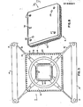
- Support 11 for this example was made of a high temperature thermoplastic material, specifically, a polyetherimide resin made by General Electric Co., Pittsfield, Mass., under the trade name Ultem.
- a recess 12 in which an IC chip would eventually be disposed.
- Recess 12 was 340 mils square and was recessed 8 mils below surface 13 of support 11.
- Surrounding recess 12 were seventy-two raised projections 14, eighteen per side. Projections 14 were 7 mils wide by 25 mils long by 9 mils high. Spaces 15 between the projections were 11 mils wide. At assembly of segments 1 to support 11, narrow ends 5 of leads 4 would lie on surface 13 in spaces 15 between projections 14.
- each projection 14 On the inner end of each projection 14 was another raised portion 16, measuring 7 mils wide by 10 mils long by 6 mils high. Raised portions 16 provided means for securing the leads in spaces 15 by, for example heating and slightly flowing plastic portions 16 over the leads. There was an encircling trough 17 outside the perimeter formed by all the projections 14.
- slots 18 were formed by projections 29 which were similar to projections 14 but bigger. Projections 29 were 20 mils wide by 32 mils long by 9 mils high. Slots 18 were 30 -mils wide. There were raised portions 30 on the inner ends of projections 29, similar to raised portions 16 on projections 14. Raised portions 30 were 20 mils wide by 10 mils long by 6 mils high.
- Rails 19 In order to permit supports 11 to be processed in existing manufacturing equipment for chip-carrying lead frames, there were rails 19, compatible with said equipment, spaced from each side of support 11 and connected thereto by tie bars 20. Rails 19 were 10 mils thick by 135 mils wide and were 1.400 inches apart from each other. Boles 21 provided means for accurate positioning of the supports during indexing. There were four posts 22 on support 11 for accurate mating of support 11 with cover 23, which was made of the same plastic as support 11.
- Cover 23 had a recess 24 to mate with recess 12, and had an additional recess 25 to accommodate projections 14. Cover 23 also had a trough 26 to mate with trough 17, and four holes 27 into which posts 22 fit. There were also two holes 28 connecting with trough 26. After assembly of cover 23 onto support 11, a sealant material could be injected into holes 28 to fill troughs 17 and 26 in order to seal the IC chip from the environment.
- an IC chip 31, shown in dotted lines in Fig. 5, would be conventionally attached in the pad area, recess 12, and would be conventionally electrically connected to ends 5 of leads 4.
- the rail construction of support 11 permits this processing to be performed on existing chip-carrier lead frame processing equipment.
- An advantage of this invention is that the IC chip and package can now be tested for electrical characteristics, because all sixty-eight leads are now electrically isolated, and repair of electrical connections can be made, if necessary. In the past, such repair could not be made because the leads were not electrically isolated until after packaging.
- the external ends of leads 4 can now be formed into a desired shape, such as "J" lead shape 34 shown in Figs. 5 and 8.
- cover 23 is placed on support 11, posts 22 fitting into holes 27.
- Holes 27 are counterbored about half-way through as shown in Fig. 7, for example, to 43 mils diameter from 33 mils diameter.
- Posts 27 extend somewhat in the counterbores of holes 27, thereby providing the means for securing cover 23 to support 11 by heat-flowing the extending upper ends of posts 27, as raised portions 16 and 30 were heat-flowed.
- a sealant for example, a silicone gel, is pumped into boles 28 to completely fill troughs 17 and 28 as well as holes 28.
- the sealant should be sufficiently adherent and flexible, after curing, to maintain a hermetic seal through normal thermal cycling requirements.
- cover 23 and sealing of trough 17 and 28 can be performed in an atmosphere having greater heat dissipation characteristics than air such as helium. This atmosphere will be sealed in the recesses in which chip 31 is disposed.
- a lead identifier 32 may be used, as shown in Fig. 8, and rails 19 and tie bars 20 are removed at score lines 33.
- the finished unit shown in Fig. 8, had overall measurements, including formed leads 34, of 988 mils square by 175 mils high.
- This invention is also applicable to lead frames made other than by stamping, such as etching or chemical forming. There, a significant advantage to the use of segments as per this invention is a substantial reduction in tooling cost.
Landscapes
- Lead Frames For Integrated Circuits (AREA)
- Credit Cards Or The Like (AREA)
- Testing Or Measuring Of Semiconductors Or The Like (AREA)
- Encapsulation Of And Coatings For Semiconductor Or Solid State Devices (AREA)
Priority Applications (1)
| Application Number | Priority Date | Filing Date | Title |
|---|---|---|---|
| AT85104411T ATE49680T1 (de) | 1984-05-02 | 1985-04-11 | Verfahren zum herstellen eines gekapselten icpl|ttchens. |
Applications Claiming Priority (2)
| Application Number | Priority Date | Filing Date | Title |
|---|---|---|---|
| US60631084A | 1984-05-02 | 1984-05-02 | |
| US606310 | 1984-05-02 |
Publications (2)
| Publication Number | Publication Date |
|---|---|
| EP0163081A1 true EP0163081A1 (fr) | 1985-12-04 |
| EP0163081B1 EP0163081B1 (fr) | 1990-01-17 |
Family
ID=24427458
Family Applications (1)
| Application Number | Title | Priority Date | Filing Date |
|---|---|---|---|
| EP85104411A Expired - Lifetime EP0163081B1 (fr) | 1984-05-02 | 1985-04-11 | Procédé de fabrication d'une puce à circuit intégré encapsulée |
Country Status (5)
| Country | Link |
|---|---|
| EP (1) | EP0163081B1 (fr) |
| JP (1) | JPS60240133A (fr) |
| KR (1) | KR850008047A (fr) |
| AT (1) | ATE49680T1 (fr) |
| DE (1) | DE3575497D1 (fr) |
Cited By (2)
| Publication number | Priority date | Publication date | Assignee | Title |
|---|---|---|---|---|
| DE4411973A1 (de) * | 1993-04-07 | 1994-10-20 | Samsung Electronics Co Ltd | KGD-Anordnung |
| KR101253533B1 (ko) * | 2007-05-31 | 2013-04-11 | 퀄컴 인코포레이티드 | 향상된 타이밍 마진을 위해 지연 추적을 이용한 메모리 디바이스 |
Citations (4)
| Publication number | Priority date | Publication date | Assignee | Title |
|---|---|---|---|---|
| US4137546A (en) * | 1977-10-14 | 1979-01-30 | Plessey Incorporated | Stamped lead frame for semiconductor packages |
| GB2027990A (en) * | 1978-08-02 | 1980-02-27 | Hitachi Ltd | Lead-frame for a semiconductor device |
| EP0023165A1 (fr) * | 1979-07-17 | 1981-01-28 | Thomson-Csf | Plate-forme support de grille de connexion, notamment pour boîtier de circuits intégrés, et boîtier comportant une telle plate-forme |
| DE3112564A1 (de) * | 1980-03-31 | 1982-06-03 | VLSI Technology Research Association, Kawasaki, Kanagawa | Gekapselte halbleiteranordnung |
-
1985
- 1985-04-11 EP EP85104411A patent/EP0163081B1/fr not_active Expired - Lifetime
- 1985-04-11 DE DE8585104411T patent/DE3575497D1/de not_active Expired - Lifetime
- 1985-04-11 AT AT85104411T patent/ATE49680T1/de not_active IP Right Cessation
- 1985-05-01 JP JP60092399A patent/JPS60240133A/ja active Pending
- 1985-05-01 KR KR1019850002954A patent/KR850008047A/ko not_active Withdrawn
Patent Citations (4)
| Publication number | Priority date | Publication date | Assignee | Title |
|---|---|---|---|---|
| US4137546A (en) * | 1977-10-14 | 1979-01-30 | Plessey Incorporated | Stamped lead frame for semiconductor packages |
| GB2027990A (en) * | 1978-08-02 | 1980-02-27 | Hitachi Ltd | Lead-frame for a semiconductor device |
| EP0023165A1 (fr) * | 1979-07-17 | 1981-01-28 | Thomson-Csf | Plate-forme support de grille de connexion, notamment pour boîtier de circuits intégrés, et boîtier comportant une telle plate-forme |
| DE3112564A1 (de) * | 1980-03-31 | 1982-06-03 | VLSI Technology Research Association, Kawasaki, Kanagawa | Gekapselte halbleiteranordnung |
Cited By (3)
| Publication number | Priority date | Publication date | Assignee | Title |
|---|---|---|---|---|
| DE4411973A1 (de) * | 1993-04-07 | 1994-10-20 | Samsung Electronics Co Ltd | KGD-Anordnung |
| DE4411973C2 (de) * | 1993-04-07 | 2003-07-03 | Samsung Electronics Co Ltd | KGD-Anordnung und Verfahren zur Herstellung einer KGD-Anordnung |
| KR101253533B1 (ko) * | 2007-05-31 | 2013-04-11 | 퀄컴 인코포레이티드 | 향상된 타이밍 마진을 위해 지연 추적을 이용한 메모리 디바이스 |
Also Published As
| Publication number | Publication date |
|---|---|
| DE3575497D1 (de) | 1990-02-22 |
| JPS60240133A (ja) | 1985-11-29 |
| EP0163081B1 (fr) | 1990-01-17 |
| ATE49680T1 (de) | 1990-02-15 |
| KR850008047A (ko) | 1985-12-11 |
Similar Documents
| Publication | Publication Date | Title |
|---|---|---|
| US4653174A (en) | Method of making packaged IC chip | |
| US4820658A (en) | Method of making a packaged IC chip | |
| US4554404A (en) | Support for lead frame for IC chip carrier | |
| US4663650A (en) | Packaged integrated circuit chip | |
| US4079511A (en) | Method for packaging hermetically sealed integrated circuit chips on lead frames | |
| US4012766A (en) | Semiconductor package and method of manufacture thereof | |
| US4026008A (en) | Semiconductor lead structure and assembly and method for fabricating same | |
| US3611061A (en) | Multiple lead integrated circuit device and frame member for the fabrication thereof | |
| US5114880A (en) | Method for fabricating multiple electronic devices within a single carrier structure | |
| US4663651A (en) | Segmented lead frame strip for IC chip carrier | |
| EP0331814B1 (fr) | Cadre conducteur pour dispositif semi-conducteur | |
| US3650648A (en) | System for molding electronic components | |
| US3716764A (en) | Process for encapsulating electronic components in plastic | |
| US5384286A (en) | Process for encapsulating a semiconductor chip, leadframe and heatsink | |
| US7786554B2 (en) | Stress-free lead frame | |
| US5963796A (en) | Fabrication method for semiconductor package substrate and semiconductor package | |
| EP0163856A1 (fr) | Procédé de fabrication d'un support de cadre d'interconnexions pour une puce à circuit intégré | |
| WO1992014263A1 (fr) | Cadre de support pour modules a semi-conducteurs | |
| EP0163081B1 (fr) | Procédé de fabrication d'une puce à circuit intégré encapsulée | |
| US5036381A (en) | Multiple electronic devices within a single carrier structure | |
| EP0163082A1 (fr) | Puce à circuit intégré montée dans un boîtier | |
| EP0163077B1 (fr) | Procédé de fabrication d'une puce à circuit intégré montée dans un boîtier | |
| US4611398A (en) | Integrated circuit package | |
| US6867483B2 (en) | Stress-free lead frame | |
| US5521124A (en) | Method of fabricating plastic transfer molded semiconductor silicone bridge rectifiers with radial terminals |
Legal Events
| Date | Code | Title | Description |
|---|---|---|---|
| PUAI | Public reference made under article 153(3) epc to a published international application that has entered the european phase |
Free format text: ORIGINAL CODE: 0009012 |
|
| 17P | Request for examination filed |
Effective date: 19850411 |
|
| AK | Designated contracting states |
Designated state(s): AT BE DE FR GB IT NL |
|
| 17Q | First examination report despatched |
Effective date: 19870911 |
|
| ITF | It: translation for a ep patent filed | ||
| GRAA | (expected) grant |
Free format text: ORIGINAL CODE: 0009210 |
|
| AK | Designated contracting states |
Kind code of ref document: B1 Designated state(s): AT BE DE FR GB IT NL |
|
| REF | Corresponds to: |
Ref document number: 49680 Country of ref document: AT Date of ref document: 19900215 Kind code of ref document: T |
|
| REF | Corresponds to: |
Ref document number: 3575497 Country of ref document: DE Date of ref document: 19900222 |
|
| ET | Fr: translation filed | ||
| PGFP | Annual fee paid to national office [announced via postgrant information from national office to epo] |
Ref country code: BE Payment date: 19900327 Year of fee payment: 6 |
|
| PGFP | Annual fee paid to national office [announced via postgrant information from national office to epo] |
Ref country code: GB Payment date: 19900331 Year of fee payment: 6 |
|
| PG25 | Lapsed in a contracting state [announced via postgrant information from national office to epo] |
Ref country code: AT Effective date: 19900411 |
|
| PGFP | Annual fee paid to national office [announced via postgrant information from national office to epo] |
Ref country code: FR Payment date: 19900427 Year of fee payment: 6 |
|
| ITTA | It: last paid annual fee | ||
| PGFP | Annual fee paid to national office [announced via postgrant information from national office to epo] |
Ref country code: NL Payment date: 19900430 Year of fee payment: 6 |
|
| PGFP | Annual fee paid to national office [announced via postgrant information from national office to epo] |
Ref country code: DE Payment date: 19900530 Year of fee payment: 6 |
|
| PLBE | No opposition filed within time limit |
Free format text: ORIGINAL CODE: 0009261 |
|
| STAA | Information on the status of an ep patent application or granted ep patent |
Free format text: STATUS: NO OPPOSITION FILED WITHIN TIME LIMIT |
|
| 26N | No opposition filed | ||
| PG25 | Lapsed in a contracting state [announced via postgrant information from national office to epo] |
Ref country code: GB Effective date: 19910411 |
|
| PG25 | Lapsed in a contracting state [announced via postgrant information from national office to epo] |
Ref country code: BE Effective date: 19910430 |
|
| BERE | Be: lapsed |
Owner name: GTE PRODUCTS CORP. Effective date: 19910430 |
|
| PG25 | Lapsed in a contracting state [announced via postgrant information from national office to epo] |
Ref country code: NL Effective date: 19911101 |
|
| GBPC | Gb: european patent ceased through non-payment of renewal fee | ||
| NLV4 | Nl: lapsed or anulled due to non-payment of the annual fee | ||
| PG25 | Lapsed in a contracting state [announced via postgrant information from national office to epo] |
Ref country code: FR Effective date: 19911230 |
|
| PG25 | Lapsed in a contracting state [announced via postgrant information from national office to epo] |
Ref country code: DE Effective date: 19920201 |
|
| REG | Reference to a national code |
Ref country code: FR Ref legal event code: ST |