EP0186301B1 - Dispositif semi-conducteur à grande vitesse - Google Patents
Dispositif semi-conducteur à grande vitesse Download PDFInfo
- Publication number
- EP0186301B1 EP0186301B1 EP85308371A EP85308371A EP0186301B1 EP 0186301 B1 EP0186301 B1 EP 0186301B1 EP 85308371 A EP85308371 A EP 85308371A EP 85308371 A EP85308371 A EP 85308371A EP 0186301 B1 EP0186301 B1 EP 0186301B1
- Authority
- EP
- European Patent Office
- Prior art keywords
- layer
- collector
- emitter
- potential barrier
- barrier layer
- Prior art date
- Legal status (The legal status is an assumption and is not a legal conclusion. Google has not performed a legal analysis and makes no representation as to the accuracy of the status listed.)
- Expired - Lifetime
Links
Images


Classifications
-
- H—ELECTRICITY
- H10—SEMICONDUCTOR DEVICES; ELECTRIC SOLID-STATE DEVICES NOT OTHERWISE PROVIDED FOR
- H10D—INORGANIC ELECTRIC SEMICONDUCTOR DEVICES
- H10D84/00—Integrated devices formed in or on semiconductor substrates that comprise only semiconducting layers, e.g. on Si wafers or on GaAs-on-Si wafers
-
- B—PERFORMING OPERATIONS; TRANSPORTING
- B82—NANOTECHNOLOGY
- B82Y—SPECIFIC USES OR APPLICATIONS OF NANOSTRUCTURES; MEASUREMENT OR ANALYSIS OF NANOSTRUCTURES; MANUFACTURE OR TREATMENT OF NANOSTRUCTURES
- B82Y10/00—Nanotechnology for information processing, storage or transmission, e.g. quantum computing or single electron logic
-
- H—ELECTRICITY
- H10—SEMICONDUCTOR DEVICES; ELECTRIC SOLID-STATE DEVICES NOT OTHERWISE PROVIDED FOR
- H10D—INORGANIC ELECTRIC SEMICONDUCTOR DEVICES
- H10D48/00—Individual devices not covered by groups H10D1/00 - H10D44/00
- H10D48/30—Devices controlled by electric currents or voltages
- H10D48/32—Devices controlled by only the electric current supplied, or only the electric potential applied, to an electrode which does not carry the current to be rectified, amplified or switched
- H10D48/36—Unipolar devices
- H10D48/362—Unipolar transistors having ohmic electrodes on emitter-like, base-like, and collector-like regions, e.g. hot electron transistors [HET], metal base transistors [MBT], resonant tunnelling transistors [RTT], bulk barrier transistors [BBT], planar doped barrier transistors [PDBT] or charge injection transistors [CHINT]
Definitions
- the present invention relates to a high speed semiconductor device, for example that known as a hot electron transistor (HET).
- HET hot electron transistor
- HET's proposed prior to the present invention contain the problems of high power consumption and low switching speed, because the lowest collector-emitter voltage for conducting current through the HET is relatively high.
- US-A-4,353,081 discloses an asymmetric potential barrier created by a sawtooth-shaped composition profiled of Al x Ga 1-x As between layers of n-type GaAs.
- a potential barrier is in a HET having an emitter, base, and collector separated by barrier layers graded in opposite directions with the step of the profile in each case adjacent the base.
- a hot-electron-transistor type semiconductor device comprising:
- An embodiment of the present invention may improve the power consumption characteristic of an HET.
- An embodiment of the present invention may improve the switching speed characteristic of an HET.
- Figs. 1A through 1C are energy band diagrams of a thermal equilibrium state, an operating state, and a state when V CE is zero, respectively, in a prototype HET prior to the present invention.
- the prototype HET has five layers, i.e., an n type GaAs emitter layer (E) 1, a non- doped AIGaAs emitter potential barrier layer (EPB) 2, an n type GaAs base layer (B) 3, a non- doped AIGaAs collector side potential barrier layer (CPB) 4, and an n type GaAs collector layer (C) 5.
- E n type GaAs emitter layer
- EPB non- doped AIGaAs emitter potential barrier layer
- B n type GaAs base layer
- CPB non- doped AIGaAs collector side potential barrier layer
- C n type GaAs collector layer
- the solid lines represent the lowest energy level E c of the conduction band in respective layers.
- a positive bias voltage V CE is applied between the collector layer 5 and the emitter layer 1
- a positive bias voltage V BE is applied between the base layer 3 and the emitter layer 1 so that the base Fermi level E FV is lowered by, for example, 0.30 eV, from the emitter Fermi level
- the collector Fermi level E FC is lowered by, for example, 0.50 eV, from the emitter Fermi level.
- the energy band diagram in this state is shown in Fig. 1B. Due to the positive bias voltages, the gradient of the energy level in the emitter potential barrier layer 2 or in the collector potential barrier layer 4 becomes larger. As a result of the larger gradient in the emitter potential barrier layer 2, the emitter barrier becomes thinner.
- the thickness of the emitter potential barrier layer 2 would be 250 to 500 ⁇ (25 nm to 50 nm), and the thickness of the collector side potential barrier layer 4 would be 1500 to 2000 A (150 nm to 200 nm), in the state where the collector emitter voltage V CE is close to zero, even if a base emitter voltage V BE were applied to give the level difference AE of 0.30 eV, the electrons would tunnel through the emitter potential barrier layer 2, but could not cross the collector potential barrier layer 4.
- Fig. 2 is a graph showing the relationship between the collector emitter voltage V cE and the collector current I c in a prototype HET prior to the present invention.
- the horizontal axis indicates the collector emitter voltage V CE and the vertical axis the collector current I c .
- C 1 through C 4 are curves representing voltage-current characteristics.
- L o represent a load line.
- the prototype HET when used as a logic element in a logic circuit, the low output level L is too high as will be seen from the intersection of load line L a with one of the curves C 1 through C 4 . Therefore, when the prototype HET is used as a logic element in a logic circuit, a level shift circuit to lower the low output level is needed.
- the present invention enables a collector current I c to flow even when the collector emitter voltage V CE is almost zero.
- the value x at a nondoped Al x Ga 1-x As collector potential barrier layer existing between the base layer and collector layer is gradually reduced from said base layer side to said collector layer side to provide a so-called grading state.
- the barrier height BH at the collector potential barrier layer is gradually reduced from the base layer side to the collector layer side, so even when the collector emitter voltage V CE is close to almost zero, if the base emitter voltage V BE is applied, electrons tunneling from the emitter layer through the emitter side potential barrier layer for injection into the base layer will be able to cross the collector side potential barrier layer and reach the collector layer without hindrance.
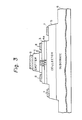
- Fig. 3 is a cross-sectional view of an HET according to an embodiment of the present invention.
- reference numerals 1, 2, 3, and 5 represent an emitter layer, an emitter potential barrier layer, a base layer, and a collector layer, respectively.
- a new collector potential barrier layer 4a is further provided.
- the collector layer 5 is formed on a semiinsulating GaAs substrate 6, the collector-potential barrier (CPB) layer 4a is formed on the collector layer 5, the base layer 3 is formed on the CPB 4a, and the emitter-potential barrier (EPB) layer 2 is formed on the base layer 3.
- the emitter layer 1 is formed on the emitter-potential barrier layer 2, and a collector electrode 7 made of gold germanium/ gold (Au Ge/Au) is formed on the collector layer 5 so as to be in ohmic contact with the collector layer 5.
- the notation Au ⁇ Ge/Au represents a state wherein an alloy Au ⁇ Ge is covered by a layer of Au.
- a base electrode 8 made of gold ⁇ germanium/ gold (Au Ge/Au) is formed on the base layer 3 so as to be in ohmic contact with the base layer 3.
- the term Au ⁇ Ge/Au represents a state wherein an alloy Au ⁇ Ge is covered by a layer ofAu.
- An emitter electrode 9 made of gold germanium/gold (Au Ge/Au) is formed on the emitter layer 1 so as to be in ohmic contact with the emitter layer 1. Examples of the combination of the material in the embodiment shown in Fig. 3 are as follows.
- Fig. 4A is an energy band diagram in a thermal equilibrium state of the HET of the embodiment shown in Fig. 3.
- the conduction band in the collector-potential barrier layer 4a in this embodiment has a structure having a barrier height changing from a high level to a low level along the direction from the base layer 3 to the collector layer 5. That is, the barrier height between the base layer 3 and the collector potential barrier layer4a is BH 1 , which is as high as, for example, 0.30 eV.
- the barrier height BH may or may not be the same as the barrier height of the emitter potential barrier layer 2.
- the barrier height BH 1 is shown as being lower than the barrier height of the emitter potential barrier layer 2.
- the barrier height between the collector potential barrier layer 4a and the collector layer 5 is BH 2 , which is a value smaller than the potential barrier of the emitter potential barrier layer 2 and higher than the lowest energy level E cc of the conduction band in the collector layer 5.
- the potential barrier in the layer 4a is for example linearly decreased from BH 1 to BH 2 .
- the value x at the intrinsic type Al x Ga 1-x As collector potential barrier layer 4a is reduced from the base layer 3 side to the collector layer 5 side, whereby a grading state is achieved. By doing so, the potential barrier also falls, as illustrated.
- Fig. 4B is an energy band diagram illustrating in an operating state of the HET according to an embodiment of the present invention.
- a positive bias voltage V BE is applied between the base layer 3 and the emitter layer 1 so that the base Fermi level E FB is lowered by, for example, 0.30 eV, from the emitter Fermi level E FE .
- the lowest energy level E CB of the base conduction band is also lowered by 0.3 eV from the energy level E CE .
- no voltage is applied between the collector layer 5 and the emitter layer 1. Therefore, the lowest energy level E CE of the conduction band of the emitter layer 1 is the same as the lowest energy level E CE of the conduction band of the collector layer 5.
- the collector potential barrier layer 4a is lowered to be lower than the lowest energy level E cc of the collector conduction band.
- Each of the electrons e tunneling from the emitter layer 1 through the emitter potential barrier layer 2 to the base layer 3 has a kinetic energy higher than the energy level E CE or E cc . Since the collector potential barrier layer 4a does not act as a potential barrier for the electrons having the energy higher than E cc or E CE' the hot electrons in the base layer 3 will easily cross the collector potential barrier layer 4 and reach the collector layer 5.
- the collector potential barrier layer 4a in Fig. 4B does not act as a potential barrier but acts as a PN junction, such as that in a conventional bipolar transistor, for insulating the base layer 3 from the collector layer 5.
- the barrier height BH 2 at the collector layer 5 side is determined to be as small as possible as long as electrons in the collector layer 5 do not enter the base layer 3 due to thermal diffusion.
- the barrier height BH 1 of the base layer 3 side at the collector side potential barrier layer 4a may be 0.3 eV and the barrier height BH 2 of the collector layer 5 side may be 0.1 to 0.2 eV.
- Fig. 5 is a graph showing the relationship between the collector emitter voltage V cE and the collector current l c according to an embodiment of the present invention in the state as shown in Fig. 4B.
- the horizontal axis indicates the collector emitter voltage V CE and the vertical axis the collector current I c .
- a collector current l c begins to flow even when the collector emitter voltage V CE is almost zero. Further, even if the base emitter voltage V BE is made high, there is almost no shifting of the lowest collector emitter voltage V cE for conducting a collector current I c . Therefore, the switching speed can be improved and the power consumption reduced.
- the low output L shown in Fig. 5 is sufficiently low in comparison with the low output shown in Fig. 2. Therefore, the HET according to the embodiment of the present invention is convenient for use in a logic circuit, since no level shift circuit is necessary.
- the content of AI in the crystalline layer may be gradually changed or the MBE method may be applied to form superimposed films of intrinsic type Al x Ga 1-x As with different x values.
- withstand voltage when the collector layer is made positive in potential, should be more than the power supply voltage at the circuit. When made negative in potential, however, it may be about the same as the withstand voltage between the base and emitter. Therefore, the problem of withstand voltage is not an immediate concern.
- Fig. 6A and 6B show another embodiment of the present invention.
- another (alternative) emitter potential barrier layer 2a is employed in this embodiment.
- the emitter potential barrier layer 2a has at least one quantum well QW known as a superlattice.
- the quantum well QW is made of, for example, GaAs.
- Both emitter barrier layers 2a, and 2a 2 adjacent to the quantum well QW are made of Al x Ga 1-x As, where x is a value equal to 0.33.
- the value x in the layers 2a, and 2a z should be greater than a value y in Al y G 1-y As in the collector potential barrier layer 4a.
- Resonant tunneling through such a quantum well QW itself is a known phenomenon, described in, for example, "Resonant tunneling through quantum wells at frequencies up to 2.5 THz", by T. C. L. G. Sollner, et al., Appl. Phys. Lett. 43 (6), 15 September 1983 pp. 588-590.
- the superlattice structure is applied to the emitter potential barrier layer 2a.
- the operation of a resonant hot electron transistor employing the graded collector potential barrier layer 4a is very similar to the operation as described with reference to Fig. 4B. Therefore, the description for operation with reference to Fig. 6B is omitted here.
- the barrier height at the collector potential barrier layer is gradually reduced from the base layer side to the collector layer side, so even when almost no collector emitter voltage is applied, electrons tunneling from the emitter layer through the emitter potential barrier for injection into the base layer will be able to cross the collector side potential barrier layer and reach the collector layer without any hindrance.
Landscapes
- Engineering & Computer Science (AREA)
- Chemical & Material Sciences (AREA)
- Nanotechnology (AREA)
- Physics & Mathematics (AREA)
- Mathematical Physics (AREA)
- Theoretical Computer Science (AREA)
- Crystallography & Structural Chemistry (AREA)
- Bipolar Transistors (AREA)
Claims (4)
caractérisé en ce que ladite couche de barrière de potentiel d'émetteur possède une hauteur de barrière constante lorsque le dispositif est en équilibre thermique et en ce que le niveau haut de la hauteur de barrière de ladite couche de barrière de potentiel de collecteur est inférieur à l'énergie cinétique des électrons chauds qui traversent par effet tunnel la couche de barrière de potentiel d'émetteur, de ladite couche d'émetteur vers ladite couche de base, lorsqu'une tension de polarisation de potentiel est appliquée entre ladite couche de base et ladite couche d'émetteur, même lorsque la tension collecteur-émetteur est proche de zéro.
Applications Claiming Priority (2)
| Application Number | Priority Date | Filing Date | Title |
|---|---|---|---|
| JP59242412A JPS61121358A (ja) | 1984-11-19 | 1984-11-19 | 高速半導体装置 |
| JP242412/84 | 1984-11-19 |
Publications (2)
| Publication Number | Publication Date |
|---|---|
| EP0186301A1 EP0186301A1 (fr) | 1986-07-02 |
| EP0186301B1 true EP0186301B1 (fr) | 1990-01-31 |
Family
ID=17088741
Family Applications (1)
| Application Number | Title | Priority Date | Filing Date |
|---|---|---|---|
| EP85308371A Expired - Lifetime EP0186301B1 (fr) | 1984-11-19 | 1985-11-18 | Dispositif semi-conducteur à grande vitesse |
Country Status (4)
| Country | Link |
|---|---|
| EP (1) | EP0186301B1 (fr) |
| JP (1) | JPS61121358A (fr) |
| KR (1) | KR920002670B1 (fr) |
| DE (1) | DE3575814D1 (fr) |
Families Citing this family (7)
| Publication number | Priority date | Publication date | Assignee | Title |
|---|---|---|---|---|
| JPS6158268A (ja) * | 1984-08-30 | 1986-03-25 | Fujitsu Ltd | 高速半導体装置 |
| US4691215A (en) * | 1985-01-09 | 1987-09-01 | American Telephone And Telegraph Company | Hot electron unipolar transistor with two-dimensional degenerate electron gas base with continuously graded composition compound emitter |
| US4912539A (en) * | 1988-08-05 | 1990-03-27 | The University Of Michigan | Narrow-band-gap base transistor structure with dual collector-base barrier including a graded barrier |
| JPH02210878A (ja) * | 1989-02-10 | 1990-08-22 | Yokogawa Electric Corp | ホットエレクトロントランジスタ |
| JP2731089B2 (ja) * | 1991-10-02 | 1998-03-25 | 三菱電機株式会社 | 高速動作半導体装置およびその製造方法 |
| KR0170181B1 (ko) * | 1994-12-19 | 1999-02-01 | 정선종 | 공진 터널링 핫 전자 트랜지스터 |
| DE19824111A1 (de) * | 1998-05-29 | 1999-12-02 | Daimler Chrysler Ag | Resonanz Phasen Transistor mit gegenphasiger Ladungsträgerinjektion |
Family Cites Families (1)
| Publication number | Priority date | Publication date | Assignee | Title |
|---|---|---|---|---|
| US4353081A (en) * | 1980-01-29 | 1982-10-05 | Bell Telephone Laboratories, Incorporated | Graded bandgap rectifying semiconductor devices |
-
1984
- 1984-11-19 JP JP59242412A patent/JPS61121358A/ja active Granted
-
1985
- 1985-11-18 EP EP85308371A patent/EP0186301B1/fr not_active Expired - Lifetime
- 1985-11-18 DE DE8585308371T patent/DE3575814D1/de not_active Expired - Lifetime
- 1985-11-18 KR KR1019850008603A patent/KR920002670B1/ko not_active Expired
Also Published As
| Publication number | Publication date |
|---|---|
| DE3575814D1 (de) | 1990-03-08 |
| JPS61121358A (ja) | 1986-06-09 |
| EP0186301A1 (fr) | 1986-07-02 |
| KR920002670B1 (ko) | 1992-03-31 |
| JPH0458707B2 (fr) | 1992-09-18 |
| KR860004468A (ko) | 1986-06-23 |
Similar Documents
| Publication | Publication Date | Title |
|---|---|---|
| US4958201A (en) | Resonant tunneling minority carrier transistor | |
| US5389804A (en) | Resonant-tunneling heterojunction bipolar transistor device | |
| EP0133342B1 (fr) | Structure de semi-conducteur avec supraréseau à haute densité de porteurs de charge | |
| US4912531A (en) | Three-terminal quantum device | |
| KR19980034078A (ko) | 핫 전자 장치(Hot Electron Device) 및 공진 터널링 핫 전자 장치 | |
| US5811844A (en) | Low noise, high power pseudomorphic HEMT | |
| JPH02231777A (ja) | 共鳴トンネル光電素子 | |
| US5932889A (en) | Semiconductor device with floating quantum box | |
| EP0279587B1 (fr) | Circuit comparateur | |
| US4768074A (en) | Heterojunction bipolar transistor having an emitter region with a band gap greater than that of a base region | |
| EP0186301B1 (fr) | Dispositif semi-conducteur à grande vitesse | |
| KR920006434B1 (ko) | 공진 터널링 장벽구조장치 | |
| JPH05190834A (ja) | 高速動作半導体装置およびその製造方法 | |
| US5543749A (en) | Resonant tunneling transistor | |
| US5532486A (en) | Heterojunction diode with low turn-on voltage | |
| US4645707A (en) | Semiconductor devices | |
| US4670767A (en) | Hetero-junction bipolar transistor having a high switching speed | |
| EP0268512A2 (fr) | Dispositif semi-conducteur à effet de tunnel résonnant | |
| EP0216155A2 (fr) | Dispositif à effet-tunnel avec trois pôles | |
| US5214297A (en) | High-speed semiconductor device | |
| US4916495A (en) | Semiconductor device with semi-metal | |
| US5021863A (en) | Semiconductor quantum effect device having negative differential resistance characteristics | |
| US6031245A (en) | Semiconductor device | |
| US5895931A (en) | Semiconductor device | |
| KR100222398B1 (ko) | 공진 터널링 전자 장치 |
Legal Events
| Date | Code | Title | Description |
|---|---|---|---|
| PUAI | Public reference made under article 153(3) epc to a published international application that has entered the european phase |
Free format text: ORIGINAL CODE: 0009012 |
|
| AK | Designated contracting states |
Kind code of ref document: A1 Designated state(s): DE FR GB |
|
| 17P | Request for examination filed |
Effective date: 19860924 |
|
| 17Q | First examination report despatched |
Effective date: 19880614 |
|
| GRAA | (expected) grant |
Free format text: ORIGINAL CODE: 0009210 |
|
| AK | Designated contracting states |
Kind code of ref document: B1 Designated state(s): DE FR GB |
|
| REF | Corresponds to: |
Ref document number: 3575814 Country of ref document: DE Date of ref document: 19900308 |
|
| ET | Fr: translation filed | ||
| PLBE | No opposition filed within time limit |
Free format text: ORIGINAL CODE: 0009261 |
|
| STAA | Information on the status of an ep patent application or granted ep patent |
Free format text: STATUS: NO OPPOSITION FILED WITHIN TIME LIMIT |
|
| 26N | No opposition filed | ||
| PGFP | Annual fee paid to national office [announced via postgrant information from national office to epo] |
Ref country code: FR Payment date: 19921127 Year of fee payment: 8 |
|
| PGFP | Annual fee paid to national office [announced via postgrant information from national office to epo] |
Ref country code: DE Payment date: 19930129 Year of fee payment: 8 |
|
| PG25 | Lapsed in a contracting state [announced via postgrant information from national office to epo] |
Ref country code: FR Effective date: 19940729 |
|
| PG25 | Lapsed in a contracting state [announced via postgrant information from national office to epo] |
Ref country code: DE Effective date: 19940802 |
|
| REG | Reference to a national code |
Ref country code: FR Ref legal event code: ST |
|
| PGFP | Annual fee paid to national office [announced via postgrant information from national office to epo] |
Ref country code: GB Payment date: 19951109 Year of fee payment: 11 |
|
| PG25 | Lapsed in a contracting state [announced via postgrant information from national office to epo] |
Ref country code: GB Effective date: 19961118 |
|
| GBPC | Gb: european patent ceased through non-payment of renewal fee |
Effective date: 19961118 |