EP0201686A1 - Dispositif semi-conducteur comprenant un super-réseau - Google Patents
Dispositif semi-conducteur comprenant un super-réseau Download PDFInfo
- Publication number
- EP0201686A1 EP0201686A1 EP86103408A EP86103408A EP0201686A1 EP 0201686 A1 EP0201686 A1 EP 0201686A1 EP 86103408 A EP86103408 A EP 86103408A EP 86103408 A EP86103408 A EP 86103408A EP 0201686 A1 EP0201686 A1 EP 0201686A1
- Authority
- EP
- European Patent Office
- Prior art keywords
- layer
- semiconductor
- electron
- phonon
- gaas
- Prior art date
- Legal status (The legal status is an assumption and is not a legal conclusion. Google has not performed a legal analysis and makes no representation as to the accuracy of the status listed.)
- Granted
Links
Images


Classifications
-
- H—ELECTRICITY
- H10—SEMICONDUCTOR DEVICES; ELECTRIC SOLID-STATE DEVICES NOT OTHERWISE PROVIDED FOR
- H10D—INORGANIC ELECTRIC SEMICONDUCTOR DEVICES
- H10D62/00—Semiconductor bodies, or regions thereof, of devices having potential barriers
- H10D62/80—Semiconductor bodies, or regions thereof, of devices having potential barriers characterised by the materials
- H10D62/81—Semiconductor bodies, or regions thereof, of devices having potential barriers characterised by the materials of structures exhibiting quantum-confinement effects, e.g. single quantum wells; of structures having periodic or quasi-periodic potential variation
- H10D62/815—Semiconductor bodies, or regions thereof, of devices having potential barriers characterised by the materials of structures exhibiting quantum-confinement effects, e.g. single quantum wells; of structures having periodic or quasi-periodic potential variation of structures having periodic or quasi-periodic potential variation, e.g. superlattices or multiple quantum wells [MQW]
- H10D62/8161—Semiconductor bodies, or regions thereof, of devices having potential barriers characterised by the materials of structures exhibiting quantum-confinement effects, e.g. single quantum wells; of structures having periodic or quasi-periodic potential variation of structures having periodic or quasi-periodic potential variation, e.g. superlattices or multiple quantum wells [MQW] potential variation due to variations in composition or crystallinity, e.g. heterojunction superlattices
- H10D62/8162—Semiconductor bodies, or regions thereof, of devices having potential barriers characterised by the materials of structures exhibiting quantum-confinement effects, e.g. single quantum wells; of structures having periodic or quasi-periodic potential variation of structures having periodic or quasi-periodic potential variation, e.g. superlattices or multiple quantum wells [MQW] potential variation due to variations in composition or crystallinity, e.g. heterojunction superlattices having quantum effects only in the vertical direction, i.e. layered structures having quantum effects solely resulting from vertical potential variation
- H10D62/8164—Semiconductor bodies, or regions thereof, of devices having potential barriers characterised by the materials of structures exhibiting quantum-confinement effects, e.g. single quantum wells; of structures having periodic or quasi-periodic potential variation of structures having periodic or quasi-periodic potential variation, e.g. superlattices or multiple quantum wells [MQW] potential variation due to variations in composition or crystallinity, e.g. heterojunction superlattices having quantum effects only in the vertical direction, i.e. layered structures having quantum effects solely resulting from vertical potential variation comprising only semiconductor materials
-
- H—ELECTRICITY
- H10—SEMICONDUCTOR DEVICES; ELECTRIC SOLID-STATE DEVICES NOT OTHERWISE PROVIDED FOR
- H10D—INORGANIC ELECTRIC SEMICONDUCTOR DEVICES
- H10D10/00—Bipolar junction transistors [BJT]
- H10D10/80—Heterojunction BJTs
- H10D10/821—Vertical heterojunction BJTs
- H10D10/881—Resonant tunnelling transistors
-
- Y—GENERAL TAGGING OF NEW TECHNOLOGICAL DEVELOPMENTS; GENERAL TAGGING OF CROSS-SECTIONAL TECHNOLOGIES SPANNING OVER SEVERAL SECTIONS OF THE IPC; TECHNICAL SUBJECTS COVERED BY FORMER USPC CROSS-REFERENCE ART COLLECTIONS [XRACs] AND DIGESTS
- Y10—TECHNICAL SUBJECTS COVERED BY FORMER USPC
- Y10S—TECHNICAL SUBJECTS COVERED BY FORMER USPC CROSS-REFERENCE ART COLLECTIONS [XRACs] AND DIGESTS
- Y10S148/00—Metal treatment
- Y10S148/011—Bipolar transistors
-
- Y—GENERAL TAGGING OF NEW TECHNOLOGICAL DEVELOPMENTS; GENERAL TAGGING OF CROSS-SECTIONAL TECHNOLOGIES SPANNING OVER SEVERAL SECTIONS OF THE IPC; TECHNICAL SUBJECTS COVERED BY FORMER USPC CROSS-REFERENCE ART COLLECTIONS [XRACs] AND DIGESTS
- Y10—TECHNICAL SUBJECTS COVERED BY FORMER USPC
- Y10S—TECHNICAL SUBJECTS COVERED BY FORMER USPC CROSS-REFERENCE ART COLLECTIONS [XRACs] AND DIGESTS
- Y10S148/00—Metal treatment
- Y10S148/056—Gallium arsenide
-
- Y—GENERAL TAGGING OF NEW TECHNOLOGICAL DEVELOPMENTS; GENERAL TAGGING OF CROSS-SECTIONAL TECHNOLOGIES SPANNING OVER SEVERAL SECTIONS OF THE IPC; TECHNICAL SUBJECTS COVERED BY FORMER USPC CROSS-REFERENCE ART COLLECTIONS [XRACs] AND DIGESTS
- Y10—TECHNICAL SUBJECTS COVERED BY FORMER USPC
- Y10S—TECHNICAL SUBJECTS COVERED BY FORMER USPC CROSS-REFERENCE ART COLLECTIONS [XRACs] AND DIGESTS
- Y10S148/00—Metal treatment
- Y10S148/072—Heterojunctions
-
- Y—GENERAL TAGGING OF NEW TECHNOLOGICAL DEVELOPMENTS; GENERAL TAGGING OF CROSS-SECTIONAL TECHNOLOGIES SPANNING OVER SEVERAL SECTIONS OF THE IPC; TECHNICAL SUBJECTS COVERED BY FORMER USPC CROSS-REFERENCE ART COLLECTIONS [XRACs] AND DIGESTS
- Y10—TECHNICAL SUBJECTS COVERED BY FORMER USPC
- Y10S—TECHNICAL SUBJECTS COVERED BY FORMER USPC CROSS-REFERENCE ART COLLECTIONS [XRACs] AND DIGESTS
- Y10S148/00—Metal treatment
- Y10S148/097—Lattice strain and defects
-
- Y—GENERAL TAGGING OF NEW TECHNOLOGICAL DEVELOPMENTS; GENERAL TAGGING OF CROSS-SECTIONAL TECHNOLOGIES SPANNING OVER SEVERAL SECTIONS OF THE IPC; TECHNICAL SUBJECTS COVERED BY FORMER USPC CROSS-REFERENCE ART COLLECTIONS [XRACs] AND DIGESTS
- Y10—TECHNICAL SUBJECTS COVERED BY FORMER USPC
- Y10S—TECHNICAL SUBJECTS COVERED BY FORMER USPC CROSS-REFERENCE ART COLLECTIONS [XRACs] AND DIGESTS
- Y10S148/00—Metal treatment
- Y10S148/119—Phosphides of gallium or indium
-
- Y—GENERAL TAGGING OF NEW TECHNOLOGICAL DEVELOPMENTS; GENERAL TAGGING OF CROSS-SECTIONAL TECHNOLOGIES SPANNING OVER SEVERAL SECTIONS OF THE IPC; TECHNICAL SUBJECTS COVERED BY FORMER USPC CROSS-REFERENCE ART COLLECTIONS [XRACs] AND DIGESTS
- Y10—TECHNICAL SUBJECTS COVERED BY FORMER USPC
- Y10S—TECHNICAL SUBJECTS COVERED BY FORMER USPC CROSS-REFERENCE ART COLLECTIONS [XRACs] AND DIGESTS
- Y10S148/00—Metal treatment
- Y10S148/16—Superlattice
Definitions
- the present invention relates to a semiconductor apparatus suitable for being applied to semiconductor electron elements, such as various kinds of a field effect transistor (FET), a hot electron transistor (HET), a heterojunction type bipolar transistor (HBT) and so on.
- semiconductor electron elements such as various kinds of a field effect transistor (FET), a hot electron transistor (HET), a heterojunction type bipolar transistor (HBT) and so on.
- FET field effect transistor
- HET hot electron transistor
- HBT heterojunction type bipolar transistor
- the electron mobility near the room temperature is determined in practice by the electron scattering caused by LO phonon. Therefore, there is a problem that it is not expected to realize an adequately high electron mobility.
- An object of the present invention is to provide an improved semiconductor apparatus.
- Another object of the present invention is to obtain the modulation effect of the electron mobility and to provide various semiconductor apparatus by utilizing this effect.
- This invention is, in a semiconductor heterostructure superlattice in which a plurality of different thin semiconductors of less than 8 monolayers are repeatedly laminated, particularly when each of semiconductor layers is made of single atom or low atom, to obtain a special property, that is, an effect of de-localized state of the electron or localized state of the LO phonon (longitudinal optical phonon) with respect to the laminated layer direction in each semiconductor layer and then to find out that the electron mobility can be modulated by the mutual action therebetween.
- the whole or apart of the electron active region of various semiconductor electron apparatus is formed by the superlattice of the ultrathin semiconductor substance having a low atomic layer and a main electron active direction is selected to be in the laminated layer direction of this semiconductor layer.
- the present invention is, in a semiconductor heterostructure superlattice having a periodic structure in which a plurality of different semiconductor layers are repeatedly laminated, based on such a search that when the semiconductor layer is formed as a ultrathin layer, i.e., a thin layer having a thickness less than 8 monolayers, it exhibits such a property which is different from Kronig-Penney electron model, the electrons are delocalized and LO phonon can be localized.
- a semiconductor layer 2 having a superlattice structure such that a plurality of different semiconductor layers L 1 , L 2 , L 3 , ... L n made of less than 8 monolayers each containing a fraction or binary compound semiconductor and which are alternately and repeatedly laminated with a plurality of periodic layer numbers M are epitaxially grown by the MOCVD (Metal Organic Chemical Vapour Deposition) method or NBE (Molecular Beam Epitaxy) method, whereby the whole or part of electron active region is constructed.
- MOCVD Metal Organic Chemical Vapour Deposition
- NBE Molecular Beam Epitaxy
- a broken line curve indicates the energy gaps that are provided by the calculation based on the Kronig-Penney electron model theory.
- n ⁇ 8 they do not coincide with thcse in the kronig-Penney electron model.
- Raman scattering experiment was carried out. The measurement was carried out by using an excitation light having a wavelength of 514.
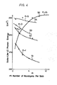
- Fig. 3 shows measured results of the dependence of GaAs-like LO phonon energy in the (AlAs)m (GaAs)n on n.
- the GaAs-like LO phonon energy is determined by not the value of m but the value of n, that is, the GaAs monolayer.
- the respective curves 51 to 54 each taking n as a parameter, although the GaAs-like LO phonon energy is varied considerably as n is varied, the respective curves 51 to 54 present gentle inclinations. In other words, they have small dependence on the value m.
- FIG. 5 shows measured results of the dependence of AlAs-like LO phonons energy in the (AlAs)m (GaAs)n on m.
- the energy of the AlAs-like LO phonon is determined by not the value n but the value m, that is, the AlAs monolayer.
- Fig. 6 shows measured results of the dependence of AlAs-like LO phonon on the value n. In Fig.
- the GaAs-like phonon energy is not dependent on the number m of the AlAs monolayers but is determined by the number n of the GaAs monolayers
- the AlAs-like phonon energy is not dependent on the number n of the GaAs monolayers but is determined by the number m of the AlAs monolayers.
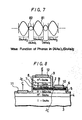
- the LO phonons are localized in the GaAs layer and the AlAs layer, respectively. That is, as, for example, shown by wave functions in (AlAs) 1 (GaAs) 2 in Fig. 7, respective wave functions of the GaAs-like phonon and AlAs-like phonon are standing waves which are localized in the GaAs layer and the AlAs layer as shown by curves 81 and 82, respectively.
- the GaAs-like phonon and the AlAs-like phonon are respectively localized and kinetic momenta thereof are modulated by the values n and m, respectively.
- the LO phonon is localized by the superlattice structure having less than 8 monolayers and the kinetic momentum thereof is modulated, accordingly, the scattering probability concerning the electron is modulated, whereby it is possible to realize the high speed semiconductor apparatus and the like.
- 2 ⁇ (Ef - Ei) (1) (h h/2 and h is the planck's constant) M L0-e is proportionate to the reciprocal number of momentum.
- MLD-e in aforesaid superlattice is smaller than that in bulk. Accordingly, the scattering probability of the electron by the LO phonon becomes very small so that the modulation of the electron mobility occurs.
- an npn-type HBT is formed.
- an n-type GaAs collector electrode deriving layer 4 having a low resistivity on which a collector layer 5 of, for example, an n-type AlGaAs semiconductor layer having a large band-gap, which forms a collector pn junction Jc of a hetero type between it and a base layer 6 which will be mentioned later, is epitaxially grown.
- an epitaxial layer 7 made of an n type AlGaAs having a large band-gap is formed on this layer.
- n type GaAs semiconductor layer 8 there is epitaxially grown, for example, n type GaAs semiconductor layer 8 to thereby form an emitter junction J E of a heterojunction type by the pn junction, between the emitter layer 7 and the base layer 6.
- an emitter electrode deriving layer 9 made of, for example, an n-type GaAs semiconductor layer having a low resistivity.
- Parts of the semiconductor layers 9, 8 and 7 are removed by etching to expose a part of the base layer 6 on which a base electrode is deposited in ohmio contact. Further, parts of the semiconductor layers 9, 8, 7 and 6 are removed by etching to expose to the outside a part of the collector electrode deriving layer 4 on which a collector electrode 11 is deposited in ohmic contact and an emitter electrode 12 is deposited on the emitter electrode deriving region 9 in ohmic contact.
- the HBT having the structure thus made comprises the base layer 6 which has the above mentioned superlattice structure having less than 8 atomic layers and the longitudinal structure in which the electron active direction is selected to be in the layer laminated direction of. the superlattice structure so that the electron mobility can be set as a high one as described before.
- the switching speed can be increased and also the transport efficiency can be increased.
- the LO phonon can be localized, it is possible to carry out the modulation of the electron mobility that can not be expected in the prior art. As a result, it is possible to obtain various semiconductor apparatus having excellent characteristics that can not be presented in the prior art.
Landscapes
- Bipolar Transistors (AREA)
- Junction Field-Effect Transistors (AREA)
Applications Claiming Priority (2)
| Application Number | Priority Date | Filing Date | Title |
|---|---|---|---|
| JP52973/85 | 1985-03-15 | ||
| JP60052973A JPS61210679A (ja) | 1985-03-15 | 1985-03-15 | 半導体装置 |
Publications (2)
| Publication Number | Publication Date |
|---|---|
| EP0201686A1 true EP0201686A1 (fr) | 1986-11-20 |
| EP0201686B1 EP0201686B1 (fr) | 1991-02-20 |
Family
ID=12929834
Family Applications (1)
| Application Number | Title | Priority Date | Filing Date |
|---|---|---|---|
| EP86103408A Expired EP0201686B1 (fr) | 1985-03-15 | 1986-03-13 | Dispositif semi-conducteur comprenant un super-réseau |
Country Status (4)
| Country | Link |
|---|---|
| US (2) | US4835579A (fr) |
| EP (1) | EP0201686B1 (fr) |
| JP (1) | JPS61210679A (fr) |
| DE (1) | DE3677543D1 (fr) |
Cited By (6)
| Publication number | Priority date | Publication date | Assignee | Title |
|---|---|---|---|---|
| EP0238406A3 (en) * | 1986-03-13 | 1987-11-19 | Fujitsu Limited | Heterojunction semiconductor device |
| FR2607628A1 (fr) * | 1986-11-27 | 1988-06-03 | Centre Nat Rech Scient | Modulateur optique a superreseau |
| EP0292568A4 (fr) * | 1986-12-03 | 1989-04-12 | Hitachi Ltd | Transistor bipolaire a heterojonction. |
| US5129831A (en) * | 1991-07-26 | 1992-07-14 | Amp Incorporated | Right angle header shroud to board polarization and keying system |
| US5161996A (en) * | 1991-07-26 | 1992-11-10 | Amp Incorporated | Header assembly and alignment assist shroud therefor |
| NL1023764C2 (nl) | 2003-06-27 | 2004-12-28 | Leen Huisman B V | Insectwerend schermdoek en scherminrichting. |
Families Citing this family (167)
| Publication number | Priority date | Publication date | Assignee | Title |
|---|---|---|---|---|
| JPS624366A (ja) * | 1985-07-01 | 1987-01-10 | Fujitsu Ltd | ホツトエレクトロントランジスタ |
| JPS62166564A (ja) * | 1986-01-20 | 1987-07-23 | Agency Of Ind Science & Technol | 半導体装置 |
| US5258631A (en) * | 1987-01-30 | 1993-11-02 | Hitachi, Ltd. | Semiconductor device having a two-dimensional electron gas as an active layer |
| US4956682A (en) * | 1987-04-28 | 1990-09-11 | Matsushita Electric Industrial Co., Ltd. | Optoelectronic integrated circuit |
| FR2620863B1 (fr) * | 1987-09-22 | 1989-12-01 | Thomson Csf | Dispositif optoelectronique a base de composes iii-v sur substrat silicium |
| US5381027A (en) * | 1988-01-26 | 1995-01-10 | Hitachi, Ltd. | Semiconductor device having a heterojunction and a two dimensional gas as an active layer |
| JPH01238161A (ja) * | 1988-03-18 | 1989-09-22 | Fujitsu Ltd | 半導体装置及びその製造方法 |
| US4905056A (en) * | 1988-09-30 | 1990-02-27 | Berndt Dale F | Superlattice precision voltage reference |
| JPH06101588B2 (ja) * | 1989-08-22 | 1994-12-12 | 京都大学長 | 半導体材料 |
| JPH03290975A (ja) * | 1990-04-09 | 1991-12-20 | Fujitsu Ltd | 縦型半導体装置 |
| US5087948A (en) * | 1990-06-25 | 1992-02-11 | Massachusetts Institute Of Technology | Disorder-induced narrowband high-speed electronic devices |
| US5160982A (en) * | 1991-07-01 | 1992-11-03 | Motorola, Inc. | Phonon suppression in quantum wells |
| US5426316A (en) * | 1992-12-21 | 1995-06-20 | International Business Machines Corporation | Triple heterojunction bipolar transistor |
| JPH0786184A (ja) * | 1993-09-20 | 1995-03-31 | Nec Kansai Ltd | 結晶成長方法 |
| US5773334A (en) * | 1994-09-26 | 1998-06-30 | Toyota Jidosha Kabushiki Kaisha | Method of manufacturing a semiconductor device |
| US6320212B1 (en) * | 1999-09-02 | 2001-11-20 | Hrl Laboratories, Llc. | Superlattice fabrication for InAs/GaSb/AISb semiconductor structures |
| US20050282330A1 (en) * | 2003-06-26 | 2005-12-22 | Rj Mears, Llc | Method for making a semiconductor device including a superlattice having at least one group of substantially undoped layers |
| US7033437B2 (en) * | 2003-06-26 | 2006-04-25 | Rj Mears, Llc | Method for making semiconductor device including band-engineered superlattice |
| US20070015344A1 (en) * | 2003-06-26 | 2007-01-18 | Rj Mears, Llc | Method for Making a Semiconductor Device Including a Strained Superlattice Between at Least One Pair of Spaced Apart Stress Regions |
| US20060289049A1 (en) * | 2003-06-26 | 2006-12-28 | Rj Mears, Llc | Semiconductor Device Having a Semiconductor-on-Insulator (SOI) Configuration and Including a Superlattice on a Thin Semiconductor Layer |
| US7612366B2 (en) * | 2003-06-26 | 2009-11-03 | Mears Technologies, Inc. | Semiconductor device including a strained superlattice layer above a stress layer |
| US7598515B2 (en) * | 2003-06-26 | 2009-10-06 | Mears Technologies, Inc. | Semiconductor device including a strained superlattice and overlying stress layer and related methods |
| US7153763B2 (en) | 2003-06-26 | 2006-12-26 | Rj Mears, Llc | Method for making a semiconductor device including band-engineered superlattice using intermediate annealing |
| US7514328B2 (en) * | 2003-06-26 | 2009-04-07 | Mears Technologies, Inc. | Method for making a semiconductor device including shallow trench isolation (STI) regions with a superlattice therebetween |
| US20060220118A1 (en) * | 2003-06-26 | 2006-10-05 | Rj Mears, Llc | Semiconductor device including a dopant blocking superlattice |
| US7531828B2 (en) * | 2003-06-26 | 2009-05-12 | Mears Technologies, Inc. | Semiconductor device including a strained superlattice between at least one pair of spaced apart stress regions |
| US7531850B2 (en) * | 2003-06-26 | 2009-05-12 | Mears Technologies, Inc. | Semiconductor device including a memory cell with a negative differential resistance (NDR) device |
| US20040262594A1 (en) * | 2003-06-26 | 2004-12-30 | Rj Mears, Llc | Semiconductor structures having improved conductivity effective mass and methods for fabricating same |
| US7227174B2 (en) * | 2003-06-26 | 2007-06-05 | Rj Mears, Llc | Semiconductor device including a superlattice and adjacent semiconductor layer with doped regions defining a semiconductor junction |
| US7659539B2 (en) | 2003-06-26 | 2010-02-09 | Mears Technologies, Inc. | Semiconductor device including a floating gate memory cell with a superlattice channel |
| US7202494B2 (en) * | 2003-06-26 | 2007-04-10 | Rj Mears, Llc | FINFET including a superlattice |
| US7531829B2 (en) | 2003-06-26 | 2009-05-12 | Mears Technologies, Inc. | Semiconductor device including regions of band-engineered semiconductor superlattice to reduce device-on resistance |
| US7045377B2 (en) * | 2003-06-26 | 2006-05-16 | Rj Mears, Llc | Method for making a semiconductor device including a superlattice and adjacent semiconductor layer with doped regions defining a semiconductor junction |
| US7535041B2 (en) * | 2003-06-26 | 2009-05-19 | Mears Technologies, Inc. | Method for making a semiconductor device including regions of band-engineered semiconductor superlattice to reduce device-on resistance |
| US20050279991A1 (en) * | 2003-06-26 | 2005-12-22 | Rj Mears, Llc | Semiconductor device including a superlattice having at least one group of substantially undoped layers |
| US20070063186A1 (en) * | 2003-06-26 | 2007-03-22 | Rj Mears, Llc | Method for making a semiconductor device including a front side strained superlattice layer and a back side stress layer |
| US7045813B2 (en) * | 2003-06-26 | 2006-05-16 | Rj Mears, Llc | Semiconductor device including a superlattice with regions defining a semiconductor junction |
| US20070020860A1 (en) * | 2003-06-26 | 2007-01-25 | Rj Mears, Llc | Method for Making Semiconductor Device Including a Strained Superlattice and Overlying Stress Layer and Related Methods |
| US6958486B2 (en) * | 2003-06-26 | 2005-10-25 | Rj Mears, Llc | Semiconductor device including band-engineered superlattice |
| US20060267130A1 (en) * | 2003-06-26 | 2006-11-30 | Rj Mears, Llc | Semiconductor Device Including Shallow Trench Isolation (STI) Regions with a Superlattice Therebetween |
| US20060292765A1 (en) * | 2003-06-26 | 2006-12-28 | Rj Mears, Llc | Method for Making a FINFET Including a Superlattice |
| US7491587B2 (en) * | 2003-06-26 | 2009-02-17 | Mears Technologies, Inc. | Method for making a semiconductor device having a semiconductor-on-insulator (SOI) configuration and including a superlattice on a thin semiconductor layer |
| US7586116B2 (en) * | 2003-06-26 | 2009-09-08 | Mears Technologies, Inc. | Semiconductor device having a semiconductor-on-insulator configuration and a superlattice |
| US20060273299A1 (en) * | 2003-06-26 | 2006-12-07 | Rj Mears, Llc | Method for making a semiconductor device including a dopant blocking superlattice |
| US7229902B2 (en) * | 2003-06-26 | 2007-06-12 | Rj Mears, Llc | Method for making a semiconductor device including a superlattice with regions defining a semiconductor junction |
| US20060231857A1 (en) * | 2003-06-26 | 2006-10-19 | Rj Mears, Llc | Method for making a semiconductor device including a memory cell with a negative differential resistance (ndr) device |
| US20070010040A1 (en) * | 2003-06-26 | 2007-01-11 | Rj Mears, Llc | Method for Making a Semiconductor Device Including a Strained Superlattice Layer Above a Stress Layer |
| US20070020833A1 (en) * | 2003-06-26 | 2007-01-25 | Rj Mears, Llc | Method for Making a Semiconductor Device Including a Channel with a Non-Semiconductor Layer Monolayer |
| US20040266116A1 (en) * | 2003-06-26 | 2004-12-30 | Rj Mears, Llc | Methods of fabricating semiconductor structures having improved conductivity effective mass |
| US7586165B2 (en) * | 2003-06-26 | 2009-09-08 | Mears Technologies, Inc. | Microelectromechanical systems (MEMS) device including a superlattice |
| US20070063185A1 (en) * | 2003-06-26 | 2007-03-22 | Rj Mears, Llc | Semiconductor device including a front side strained superlattice layer and a back side stress layer |
| US20060243964A1 (en) * | 2003-06-26 | 2006-11-02 | Rj Mears, Llc | Method for making a semiconductor device having a semiconductor-on-insulator configuration and a superlattice |
| WO2005018005A1 (fr) * | 2003-06-26 | 2005-02-24 | Rj Mears, Llc | Dispositif a semi-conducteur comprenant un transistor mosfet pourvu d'un super-reseau concu sous forme de bande |
| US7446002B2 (en) * | 2003-06-26 | 2008-11-04 | Mears Technologies, Inc. | Method for making a semiconductor device comprising a superlattice dielectric interface layer |
| US20060011905A1 (en) * | 2003-06-26 | 2006-01-19 | Rj Mears, Llc | Semiconductor device comprising a superlattice dielectric interface layer |
| TWM253058U (en) * | 2003-09-05 | 2004-12-11 | Visual Photonics Epitaxy Co Lt | Heterogeneous junction dipole transistor structure for adjusting on voltage of base and emitter |
| US7439555B2 (en) * | 2003-12-05 | 2008-10-21 | International Rectifier Corporation | III-nitride semiconductor device with trench structure |
| TWI316294B (en) * | 2005-12-22 | 2009-10-21 | Mears Technologies Inc | Method for making an electronic device including a selectively polable superlattice |
| US7517702B2 (en) * | 2005-12-22 | 2009-04-14 | Mears Technologies, Inc. | Method for making an electronic device including a poled superlattice having a net electrical dipole moment |
| US7700447B2 (en) * | 2006-02-21 | 2010-04-20 | Mears Technologies, Inc. | Method for making a semiconductor device comprising a lattice matching layer |
| US7781827B2 (en) | 2007-01-24 | 2010-08-24 | Mears Technologies, Inc. | Semiconductor device with a vertical MOSFET including a superlattice and related methods |
| US7928425B2 (en) * | 2007-01-25 | 2011-04-19 | Mears Technologies, Inc. | Semiconductor device including a metal-to-semiconductor superlattice interface layer and related methods |
| US7880161B2 (en) * | 2007-02-16 | 2011-02-01 | Mears Technologies, Inc. | Multiple-wavelength opto-electronic device including a superlattice |
| US7863066B2 (en) * | 2007-02-16 | 2011-01-04 | Mears Technologies, Inc. | Method for making a multiple-wavelength opto-electronic device including a superlattice |
| US7812339B2 (en) * | 2007-04-23 | 2010-10-12 | Mears Technologies, Inc. | Method for making a semiconductor device including shallow trench isolation (STI) regions with maskless superlattice deposition following STI formation and related structures |
| EP2202784B1 (fr) * | 2008-12-29 | 2017-10-25 | Imec | Procédé de fabrication d'une jonction |
| US9099388B2 (en) | 2011-10-21 | 2015-08-04 | Taiwan Semiconductor Manufacturing Company, Ltd. | III-V multi-channel FinFETs |
| CN106104805B (zh) | 2013-11-22 | 2020-06-16 | 阿托梅拉公司 | 包括超晶格穿通停止层堆叠的垂直半导体装置和相关方法 |
| CN105900241B (zh) | 2013-11-22 | 2020-07-24 | 阿托梅拉公司 | 包括超晶格耗尽层堆叠的半导体装置和相关方法 |
| WO2015191561A1 (fr) | 2014-06-09 | 2015-12-17 | Mears Technologies, Inc. | Dispositifs semi-conducteurs à dopage déterministe amélioré et procédés associés |
| US9722046B2 (en) | 2014-11-25 | 2017-08-01 | Atomera Incorporated | Semiconductor device including a superlattice and replacement metal gate structure and related methods |
| CN107810549B (zh) | 2015-05-15 | 2021-12-17 | 阿托梅拉公司 | 具有提供晕圈注入峰值限制的超晶格层的半导体装置和相关方法 |
| US9721790B2 (en) | 2015-06-02 | 2017-08-01 | Atomera Incorporated | Method for making enhanced semiconductor structures in single wafer processing chamber with desired uniformity control |
| US9558939B1 (en) | 2016-01-15 | 2017-01-31 | Atomera Incorporated | Methods for making a semiconductor device including atomic layer structures using N2O as an oxygen source |
| US10109342B2 (en) | 2016-05-11 | 2018-10-23 | Atomera Incorporated | Dram architecture to reduce row activation circuitry power and peripheral leakage and related methods |
| US10170603B2 (en) | 2016-08-08 | 2019-01-01 | Atomera Incorporated | Semiconductor device including a resonant tunneling diode structure with electron mean free path control layers |
| US10107854B2 (en) | 2016-08-17 | 2018-10-23 | Atomera Incorporated | Semiconductor device including threshold voltage measurement circuitry |
| TWI723262B (zh) | 2017-05-16 | 2021-04-01 | 美商安托梅拉公司 | 包含超晶格作為吸除層之半導體元件及方法 |
| US10367064B2 (en) | 2017-06-13 | 2019-07-30 | Atomera Incorporated | Semiconductor device with recessed channel array transistor (RCAT) including a superlattice |
| US10109479B1 (en) | 2017-07-31 | 2018-10-23 | Atomera Incorporated | Method of making a semiconductor device with a buried insulating layer formed by annealing a superlattice |
| CN111247640B (zh) | 2017-08-18 | 2023-11-03 | 阿托梅拉公司 | 包括与超晶格sti界面相邻的非单晶纵梁的半导体器件和方法 |
| US10529757B2 (en) | 2017-12-15 | 2020-01-07 | Atomera Incorporated | CMOS image sensor including pixels with read circuitry having a superlattice |
| US10461118B2 (en) | 2017-12-15 | 2019-10-29 | Atomera Incorporated | Method for making CMOS image sensor including photodiodes with overlying superlattices to reduce crosstalk |
| US10608043B2 (en) | 2017-12-15 | 2020-03-31 | Atomera Incorporation | Method for making CMOS image sensor including stacked semiconductor chips and readout circuitry including a superlattice |
| WO2019118840A1 (fr) | 2017-12-15 | 2019-06-20 | Atomera Incorporated | Capteur d'image cmos comprenant des puces semi-conductrices empilées et un ensemble circuit de lecture comprenant un super-réseau et procédés associés |
| US10367028B2 (en) | 2017-12-15 | 2019-07-30 | Atomera Incorporated | CMOS image sensor including stacked semiconductor chips and image processing circuitry including a superlattice |
| US10355151B2 (en) | 2017-12-15 | 2019-07-16 | Atomera Incorporated | CMOS image sensor including photodiodes with overlying superlattices to reduce crosstalk |
| US10361243B2 (en) | 2017-12-15 | 2019-07-23 | Atomera Incorporated | Method for making CMOS image sensor including superlattice to enhance infrared light absorption |
| US10304881B1 (en) | 2017-12-15 | 2019-05-28 | Atomera Incorporated | CMOS image sensor with buried superlattice layer to reduce crosstalk |
| US10529768B2 (en) | 2017-12-15 | 2020-01-07 | Atomera Incorporated | Method for making CMOS image sensor including pixels with read circuitry having a superlattice |
| US10276625B1 (en) | 2017-12-15 | 2019-04-30 | Atomera Incorporated | CMOS image sensor including superlattice to enhance infrared light absorption |
| US10615209B2 (en) | 2017-12-15 | 2020-04-07 | Atomera Incorporated | CMOS image sensor including stacked semiconductor chips and readout circuitry including a superlattice |
| US10396223B2 (en) | 2017-12-15 | 2019-08-27 | Atomera Incorporated | Method for making CMOS image sensor with buried superlattice layer to reduce crosstalk |
| US10608027B2 (en) | 2017-12-15 | 2020-03-31 | Atomera Incorporated | Method for making CMOS image sensor including stacked semiconductor chips and image processing circuitry including a superlattice |
| WO2019173668A1 (fr) | 2018-03-08 | 2019-09-12 | Atomera Incorporated | Dispositif à semi-conducteur comprenant des structures de contact améliorées comportant un super-réseau et procédés associés |
| US10468245B2 (en) | 2018-03-09 | 2019-11-05 | Atomera Incorporated | Semiconductor device including compound semiconductor materials and an impurity and point defect blocking superlattice |
| CN112005340A (zh) | 2018-03-09 | 2020-11-27 | 阿托梅拉公司 | 包括化合物半导体材料和阻挡杂质和点缺陷的超晶格的半导体器件及方法 |
| US10727049B2 (en) | 2018-03-09 | 2020-07-28 | Atomera Incorporated | Method for making a semiconductor device including compound semiconductor materials and an impurity and point defect blocking superlattice |
| US11664459B2 (en) | 2018-04-12 | 2023-05-30 | Atomera Incorporated | Method for making an inverted T channel field effect transistor (ITFET) including a superlattice |
| US10884185B2 (en) | 2018-04-12 | 2021-01-05 | Atomera Incorporated | Semiconductor device including vertically integrated optical and electronic devices and comprising a superlattice |
| US10811498B2 (en) | 2018-08-30 | 2020-10-20 | Atomera Incorporated | Method for making superlattice structures with reduced defect densities |
| US10566191B1 (en) | 2018-08-30 | 2020-02-18 | Atomera Incorporated | Semiconductor device including superlattice structures with reduced defect densities |
| TWI720587B (zh) | 2018-08-30 | 2021-03-01 | 美商安托梅拉公司 | 用於製作具較低缺陷密度超晶格結構之方法及元件 |
| US20200135489A1 (en) | 2018-10-31 | 2020-04-30 | Atomera Incorporated | Method for making a semiconductor device including a superlattice having nitrogen diffused therein |
| US10580866B1 (en) | 2018-11-16 | 2020-03-03 | Atomera Incorporated | Semiconductor device including source/drain dopant diffusion blocking superlattices to reduce contact resistance |
| US10840336B2 (en) | 2018-11-16 | 2020-11-17 | Atomera Incorporated | Semiconductor device with metal-semiconductor contacts including oxygen insertion layer to constrain dopants and related methods |
| US10840335B2 (en) | 2018-11-16 | 2020-11-17 | Atomera Incorporated | Method for making semiconductor device including body contact dopant diffusion blocking superlattice to reduce contact resistance |
| US10818755B2 (en) | 2018-11-16 | 2020-10-27 | Atomera Incorporated | Method for making semiconductor device including source/drain dopant diffusion blocking superlattices to reduce contact resistance |
| TWI731470B (zh) | 2018-11-16 | 2021-06-21 | 美商安托梅拉公司 | 包含具有降低接觸電阻之本體接觸摻雜物擴散阻擋超晶格的半導體元件及相關方法 |
| US10840337B2 (en) | 2018-11-16 | 2020-11-17 | Atomera Incorporated | Method for making a FINFET having reduced contact resistance |
| EP3871270A1 (fr) | 2018-11-16 | 2021-09-01 | Atomera Incorporated | Transistor finfet comprenant des régions de source et de drain ayant des couches de super réseau de blocage de diffusion de dopant pour réduire la résistance de contact et procédés associés |
| US10847618B2 (en) | 2018-11-16 | 2020-11-24 | Atomera Incorporated | Semiconductor device including body contact dopant diffusion blocking superlattice having reduced contact resistance |
| US10854717B2 (en) | 2018-11-16 | 2020-12-01 | Atomera Incorporated | Method for making a FINFET including source and drain dopant diffusion blocking superlattices to reduce contact resistance |
| EP3871268B1 (fr) | 2018-11-16 | 2026-04-01 | Atomera Incorporated | Dispositif à semi-conducteur comprenant des super réseaux de blocage de diffusion de dopant de source/drain pour réduire la résistance de contact et procédés associés |
| US10593761B1 (en) | 2018-11-16 | 2020-03-17 | Atomera Incorporated | Method for making a semiconductor device having reduced contact resistance |
| US10580867B1 (en) | 2018-11-16 | 2020-03-03 | Atomera Incorporated | FINFET including source and drain regions with dopant diffusion blocking superlattice layers to reduce contact resistance |
| US11094818B2 (en) | 2019-04-23 | 2021-08-17 | Atomera Incorporated | Method for making a semiconductor device including a superlattice and an asymmetric channel and related methods |
| US10840388B1 (en) | 2019-07-17 | 2020-11-17 | Atomera Incorporated | Varactor with hyper-abrupt junction region including a superlattice |
| US10825901B1 (en) | 2019-07-17 | 2020-11-03 | Atomera Incorporated | Semiconductor devices including hyper-abrupt junction region including a superlattice |
| TWI747377B (zh) | 2019-07-17 | 2021-11-21 | 美商安托梅拉公司 | 設有含超晶格之突陡接面區之半導體元件及相關方法 |
| US10868120B1 (en) | 2019-07-17 | 2020-12-15 | Atomera Incorporated | Method for making a varactor with hyper-abrupt junction region including a superlattice |
| TWI772839B (zh) | 2019-07-17 | 2022-08-01 | 美商安托梅拉公司 | 設有含分隔超晶格之突陡接面區之可變電容器及相關方法 |
| US10825902B1 (en) | 2019-07-17 | 2020-11-03 | Atomera Incorporated | Varactor with hyper-abrupt junction region including spaced-apart superlattices |
| US10937868B2 (en) | 2019-07-17 | 2021-03-02 | Atomera Incorporated | Method for making semiconductor devices with hyper-abrupt junction region including spaced-apart superlattices |
| US10879357B1 (en) | 2019-07-17 | 2020-12-29 | Atomera Incorporated | Method for making a semiconductor device having a hyper-abrupt junction region including a superlattice |
| TWI751609B (zh) | 2019-07-17 | 2022-01-01 | 美商安托梅拉公司 | 設有含超晶格之突陡接面區之可變電容器及相關方法 |
| US10937888B2 (en) | 2019-07-17 | 2021-03-02 | Atomera Incorporated | Method for making a varactor with a hyper-abrupt junction region including spaced-apart superlattices |
| US11183565B2 (en) | 2019-07-17 | 2021-11-23 | Atomera Incorporated | Semiconductor devices including hyper-abrupt junction region including spaced-apart superlattices and related methods |
| US11437486B2 (en) | 2020-01-14 | 2022-09-06 | Atomera Incorporated | Methods for making bipolar junction transistors including emitter-base and base-collector superlattices |
| US11177351B2 (en) | 2020-02-26 | 2021-11-16 | Atomera Incorporated | Semiconductor device including a superlattice with different non-semiconductor material monolayers |
| US11302823B2 (en) | 2020-02-26 | 2022-04-12 | Atomera Incorporated | Method for making semiconductor device including a superlattice with different non-semiconductor material monolayers |
| TWI760113B (zh) | 2020-02-26 | 2022-04-01 | 美商安托梅拉公司 | 包含具有不同非半導體材料單層的超晶格之半導體元件及其相關方法 |
| US11075078B1 (en) | 2020-03-06 | 2021-07-27 | Atomera Incorporated | Method for making a semiconductor device including a superlattice within a recessed etch |
| US11469302B2 (en) | 2020-06-11 | 2022-10-11 | Atomera Incorporated | Semiconductor device including a superlattice and providing reduced gate leakage |
| US11569368B2 (en) | 2020-06-11 | 2023-01-31 | Atomera Incorporated | Method for making semiconductor device including a superlattice and providing reduced gate leakage |
| TWI789780B (zh) | 2020-06-11 | 2023-01-11 | 美商安托梅拉公司 | 包含超晶格且提供低閘極漏電之半導體元件及相關方法 |
| WO2022006396A1 (fr) | 2020-07-02 | 2022-01-06 | Atomera Incorporated | Procédé de fabrication d'un dispositif à semi-conducteur au moyen de super-réseaux ayant des stabilités thermiques non semi-conductrices différentes |
| US11837634B2 (en) | 2020-07-02 | 2023-12-05 | Atomera Incorporated | Semiconductor device including superlattice with oxygen and carbon monolayers |
| US12020926B2 (en) | 2021-03-03 | 2024-06-25 | Atomera Incorporated | Radio frequency (RF) semiconductor devices including a ground plane layer having a superlattice |
| CN115036366A (zh) * | 2021-03-05 | 2022-09-09 | 联华电子股份有限公司 | 半导体装置及其制作方法 |
| US11923418B2 (en) | 2021-04-21 | 2024-03-05 | Atomera Incorporated | Semiconductor device including a superlattice and enriched silicon 28 epitaxial layer |
| TWI806553B (zh) | 2021-04-21 | 2023-06-21 | 美商安托梅拉公司 | 包含超晶格及富集矽28磊晶層之半導體元件及相關方法 |
| US11810784B2 (en) | 2021-04-21 | 2023-11-07 | Atomera Incorporated | Method for making semiconductor device including a superlattice and enriched silicon 28 epitaxial layer |
| EP4331016A1 (fr) | 2021-05-18 | 2024-03-06 | Atomera Incorporated | Dispositif à semi-conducteur comprenant un super-réseau fournissant un accord de fonction de travail métallique et procédés associés |
| US11728385B2 (en) | 2021-05-26 | 2023-08-15 | Atomera Incorporated | Semiconductor device including superlattice with O18 enriched monolayers |
| TWI812186B (zh) | 2021-05-26 | 2023-08-11 | 美商安托梅拉公司 | 包含具氧18富集單層之超晶格之半導體元件及相關方法 |
| US11682712B2 (en) | 2021-05-26 | 2023-06-20 | Atomera Incorporated | Method for making semiconductor device including superlattice with O18 enriched monolayers |
| US11631584B1 (en) | 2021-10-28 | 2023-04-18 | Atomera Incorporated | Method for making semiconductor device with selective etching of superlattice to define etch stop layer |
| US11721546B2 (en) | 2021-10-28 | 2023-08-08 | Atomera Incorporated | Method for making semiconductor device with selective etching of superlattice to accumulate non-semiconductor atoms |
| TWI855668B (zh) | 2022-05-04 | 2024-09-11 | 美商安托梅拉公司 | 具低功耗的dram感測放大器架構及相關方法 |
| WO2024054282A2 (fr) | 2022-06-21 | 2024-03-14 | Atomera Incorporated | Dispositifs à semi-conducteur à points quantiques intégrés et procédés associés |
| WO2024044076A1 (fr) | 2022-08-23 | 2024-02-29 | Atomera Incorporated | Dispositifs de capteur d'image comprenant un super-réseau et procédés associés |
| US20240072096A1 (en) | 2022-08-23 | 2024-02-29 | Atomera Incorporated | Method for making image sensor devices including a superlattice |
| US20240304493A1 (en) | 2023-03-10 | 2024-09-12 | Atomera Incorporated | Method for making radio frequency silicon-on-insulator (rfsoi) structure including a superlattice |
| WO2024192097A1 (fr) | 2023-03-14 | 2024-09-19 | Atomera Incorporated | Procédé de fabrication d'une tranche de silicium sur isolant appliqué à la radiofréquence (rfsoi) comprenant un super-réseau |
| US12142669B2 (en) | 2023-03-24 | 2024-11-12 | Atomera Incorporated | Method for making nanostructure transistors with flush source/drain dopant blocking structures including a superlattice |
| WO2024229217A1 (fr) | 2023-05-03 | 2024-11-07 | Atomera Incorporated | Dispositifs semi-conducteurs comprenant des régions de semi-conducteur sur isolant (soi) localisées et procédés associés |
| EP4670474A1 (fr) | 2023-05-08 | 2025-12-31 | Atomera Incorporated | Dispositifs dmos comprenant un super-réseau et une plaque de champ pour diffusion de région de dérive et procédés associés |
| EP4714233A1 (fr) | 2023-07-03 | 2026-03-25 | Atomera Incorporated | Dispositif de mémoire comprenant une couche de piégeage à super-réseau et procédés associés |
| WO2025029987A1 (fr) | 2023-08-02 | 2025-02-06 | Atomera Incorporated | Dispositifs de transistor à effet de champ complémentaire (cfet) comprenant une couche d'isolation de super-réseau, et procédés associés |
| WO2025049940A1 (fr) | 2023-09-01 | 2025-03-06 | Atomera Incorporated | Mémoire non volatile comprenant une couche d'appauvrissement à nanocristaux et procédés associés |
| WO2025085403A1 (fr) | 2023-10-16 | 2025-04-24 | Atomera Incorporated | Procédé de fabrication de dispositifs à semi-conducteurs à structures en super-réseau isolées |
| US20250125187A1 (en) | 2023-10-16 | 2025-04-17 | Atomera Incorporated | Methods for making semiconductor transistor devices with recessed superlattice over well regions |
| WO2025155700A1 (fr) | 2024-01-17 | 2025-07-24 | Atomera Incorporated | Procédé de fabrication d'un dispositif semi-conducteur comprenant une couche épitaxiale de silicium 28 enrichie |
| US20250241018A1 (en) | 2024-01-18 | 2025-07-24 | Atomera Incorporated | Method for making semiconductor devices including compound semiconductor materials with a superlattice layer |
| WO2025165982A1 (fr) | 2024-01-30 | 2025-08-07 | Atomera Incorporated | Dispositif à semi-conducteur comprenant une région de source/drain de super-réseau et procédés associés |
| US20260075903A1 (en) | 2024-09-06 | 2026-03-12 | Atomera Incorporated | Trench mosfet (tfet) devices including in-situ doped superlattice spacer and related methods |
Citations (3)
| Publication number | Priority date | Publication date | Assignee | Title |
|---|---|---|---|---|
| US4261771A (en) * | 1979-10-31 | 1981-04-14 | Bell Telephone Laboratories, Incorporated | Method of fabricating periodic monolayer semiconductor structures by molecular beam epitaxy |
| EP0124924A1 (fr) * | 1983-04-07 | 1984-11-14 | Koninklijke Philips Electronics N.V. | Dispositif semi-conducteur pour la production de rayonnement électromagnétique |
| EP0125738A1 (fr) * | 1983-05-17 | 1984-11-21 | Koninklijke Philips Electronics N.V. | Dispositif semi-conducteur |
Family Cites Families (11)
| Publication number | Priority date | Publication date | Assignee | Title |
|---|---|---|---|---|
| US3626257A (en) * | 1969-04-01 | 1971-12-07 | Ibm | Semiconductor device with superlattice region |
| US3893044A (en) * | 1973-04-12 | 1975-07-01 | Ibm | Laser device having enclosed laser cavity |
| SE393967B (sv) * | 1974-11-29 | 1977-05-31 | Sateko Oy | Forfarande och for utforande av stroleggning mellan lagren i ett virkespaket |
| US4122407A (en) * | 1976-04-06 | 1978-10-24 | International Business Machines Corporation | Heterostructure junction light emitting or responding or modulating devices |
| US4511408A (en) * | 1982-04-22 | 1985-04-16 | The Board Of Trustees Of The University Of Illinois | Semiconductor device fabrication with disordering elements introduced into active region |
| US4639275A (en) * | 1982-04-22 | 1987-01-27 | The Board Of Trustees Of The University Of Illinois | Forming disordered layer by controlled diffusion in heterojunction III-V semiconductor |
| US4675709A (en) * | 1982-06-21 | 1987-06-23 | Xerox Corporation | Quantized layered structures with adjusted indirect bandgap transitions |
| US4616241A (en) * | 1983-03-22 | 1986-10-07 | The United States Of America As Represented By The United States Department Of Energy | Superlattice optical device |
| US4688068A (en) * | 1983-07-08 | 1987-08-18 | The United States Of America As Represented By The Department Of Energy | Quantum well multijunction photovoltaic cell |
| US4599728A (en) * | 1983-07-11 | 1986-07-08 | At&T Bell Laboratories | Multi-quantum well laser emitting at 1.5 μm |
| JPH0728080B2 (ja) * | 1984-09-25 | 1995-03-29 | 日本電気株式会社 | 半導体超格子構造体 |
-
1985
- 1985-03-15 JP JP60052973A patent/JPS61210679A/ja active Pending
-
1986
- 1986-03-13 EP EP86103408A patent/EP0201686B1/fr not_active Expired
- 1986-03-13 DE DE8686103408T patent/DE3677543D1/de not_active Expired - Lifetime
- 1986-03-13 US US06/839,712 patent/US4835579A/en not_active Expired - Lifetime
-
1989
- 1989-01-04 US US07/293,333 patent/US4937204A/en not_active Expired - Lifetime
Patent Citations (3)
| Publication number | Priority date | Publication date | Assignee | Title |
|---|---|---|---|---|
| US4261771A (en) * | 1979-10-31 | 1981-04-14 | Bell Telephone Laboratories, Incorporated | Method of fabricating periodic monolayer semiconductor structures by molecular beam epitaxy |
| EP0124924A1 (fr) * | 1983-04-07 | 1984-11-14 | Koninklijke Philips Electronics N.V. | Dispositif semi-conducteur pour la production de rayonnement électromagnétique |
| EP0125738A1 (fr) * | 1983-05-17 | 1984-11-21 | Koninklijke Philips Electronics N.V. | Dispositif semi-conducteur |
Non-Patent Citations (5)
| Title |
|---|
| JAPANESE JOURNAL OF APPLIED PHYSICS, vol. 22, no. 11, November 1983, pages L680-L682, Tokyo, JP; T. YAO: "A new high-electron mobility monolayer superlattice" * |
| JAPANESE JOURNAL OF APPLIED PHYSICS, vol. 23, no. 8, part 2, August 1984, pages L521-L523, Tokyo, JP; T. FUKUI et al.: "(InAs)1(GaAs)1 layered crystal grown by MOCVD" * |
| JOURNAL OF APPLIED PHYSICS, vol. 54, no. 11, November 1983, pages 6725-6731, American Institute of Phyics, New York, US; S.L. SU et al.: "Double heterojunction GaAs/AlxGa1-xAs bipolar transistors prepared by molecular beam epitaxy" * |
| JOURNAL OF ELECTRONIC ENGINEERING, vol. 19, no. 187, July 1982, pages 28-31, Tokyo, JP; T. SAKAMOTO: "Moving toward future electron devices" * |
| PATENTS ABSTRACTS OF JAPAN, vol. 7, no. 222 (E-201)[1367], 4th October 1983; & JP - A - 58 114 455 (NIPPON DENKI K.K.) 07-07-1983 * |
Cited By (7)
| Publication number | Priority date | Publication date | Assignee | Title |
|---|---|---|---|---|
| EP0238406A3 (en) * | 1986-03-13 | 1987-11-19 | Fujitsu Limited | Heterojunction semiconductor device |
| FR2607628A1 (fr) * | 1986-11-27 | 1988-06-03 | Centre Nat Rech Scient | Modulateur optique a superreseau |
| EP0274289A1 (fr) * | 1986-11-27 | 1988-07-13 | CNRS, Centre National de la Recherche Scientifique | Modulateur optique à superréseau |
| EP0292568A4 (fr) * | 1986-12-03 | 1989-04-12 | Hitachi Ltd | Transistor bipolaire a heterojonction. |
| US5129831A (en) * | 1991-07-26 | 1992-07-14 | Amp Incorporated | Right angle header shroud to board polarization and keying system |
| US5161996A (en) * | 1991-07-26 | 1992-11-10 | Amp Incorporated | Header assembly and alignment assist shroud therefor |
| NL1023764C2 (nl) | 2003-06-27 | 2004-12-28 | Leen Huisman B V | Insectwerend schermdoek en scherminrichting. |
Also Published As
| Publication number | Publication date |
|---|---|
| JPS61210679A (ja) | 1986-09-18 |
| US4937204A (en) | 1990-06-26 |
| DE3677543D1 (de) | 1991-03-28 |
| US4835579A (en) | 1989-05-30 |
| EP0201686B1 (fr) | 1991-02-20 |
Similar Documents
| Publication | Publication Date | Title |
|---|---|---|
| EP0201686A1 (fr) | Dispositif semi-conducteur comprenant un super-réseau | |
| Rosencher et al. | Transistor effect in monolithic Si/CoSi2/Si epitaxial structures | |
| US4119994A (en) | Heterojunction and process for fabricating same | |
| US6323414B1 (en) | Heterostructure thermionic coolers | |
| JP2801624B2 (ja) | ヘテロ接合バイポーラトランジスタ | |
| US4849799A (en) | Resonant tunneling transistor | |
| Hayes et al. | Hot electron spectroscopy | |
| US6528370B2 (en) | Semiconductor device and method of manufacturing the same | |
| JP3708114B2 (ja) | バリスティック半導体素子 | |
| US4365260A (en) | Semiconductor light emitting device with quantum well active region of indirect bandgap semiconductor material | |
| US4959696A (en) | Three terminal tunneling device and method | |
| Sassen et al. | Barrier height engineering on GaAs THz Schottky diodes by means of high-low doping, InGaAs-and InGaP-layers | |
| US4048627A (en) | Electroluminescent semiconductor device having a restricted current flow | |
| JPH04330790A (ja) | 電子遷移効果装置及びその製造方法 | |
| US5124771A (en) | Semiconductor device | |
| JP3146710B2 (ja) | 発光素子 | |
| Tripathy et al. | Ge/Si based DDR IMPATTs: a potential millimeter-wave source at 140 GHz atmospheric window | |
| JPS59181069A (ja) | 半導体装置 | |
| Acharyya et al. | Terahertz radiation from gallium phosphide avalanche transit time sources | |
| US4994882A (en) | Semiconductor device and method | |
| JP3596895B2 (ja) | 中赤外発光ダイオード | |
| JP2003133320A (ja) | 薄膜半導体エピタキシャル基板及びその製造方法 | |
| JP2758611B2 (ja) | バイポーラトランジスタ素子 | |
| US5172194A (en) | Structures of modulation doped base hot electron transistors | |
| Lachenmann et al. | Properties of Nb/InAs/Nb hybrid step junctions |
Legal Events
| Date | Code | Title | Description |
|---|---|---|---|
| PUAI | Public reference made under article 153(3) epc to a published international application that has entered the european phase |
Free format text: ORIGINAL CODE: 0009012 |
|
| AK | Designated contracting states |
Kind code of ref document: A1 Designated state(s): DE FR GB NL |
|
| 17P | Request for examination filed |
Effective date: 19870515 |
|
| 17Q | First examination report despatched |
Effective date: 19881007 |
|
| GRAA | (expected) grant |
Free format text: ORIGINAL CODE: 0009210 |
|
| AK | Designated contracting states |
Kind code of ref document: B1 Designated state(s): DE FR GB NL |
|
| ET | Fr: translation filed | ||
| REF | Corresponds to: |
Ref document number: 3677543 Country of ref document: DE Date of ref document: 19910328 |
|
| PLBE | No opposition filed within time limit |
Free format text: ORIGINAL CODE: 0009261 |
|
| STAA | Information on the status of an ep patent application or granted ep patent |
Free format text: STATUS: NO OPPOSITION FILED WITHIN TIME LIMIT |
|
| 26N | No opposition filed | ||
| REG | Reference to a national code |
Ref country code: GB Ref legal event code: IF02 |
|
| PGFP | Annual fee paid to national office [announced via postgrant information from national office to epo] |
Ref country code: FR Payment date: 20020312 Year of fee payment: 17 |
|
| PGFP | Annual fee paid to national office [announced via postgrant information from national office to epo] |
Ref country code: GB Payment date: 20020313 Year of fee payment: 17 |
|
| PGFP | Annual fee paid to national office [announced via postgrant information from national office to epo] |
Ref country code: DE Payment date: 20020327 Year of fee payment: 17 |
|
| PGFP | Annual fee paid to national office [announced via postgrant information from national office to epo] |
Ref country code: NL Payment date: 20020328 Year of fee payment: 17 |
|
| PG25 | Lapsed in a contracting state [announced via postgrant information from national office to epo] |
Ref country code: GB Free format text: LAPSE BECAUSE OF NON-PAYMENT OF DUE FEES Effective date: 20030313 |
|
| PG25 | Lapsed in a contracting state [announced via postgrant information from national office to epo] |
Ref country code: NL Free format text: LAPSE BECAUSE OF NON-PAYMENT OF DUE FEES Effective date: 20031001 Ref country code: DE Free format text: LAPSE BECAUSE OF NON-PAYMENT OF DUE FEES Effective date: 20031001 |
|
| GBPC | Gb: european patent ceased through non-payment of renewal fee |
Effective date: 20030313 |
|
| PG25 | Lapsed in a contracting state [announced via postgrant information from national office to epo] |
Ref country code: FR Free format text: LAPSE BECAUSE OF NON-PAYMENT OF DUE FEES Effective date: 20031127 |
|
| NLV4 | Nl: lapsed or anulled due to non-payment of the annual fee |
Effective date: 20031001 |
|
| REG | Reference to a national code |
Ref country code: FR Ref legal event code: ST |