EP0204563A2 - Process for depositing zinc oxide - Google Patents
Process for depositing zinc oxide Download PDFInfo
- Publication number
- EP0204563A2 EP0204563A2 EP86304269A EP86304269A EP0204563A2 EP 0204563 A2 EP0204563 A2 EP 0204563A2 EP 86304269 A EP86304269 A EP 86304269A EP 86304269 A EP86304269 A EP 86304269A EP 0204563 A2 EP0204563 A2 EP 0204563A2
- Authority
- EP
- European Patent Office
- Prior art keywords
- zinc oxide
- oxide film
- process according
- chamber
- substrate
- Prior art date
- Legal status (The legal status is an assumption and is not a legal conclusion. Google has not performed a legal analysis and makes no representation as to the accuracy of the status listed.)
- Granted
Links
Classifications
-
- H—ELECTRICITY
- H10—SEMICONDUCTOR DEVICES; ELECTRIC SOLID-STATE DEVICES NOT OTHERWISE PROVIDED FOR
- H10F—INORGANIC SEMICONDUCTOR DEVICES SENSITIVE TO INFRARED RADIATION, LIGHT, ELECTROMAGNETIC RADIATION OF SHORTER WAVELENGTH OR CORPUSCULAR RADIATION
- H10F71/00—Manufacture or treatment of devices covered by this subclass
- H10F71/138—Manufacture of transparent electrodes, e.g. transparent conductive oxides [TCO] or indium tin oxide [ITO] electrodes
-
- C—CHEMISTRY; METALLURGY
- C23—COATING METALLIC MATERIAL; COATING MATERIAL WITH METALLIC MATERIAL; CHEMICAL SURFACE TREATMENT; DIFFUSION TREATMENT OF METALLIC MATERIAL; COATING BY VACUUM EVAPORATION, BY SPUTTERING, BY ION IMPLANTATION OR BY CHEMICAL VAPOUR DEPOSITION, IN GENERAL; INHIBITING CORROSION OF METALLIC MATERIAL OR INCRUSTATION IN GENERAL
- C23C—COATING METALLIC MATERIAL; COATING MATERIAL WITH METALLIC MATERIAL; SURFACE TREATMENT OF METALLIC MATERIAL BY DIFFUSION INTO THE SURFACE, BY CHEMICAL CONVERSION OR SUBSTITUTION; COATING BY VACUUM EVAPORATION, BY SPUTTERING, BY ION IMPLANTATION OR BY CHEMICAL VAPOUR DEPOSITION, IN GENERAL
- C23C16/00—Chemical coating by decomposition of gaseous compounds, without leaving reaction products of surface material in the coating, i.e. chemical vapour deposition [CVD] processes
- C23C16/22—Chemical coating by decomposition of gaseous compounds, without leaving reaction products of surface material in the coating, i.e. chemical vapour deposition [CVD] processes characterised by the deposition of inorganic material, other than metallic material
- C23C16/30—Deposition of compounds, mixtures or solid solutions, e.g. borides, carbides, nitrides
- C23C16/40—Oxides
- C23C16/407—Oxides of zinc, germanium, cadmium, indium, tin, thallium or bismuth
-
- H—ELECTRICITY
- H10—SEMICONDUCTOR DEVICES; ELECTRIC SOLID-STATE DEVICES NOT OTHERWISE PROVIDED FOR
- H10F—INORGANIC SEMICONDUCTOR DEVICES SENSITIVE TO INFRARED RADIATION, LIGHT, ELECTROMAGNETIC RADIATION OF SHORTER WAVELENGTH OR CORPUSCULAR RADIATION
- H10F77/00—Constructional details of devices covered by this subclass
- H10F77/20—Electrodes
- H10F77/244—Electrodes made of transparent conductive layers, e.g. transparent conductive oxide [TCO] layers
- H10F77/251—Electrodes made of transparent conductive layers, e.g. transparent conductive oxide [TCO] layers comprising zinc oxide [ZnO]
-
- Y—GENERAL TAGGING OF NEW TECHNOLOGICAL DEVELOPMENTS; GENERAL TAGGING OF CROSS-SECTIONAL TECHNOLOGIES SPANNING OVER SEVERAL SECTIONS OF THE IPC; TECHNICAL SUBJECTS COVERED BY FORMER USPC CROSS-REFERENCE ART COLLECTIONS [XRACs] AND DIGESTS
- Y02—TECHNOLOGIES OR APPLICATIONS FOR MITIGATION OR ADAPTATION AGAINST CLIMATE CHANGE
- Y02E—REDUCTION OF GREENHOUSE GAS [GHG] EMISSIONS, RELATED TO ENERGY GENERATION, TRANSMISSION OR DISTRIBUTION
- Y02E10/00—Energy generation through renewable energy sources
- Y02E10/50—Photovoltaic [PV] energy
-
- Y—GENERAL TAGGING OF NEW TECHNOLOGICAL DEVELOPMENTS; GENERAL TAGGING OF CROSS-SECTIONAL TECHNOLOGIES SPANNING OVER SEVERAL SECTIONS OF THE IPC; TECHNICAL SUBJECTS COVERED BY FORMER USPC CROSS-REFERENCE ART COLLECTIONS [XRACs] AND DIGESTS
- Y10—TECHNICAL SUBJECTS COVERED BY FORMER USPC
- Y10S—TECHNICAL SUBJECTS COVERED BY FORMER USPC CROSS-REFERENCE ART COLLECTIONS [XRACs] AND DIGESTS
- Y10S428/00—Stock material or miscellaneous articles
- Y10S428/922—Static electricity metal bleed-off metallic stock
- Y10S428/9335—Product by special process
- Y10S428/938—Vapor deposition or gas diffusion
Definitions
- the present invention relates generally to the deposition of zinc oxide films.
- this invention relates to zinc oxide films useful in photoconductive applications deposited by an improved chemical vapor deposition process.
- Another object of this invention is to provide such a process in which various additives can be conveniently added to the zinc oxide during deposition of the film to decrease the resistivity thereof.
- the present invention utilizes an improved chemical vapor deposition (CVD) process for depositing zinc oxide films having properties which make them useful in photoconductive applications such as in solar cells and other photovoltaic devices.
- the process includes introducing an organozinc compound, an oxidant and an inert carrier gas into a chamber containing a substrate heated to a temperature in the range of about 60° to 350° C.
- the resulting zinc oxide films may have a resistivity in the range of about 10- 4 to 10- 2 ohm-centimeter.
- Such films may contain hydrogen and may be fabricated to contain a group III element by introducing volatile group III compounds into the chamber along with the organozinc compound and oxidant.
- the present invention relates to an improved chemical vapor deposition process for depositing doped zinc oxide films upon substrates such as photoconductors. Since many photoconductors are heat sensitive, it is an advantage of this invention that the deposition of zinc oxide, according to the process of the present invention, does not require high temperatures. Another advantage is that the resistivity of the resulting zinc oxide film can be varied by the use of suitable additives. In fact, the resistivity can be varied during the deposition process to produce a film or layer in which the resistivity varies from bottom to top. Another advantage is the low cost of depositing zinc oxide films using the improved CVD process of this invention.
- the process is conducted by introducing an organozinc compound, an oxidant, and any desired volatile additive into a chamber containing the desired substrate, which is heated to a temperature within the range of about 60° to 350° C, preferably 100° - 200" and more especially to a temperature of about 150° C.
- a temperature within the range of about 60° to 350° C, preferably 100° - 200" and more especially to a temperature of about 150° C.
- the system tor depositing zinc oxide films in accordance with one embodiment of the present invention utilises a chamber containing a heated table, means for introducing the reactants into the chamber in gaseous form and a regulated pumping system to provide a dynamic gas flow through the chamber.
- An organozinc compound and oxidant are carried into the chamber in individual streams of an inert carrier gas. Mixing of the organozinc vapor and oxidant occurs before contact with the heated surface of the substrate in the space between the point of introduction thereof and the heated substrate surface.
- the reaction between the organozinc compound and oxidant results in decomposition of the organozinc compound to produce zinc oxide, which is deposited upon the substrate as a thin film, with C0 2 , CO and volatile hydrocarbons as possible byproducts of the reaction.
- the zinc oxide film contains hydrogen and may contain a group III element where a volatile compound of a group III element is also introduced into the deposition chamber.
- Suitable organozinc compounds include zinc dialkyls having the formula R 2Z n, wherein R is an alkyl radical, preferably a lower alkyl radical. Dimethyl zinc, (CH 3 ) 2 Zn and diethyl zinc, (C 2 H 5 ) 2 Zn are particularly preferred.
- Suitable oxidants include water, oxygen, ozone, hydrogen peroxide, nitric oxide, nitrous oxide, nitrogen dioxide, carbon dioxide, sulfur dioxide and other oxygen-containing gases as well as organic oxygen-containing compounds.
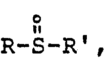
- suitable organic oxygen-containing compounds are alcohols having the formula, R-OH; ethers having the formula R-0-R'; aldehydes having the formula, ketones having the formula, esters having the formula, ; amides having the formula and sulfoxides having the formula where R and R' are alkyl.,preferably lower alkylr ; to mention but a few of the possible organic oxidants which might be used.
- the composition of the gaseous streams can be varied.
- the organozinc vapor is produced by vaporizing the organozinc compound into the gas stream, for example by bubbling a stream of inert gas through a reservoir of organozinc compound. Other vaporization methods are equally effective.
- the mole fraction of the organozinc compound in its carrier gas stream can be up to about 0.5. A mole fraction of about 0.2 is especially preferred.
- the oxidant is similarly introduced into the deposition chamber by any suitable method.
- Bubbling an inert gas through a reservoir of deionized water to produce a mixture of inert carrier gas and water vapor is an effective method for introducing water vapor.
- the mole fraction of water vapor or other oxidant in its carrier gas stream can be up to about 0.5.
- the proportion of oxidant to organozinc compound can be varied depending upon the particular properties of the zinc oxide film desired. In general, an excess of oxidant is desirable. Films deposited using excess organozinc compound have markedly higher resistivities and display poor adhesion to the substrate. A range of about 1-3 moles oxidant per mole of organozinc compound can be used.
- the flow rates of the mixture of inert gas and organozinc compound, and the mixture of the inert gas and oxidant can be varied depending upon the particular mole ratios and partial pressures of reactants which are intended to be reacted at the surface of the substrate.
- flow rates of the mixture of the inert gas and organozinc compound and inert gas and oxidant should be in the range of about 5 SCCM to 100 SCCM per square foot of deposition surface.
- the inert gas used as a carrier for the organo zinc vapor and the oxidant can be any inert gas, for example, argon or helium, or any gas which is inert under the conditions prevailing in the deposition chamber, such as nitrogen.
- Pressures within the deposition chamber in the range of about 0.1 torr to 2 torr have been found to facilitate the deposition process. Pressures can be varied by control of the reactant gas streams or by means of a regulated pumping system.
- the hydrogen-containing zinc oxide deposited according to the process of the present invention has been found to have a resistivity in the range of about 10- 4 to 10- 2 ohm-centimeter and a light transmission of greater than 90%.
- the resistivity can be reduced by adding group III elements to the zinc oxide film.
- group III elements For example, aluminum can be introduced by using trimethyl aluminum, (CH 3 )3Al. 'Similarly, boron can be introduced by utilizing diborane, B 2 H 6 .
- Gallium and indium can also be used as additives. Addition of about 1-4 mole percent of the selected additive or additives based on the organozinc vapor content has been found to be desirable. Addition of about 2 mole percent is preferred.
- diborane is introduced in a stream of inert gas, such as argon, along with the organozinc compound and oxidant.
- inert gas such as argon
- Boron-containing zinc oxide layers produced in accordance with the process of the present invention have been found to have resistivities in the range of about 5 x 10- 4 ohm-centimeter to 2.5 x 10- 3 ohm-centimeter.
- Aluminum-containing zinc oxide layers have been found to have resistivities in the range of about 1.0 x 10- 3 ohm-centimeter to 2 x 10- 3 ohm-centimeter.
- Zinc oxide films can be deposited to any desired thickness by controlling the time and rate of deposition. Typical films are 1-2 microns thick.
- the polycrystalline boron containing zinc oxide formed is found to have an x-ray diffraction pattern corresponding predominantly to (002) orientation with respect to the plane of the substrate, whereas aluminum containing zinc oxide has (100) preferred orientation.
Landscapes
- Chemical & Material Sciences (AREA)
- Inorganic Chemistry (AREA)
- General Chemical & Material Sciences (AREA)
- Chemical Kinetics & Catalysis (AREA)
- Engineering & Computer Science (AREA)
- Materials Engineering (AREA)
- Mechanical Engineering (AREA)
- Metallurgy (AREA)
- Organic Chemistry (AREA)
- Chemical Vapour Deposition (AREA)
- Photovoltaic Devices (AREA)
Abstract
Description
- The present invention relates generally to the deposition of zinc oxide films. In one of its more particular aspects, this invention relates to zinc oxide films useful in photoconductive applications deposited by an improved chemical vapor deposition process.
- In many applications where a zinc oxide film is deposited upon a heat-sensitive substrate, such as a photoconductive layer or layers, it is not desirable to deposit the zinc oxide at temperatures which may adversely affect the substrate. Although zinc oxide films have also been produced by chemical vapor deposition, such films have generally been produced only at high temperatures, for example, at temperatures of 350* to 730° C. In addition, films so produced have been characterized by relatively high resistivities.
- It is accordingly an object of the present invention to provide a process for depositing a zinc oxide film at a relatively low temperature.
- Another object of this invention is to provide such a process in which various additives can be conveniently added to the zinc oxide during deposition of the film to decrease the resistivity thereof.
- Other objects and advantages of the present invention will become apparent from the following detailed description.
- The present invention utilizes an improved chemical vapor deposition (CVD) process for depositing zinc oxide films having properties which make them useful in photoconductive applications such as in solar cells and other photovoltaic devices. The process includes introducing an organozinc compound, an oxidant and an inert carrier gas into a chamber containing a substrate heated to a temperature in the range of about 60° to 350° C. The resulting zinc oxide films may have a resistivity in the range of about 10-4 to 10-2 ohm-centimeter. Such films may contain hydrogen and may be fabricated to contain a group III element by introducing volatile group III compounds into the chamber along with the organozinc compound and oxidant.
- In general, the present invention relates to an improved chemical vapor deposition process for depositing doped zinc oxide films upon substrates such as photoconductors. Since many photoconductors are heat sensitive, it is an advantage of this invention that the deposition of zinc oxide, according to the process of the present invention, does not require high temperatures. Another advantage is that the resistivity of the resulting zinc oxide film can be varied by the use of suitable additives. In fact, the resistivity can be varied during the deposition process to produce a film or layer in which the resistivity varies from bottom to top. Another advantage is the low cost of depositing zinc oxide films using the improved CVD process of this invention.
- The process is conducted by introducing an organozinc compound, an oxidant, and any desired volatile additive into a chamber containing the desired substrate, which is heated to a temperature within the range of about 60° to 350° C, preferably 100° - 200" and more especially to a temperature of about 150° C. By heating the substrate, deposition of zinc oxide upon the walls of the chamber is avoided. In addition, deposition takes place only upon those areas of the substrate which are heated, thus making it possible to deposit a zinc oxide layer upon the entire surface of the substrate or only selected portions thereof.
- The system tor depositing zinc oxide films in accordance with one embodiment of the present invention utilises a chamber containing a heated table, means for introducing the reactants into the chamber in gaseous form and a regulated pumping system to provide a dynamic gas flow through the chamber. An organozinc compound and oxidant are carried into the chamber in individual streams of an inert carrier gas. Mixing of the organozinc vapor and oxidant occurs before contact with the heated surface of the substrate in the space between the point of introduction thereof and the heated substrate surface. Reaction between the organozinc compound and oxidant results in decomposition of the organozinc compound to produce zinc oxide, which is deposited upon the substrate as a thin film, with C02, CO and volatile hydrocarbons as possible byproducts of the reaction. The zinc oxide film contains hydrogen and may contain a group III element where a volatile compound of a group III element is also introduced into the deposition chamber.
- Suitable organozinc compounds include zinc dialkyls having the formula R2Zn, wherein R is an alkyl radical, preferably a lower alkyl radical. Dimethyl zinc, (CH3)2Zn and diethyl zinc, (C2H5)2Zn are particularly preferred.
- Suitable oxidants include water, oxygen, ozone, hydrogen peroxide, nitric oxide, nitrous oxide, nitrogen dioxide, carbon dioxide, sulfur dioxide and other oxygen-containing gases as well as organic oxygen-containing compounds. Representative of suitable organic oxygen-containing compounds are alcohols having the formula, R-OH; ethers having the formula R-0-R'; aldehydes having the formula,


- The composition of the gaseous streams can be varied. The organozinc vapor is produced by vaporizing the organozinc compound into the gas stream, for example by bubbling a stream of inert gas through a reservoir of organozinc compound. Other vaporization methods are equally effective. The mole fraction of the organozinc compound in its carrier gas stream can be up to about 0.5. A mole fraction of about 0.2 is especially preferred.
- The oxidant is similarly introduced into the deposition chamber by any suitable method. Bubbling an inert gas through a reservoir of deionized water to produce a mixture of inert carrier gas and water vapor, for example, is an effective method for introducing water vapor. The mole fraction of water vapor or other oxidant in its carrier gas stream can be up to about 0.5.
- The proportion of oxidant to organozinc compound can be varied depending upon the particular properties of the zinc oxide film desired. In general, an excess of oxidant is desirable. Films deposited using excess organozinc compound have markedly higher resistivities and display poor adhesion to the substrate. A range of about 1-3 moles oxidant per mole of organozinc compound can be used.
- The flow rates of the mixture of inert gas and organozinc compound, and the mixture of the inert gas and oxidant can be varied depending upon the particular mole ratios and partial pressures of reactants which are intended to be reacted at the surface of the substrate. For example, where bubblers are used to introduce the reactants, flow rates of the mixture of the inert gas and organozinc compound and inert gas and oxidant should be in the range of about 5 SCCM to 100 SCCM per square foot of deposition surface.
- The inert gas used as a carrier for the organo zinc vapor and the oxidant can be any inert gas, for example, argon or helium, or any gas which is inert under the conditions prevailing in the deposition chamber, such as nitrogen.
- Pressures within the deposition chamber in the range of about 0.1 torr to 2 torr have been found to facilitate the deposition process. Pressures can be varied by control of the reactant gas streams or by means of a regulated pumping system.
- The hydrogen-containing zinc oxide deposited according to the process of the present invention has been found to have a resistivity in the range of about 10-4 to 10-2 ohm-centimeter and a light transmission of greater than 90%. The resistivity can be reduced by adding group III elements to the zinc oxide film. For example, aluminum can be introduced by using trimethyl aluminum, (CH3)3Al. 'Similarly, boron can be introduced by utilizing diborane, B2H6. Gallium and indium can also be used as additives. Addition of about 1-4 mole percent of the selected additive or additives based on the organozinc vapor content has been found to be desirable. Addition of about 2 mole percent is preferred. Where boron is to be incorporated into the zinc oxide film, diborane is introduced in a stream of inert gas, such as argon, along with the organozinc compound and oxidant. Boron-containing zinc oxide layers produced in accordance with the process of the present invention have been found to have resistivities in the range of about 5 x 10⁻⁴ ohm-centimeter to 2.5 x 10⁻³ ohm-centimeter. Aluminum-containing zinc oxide layers have been found to have resistivities in the range of about 1.0 x 10⁻³ ohm-centimeter to 2 x 10⁻³ ohm-centimeter.
- Deposition rates of about 200 Angstroms per minute at 125° C. and 600 Angstroms per minute at 150° C. are readily attainable. Rates are also controlled in part by gas flow rates and partial pressures of reactants. Zinc oxide films can be deposited to any desired thickness by controlling the time and rate of deposition. Typical films are 1-2 microns thick. The polycrystalline boron containing zinc oxide formed is found to have an x-ray diffraction pattern corresponding predominantly to (002) orientation with respect to the plane of the substrate, whereas aluminum containing zinc oxide has (100) preferred orientation.
- By means of the process of the present invention, it is thus possible to deposit large areas of zinc oxide and to control the resistivity thereof. In this manner, for example, conductive zinc oxide layers for use in solar cells can be readily deposited. Depending upon the particular additive utilized in the process, it is also possible to produce other zinc oxide layers for use in photoconductive devices and having varying physical and electrical properties.
- While certain specific embodiments of the invention have been disclosed as typical, the invention is, of course, not limited to these particular forms, but rather is applicable to all such variations as fall within the scope of the intended claims. For example, other group III additives than aluminum and boron can be used to provide zinc oxide layers having varying properties. In addition, various other reaction conditions than those specifically mentioned above can be used in the process of the present invention.
Claims (14)


Applications Claiming Priority (2)
| Application Number | Priority Date | Filing Date | Title |
|---|---|---|---|
| US74108185A | 1985-06-04 | 1985-06-04 | |
| US741081 | 1985-06-04 |
Publications (3)
| Publication Number | Publication Date |
|---|---|
| EP0204563A2 true EP0204563A2 (en) | 1986-12-10 |
| EP0204563A3 EP0204563A3 (en) | 1988-09-07 |
| EP0204563B1 EP0204563B1 (en) | 1993-01-20 |
Family
ID=24979305
Family Applications (1)
| Application Number | Title | Priority Date | Filing Date |
|---|---|---|---|
| EP19860304269 Expired - Lifetime EP0204563B1 (en) | 1985-06-04 | 1986-06-04 | Process for depositing zinc oxide |
Country Status (4)
| Country | Link |
|---|---|
| US (1) | US4751149A (en) |
| EP (1) | EP0204563B1 (en) |
| JP (1) | JPH0682625B2 (en) |
| DE (1) | DE3687540T2 (en) |
Cited By (7)
| Publication number | Priority date | Publication date | Assignee | Title |
|---|---|---|---|---|
| DE3916983A1 (en) * | 1988-05-25 | 1989-11-30 | Canon Kk | METHOD FOR FORMING FUNCTIONAL ZINCOXIDE FILMS USING ALKYLZINK COMPOUND AND OXYGEN-CONTAINING GAS |
| EP0335769A3 (en) * | 1988-03-30 | 1990-08-29 | Saint-Gobain Vitrage International | Electroconducting glass and method of making the same |
| GB2261444A (en) * | 1991-11-12 | 1993-05-19 | Fujitsu Ltd | Chemical vapor phase growth of silicides in the presence of water |
| US6808743B2 (en) | 2000-06-06 | 2004-10-26 | Unisearch Limited | Growth of ZnO film using single source CVD |
| EP1788119A1 (en) * | 2005-11-21 | 2007-05-23 | Air Products and Chemicals, Inc. | Method for depositing zinc oxide at low temperatures and products formed thereby |
| EP1840966A1 (en) | 2006-03-30 | 2007-10-03 | Universite De Neuchatel | Transparent, conducting and textured layer and method of fabrication |
| EP2101347A1 (en) * | 2008-03-04 | 2009-09-16 | KISCO Corporation | Annealing method of zinc oxide thin film |
Families Citing this family (101)
| Publication number | Priority date | Publication date | Assignee | Title |
|---|---|---|---|---|
| US5200388A (en) * | 1988-05-13 | 1993-04-06 | Oki Electric Industry Co., Ltd. | Metalorganic chemical vapor deposition of superconducting films |
| US5252499A (en) * | 1988-08-15 | 1993-10-12 | Rothschild G F Neumark | Wide band-gap semiconductors having low bipolar resistivity and method of formation |
| US4873118A (en) * | 1988-11-18 | 1989-10-10 | Atlantic Richfield Company | Oxygen glow treating of ZnO electrode for thin film silicon solar cell |
| US4990286A (en) * | 1989-03-17 | 1991-02-05 | President And Fellows Of Harvard College | Zinc oxyfluoride transparent conductor |
| US5078803A (en) * | 1989-09-22 | 1992-01-07 | Siemens Solar Industries L.P. | Solar cells incorporating transparent electrodes comprising hazy zinc oxide |
| US4980198A (en) * | 1989-11-30 | 1990-12-25 | Syracuse University | Laser CVD and plasma CVD of CrO2 films and cobalt doped CrO2 films using organometallic precursors |
| US5124180A (en) * | 1991-03-11 | 1992-06-23 | Btu Engineering Corporation | Method for the formation of fluorine doped metal oxide films |
| JP2545306B2 (en) * | 1991-03-11 | 1996-10-16 | 誠 小長井 | Method for producing ZnO transparent conductive film |
| EP0578046B1 (en) * | 1992-07-10 | 1996-11-06 | Asahi Glass Company Ltd. | Transparent conductive film, and target and material for vapor deposition to be used for its production |
| US5383088A (en) * | 1993-08-09 | 1995-01-17 | International Business Machines Corporation | Storage capacitor with a conducting oxide electrode for metal-oxide dielectrics |
| GB9616983D0 (en) | 1996-08-13 | 1996-09-25 | Pilkington Plc | Method for depositing tin oxide and titanium oxide coatings on flat glass and the resulting coated glass |
| US6238738B1 (en) | 1996-08-13 | 2001-05-29 | Libbey-Owens-Ford Co. | Method for depositing titanium oxide coatings on flat glass |
| US6027766A (en) * | 1997-03-14 | 2000-02-22 | Ppg Industries Ohio, Inc. | Photocatalytically-activated self-cleaning article and method of making same |
| US7096692B2 (en) * | 1997-03-14 | 2006-08-29 | Ppg Industries Ohio, Inc. | Visible-light-responsive photoactive coating, coated article, and method of making same |
| AUPO663597A0 (en) * | 1997-05-06 | 1997-05-29 | Unisearch Limited | Fabrication of zinc oxide films in non-planar substrates and the use thereof |
| US6071561A (en) * | 1997-08-13 | 2000-06-06 | President And Fellows Of Harvard College | Chemical vapor deposition of fluorine-doped zinc oxide |
| US5948176A (en) * | 1997-09-29 | 1999-09-07 | Midwest Research Institute | Cadmium-free junction fabrication process for CuInSe2 thin film solar cells |
| GB9913315D0 (en) | 1999-06-08 | 1999-08-11 | Pilkington Plc | Improved process for coating glass |
| US6416814B1 (en) * | 2000-12-07 | 2002-07-09 | First Solar, Llc | Volatile organometallic complexes of lowered reactivity suitable for use in chemical vapor deposition of metal oxide films |
| EP1289025A1 (en) * | 2001-08-30 | 2003-03-05 | Universite De Neuchatel | Method to deposit an oxyde layer on a substrate and photovoltaic cell using such substrate |
| JP4108633B2 (en) * | 2003-06-20 | 2008-06-25 | シャープ株式会社 | THIN FILM TRANSISTOR, MANUFACTURING METHOD THEREOF, AND ELECTRONIC DEVICE |
| US7179677B2 (en) * | 2003-09-03 | 2007-02-20 | Midwest Research Institute | ZnO/Cu(InGa)Se2 solar cells prepared by vapor phase Zn doping |
| JP4939058B2 (en) * | 2004-02-16 | 2012-05-23 | 株式会社カネカ | Method for producing transparent conductive film and method for producing tandem-type thin film photoelectric conversion device |
| JP4699092B2 (en) * | 2005-06-01 | 2011-06-08 | 日本パイオニクス株式会社 | Method for forming zinc oxide film |
| GB0518383D0 (en) * | 2005-09-09 | 2005-10-19 | Pilkington Plc | Deposition process |
| DE602006016008D1 (en) * | 2005-12-21 | 2010-09-16 | Saint Gobain | PROCESS FOR MANUFACTURING A PHOTOVOLTAIC THIN FILM COMPONENT |
| WO2007130447A2 (en) * | 2006-05-05 | 2007-11-15 | Pilkington Group Limited | Method for depositing zinc oxide coatings on flat glass |
| BRPI0711292A2 (en) * | 2006-05-05 | 2011-08-23 | Arkema Inc | vapor phase chemical deposition process for the deposition of a zinc oxide coating on a continuous heated glass substrate during a float glass manufacturing process |
| US8017860B2 (en) * | 2006-05-15 | 2011-09-13 | Stion Corporation | Method and structure for thin film photovoltaic materials using bulk semiconductor materials |
| US9105776B2 (en) * | 2006-05-15 | 2015-08-11 | Stion Corporation | Method and structure for thin film photovoltaic materials using semiconductor materials |
| US8158262B2 (en) * | 2006-06-05 | 2012-04-17 | Pilkington Group Limited | Glass article having a zinc oxide coating and method for making same |
| MX2009002181A (en) * | 2006-08-29 | 2009-04-22 | Pilkington Group Ltd | Method of forming a zinc oxide coated article. |
| US8163342B2 (en) * | 2006-08-29 | 2012-04-24 | Pilkington Group Limited | Method of making low resisitivity doped zinc oxide coatings and the articles formed thereby |
| BRPI0716385A2 (en) * | 2006-08-29 | 2013-01-01 | Pilkington Group Ltd E Arkema Inc | method for preparing a low resistivity doped zinc oxide coated glass article, atmospheric pressure chemical vapor deposition method for preparing a doped zinc oxide coated glass article, atmospheric pressure chemical vapor deposition method for prepare a doped zinc oxide coated article, and glass article |
| US7740901B2 (en) * | 2006-09-08 | 2010-06-22 | Pilkington Group Limited | Low temperature method of making a zinc oxide coated article and the coated article made thereby |
| WO2008059857A1 (en) * | 2006-11-17 | 2008-05-22 | Kaneka Corporation | Thin-film photoelectric conversion device |
| US8066840B2 (en) * | 2007-01-22 | 2011-11-29 | Solopower, Inc. | Finger pattern formation for thin film solar cells |
| DE112008001372T5 (en) * | 2007-05-22 | 2010-04-15 | National University Corporation Nagaoka University of Technology, Nagaoka-shi | Method and apparatus for forming a metal oxide thin film |
| US20080300918A1 (en) * | 2007-05-29 | 2008-12-04 | Commercenet Consortium, Inc. | System and method for facilitating hospital scheduling and support |
| US8071179B2 (en) * | 2007-06-29 | 2011-12-06 | Stion Corporation | Methods for infusing one or more materials into nano-voids if nanoporous or nanostructured materials |
| US7919400B2 (en) * | 2007-07-10 | 2011-04-05 | Stion Corporation | Methods for doping nanostructured materials and nanostructured thin films |
| US8759671B2 (en) | 2007-09-28 | 2014-06-24 | Stion Corporation | Thin film metal oxide bearing semiconductor material for single junction solar cell devices |
| US8058092B2 (en) | 2007-09-28 | 2011-11-15 | Stion Corporation | Method and material for processing iron disilicide for photovoltaic application |
| US8287942B1 (en) | 2007-09-28 | 2012-10-16 | Stion Corporation | Method for manufacture of semiconductor bearing thin film material |
| US8614396B2 (en) * | 2007-09-28 | 2013-12-24 | Stion Corporation | Method and material for purifying iron disilicide for photovoltaic application |
| US8187434B1 (en) | 2007-11-14 | 2012-05-29 | Stion Corporation | Method and system for large scale manufacture of thin film photovoltaic devices using single-chamber configuration |
| US8440903B1 (en) | 2008-02-21 | 2013-05-14 | Stion Corporation | Method and structure for forming module using a powder coating and thermal treatment process |
| US8772078B1 (en) | 2008-03-03 | 2014-07-08 | Stion Corporation | Method and system for laser separation for exclusion region of multi-junction photovoltaic materials |
| US8075723B1 (en) | 2008-03-03 | 2011-12-13 | Stion Corporation | Laser separation method for manufacture of unit cells for thin film photovoltaic materials |
| US7939454B1 (en) | 2008-05-31 | 2011-05-10 | Stion Corporation | Module and lamination process for multijunction cells |
| US8642138B2 (en) | 2008-06-11 | 2014-02-04 | Stion Corporation | Processing method for cleaning sulfur entities of contact regions |
| US9087943B2 (en) | 2008-06-25 | 2015-07-21 | Stion Corporation | High efficiency photovoltaic cell and manufacturing method free of metal disulfide barrier material |
| US8003432B2 (en) | 2008-06-25 | 2011-08-23 | Stion Corporation | Consumable adhesive layer for thin film photovoltaic material |
| US8822263B2 (en) * | 2008-06-30 | 2014-09-02 | National University Corporation Tokyo University Of Agriculture And Technology | Epitaxial growth method of a zinc oxide based semiconductor layer, epitaxial crystal structure, epitaxial crystal growth apparatus, and semiconductor device |
| US8207008B1 (en) | 2008-08-01 | 2012-06-26 | Stion Corporation | Affixing method and solar decal device using a thin film photovoltaic |
| US7855089B2 (en) | 2008-09-10 | 2010-12-21 | Stion Corporation | Application specific solar cell and method for manufacture using thin film photovoltaic materials |
| US8026122B1 (en) | 2008-09-29 | 2011-09-27 | Stion Corporation | Metal species surface treatment of thin film photovoltaic cell and manufacturing method |
| US8394662B1 (en) | 2008-09-29 | 2013-03-12 | Stion Corporation | Chloride species surface treatment of thin film photovoltaic cell and manufacturing method |
| US8008112B1 (en) | 2008-09-29 | 2011-08-30 | Stion Corporation | Bulk chloride species treatment of thin film photovoltaic cell and manufacturing method |
| US8008110B1 (en) | 2008-09-29 | 2011-08-30 | Stion Corporation | Bulk sodium species treatment of thin film photovoltaic cell and manufacturing method |
| US8476104B1 (en) | 2008-09-29 | 2013-07-02 | Stion Corporation | Sodium species surface treatment of thin film photovoltaic cell and manufacturing method |
| US8236597B1 (en) | 2008-09-29 | 2012-08-07 | Stion Corporation | Bulk metal species treatment of thin film photovoltaic cell and manufacturing method |
| US8501521B1 (en) | 2008-09-29 | 2013-08-06 | Stion Corporation | Copper species surface treatment of thin film photovoltaic cell and manufacturing method |
| US8383450B2 (en) | 2008-09-30 | 2013-02-26 | Stion Corporation | Large scale chemical bath system and method for cadmium sulfide processing of thin film photovoltaic materials |
| US7910399B1 (en) * | 2008-09-30 | 2011-03-22 | Stion Corporation | Thermal management and method for large scale processing of CIS and/or CIGS based thin films overlying glass substrates |
| US8425739B1 (en) | 2008-09-30 | 2013-04-23 | Stion Corporation | In chamber sodium doping process and system for large scale cigs based thin film photovoltaic materials |
| US7947524B2 (en) | 2008-09-30 | 2011-05-24 | Stion Corporation | Humidity control and method for thin film photovoltaic materials |
| US7863074B2 (en) | 2008-09-30 | 2011-01-04 | Stion Corporation | Patterning electrode materials free from berm structures for thin film photovoltaic cells |
| US8741689B2 (en) | 2008-10-01 | 2014-06-03 | Stion Corporation | Thermal pre-treatment process for soda lime glass substrate for thin film photovoltaic materials |
| US20110018103A1 (en) | 2008-10-02 | 2011-01-27 | Stion Corporation | System and method for transferring substrates in large scale processing of cigs and/or cis devices |
| US8003430B1 (en) | 2008-10-06 | 2011-08-23 | Stion Corporation | Sulfide species treatment of thin film photovoltaic cell and manufacturing method |
| US8435826B1 (en) | 2008-10-06 | 2013-05-07 | Stion Corporation | Bulk sulfide species treatment of thin film photovoltaic cell and manufacturing method |
| USD625695S1 (en) | 2008-10-14 | 2010-10-19 | Stion Corporation | Patterned thin film photovoltaic module |
| US8168463B2 (en) | 2008-10-17 | 2012-05-01 | Stion Corporation | Zinc oxide film method and structure for CIGS cell |
| US8344243B2 (en) | 2008-11-20 | 2013-01-01 | Stion Corporation | Method and structure for thin film photovoltaic cell using similar material junction |
| USD662040S1 (en) | 2009-06-12 | 2012-06-19 | Stion Corporation | Pin striped thin film solar module for garden lamp |
| USD628332S1 (en) | 2009-06-12 | 2010-11-30 | Stion Corporation | Pin striped thin film solar module for street lamp |
| USD632415S1 (en) | 2009-06-13 | 2011-02-08 | Stion Corporation | Pin striped thin film solar module for cluster lamp |
| US9528182B2 (en) | 2009-06-22 | 2016-12-27 | Arkema Inc. | Chemical vapor deposition using N,O polydentate ligand complexes of metals |
| USD662041S1 (en) | 2009-06-23 | 2012-06-19 | Stion Corporation | Pin striped thin film solar module for laptop personal computer |
| USD652262S1 (en) | 2009-06-23 | 2012-01-17 | Stion Corporation | Pin striped thin film solar module for cooler |
| US8507786B1 (en) | 2009-06-27 | 2013-08-13 | Stion Corporation | Manufacturing method for patterning CIGS/CIS solar cells |
| USD627696S1 (en) | 2009-07-01 | 2010-11-23 | Stion Corporation | Pin striped thin film solar module for recreational vehicle |
| US8398772B1 (en) | 2009-08-18 | 2013-03-19 | Stion Corporation | Method and structure for processing thin film PV cells with improved temperature uniformity |
| WO2011047114A1 (en) * | 2009-10-15 | 2011-04-21 | Arkema Inc. | Deposition of doped zno films on polymer substrates by uv-assisted chemical vapor deposition |
| US8809096B1 (en) | 2009-10-22 | 2014-08-19 | Stion Corporation | Bell jar extraction tool method and apparatus for thin film photovoltaic materials |
| US8859880B2 (en) | 2010-01-22 | 2014-10-14 | Stion Corporation | Method and structure for tiling industrial thin-film solar devices |
| US8263494B2 (en) | 2010-01-25 | 2012-09-11 | Stion Corporation | Method for improved patterning accuracy for thin film photovoltaic panels |
| US9096930B2 (en) | 2010-03-29 | 2015-08-04 | Stion Corporation | Apparatus for manufacturing thin film photovoltaic devices |
| JP5559620B2 (en) * | 2010-07-07 | 2014-07-23 | 株式会社カネカ | Substrate with transparent conductive film |
| US8461061B2 (en) | 2010-07-23 | 2013-06-11 | Stion Corporation | Quartz boat method and apparatus for thin film thermal treatment |
| US8906732B2 (en) * | 2010-10-01 | 2014-12-09 | Stion Corporation | Method and device for cadmium-free solar cells |
| US8628997B2 (en) * | 2010-10-01 | 2014-01-14 | Stion Corporation | Method and device for cadmium-free solar cells |
| US8998606B2 (en) | 2011-01-14 | 2015-04-07 | Stion Corporation | Apparatus and method utilizing forced convection for uniform thermal treatment of thin film devices |
| US8728200B1 (en) | 2011-01-14 | 2014-05-20 | Stion Corporation | Method and system for recycling processing gas for selenization of thin film photovoltaic materials |
| EP2688850B1 (en) * | 2011-03-23 | 2018-02-21 | Pilkington Group Limited | Method of depositing zinc oxide coatings by chemical vapor deposition |
| US8436445B2 (en) | 2011-08-15 | 2013-05-07 | Stion Corporation | Method of manufacture of sodium doped CIGS/CIGSS absorber layers for high efficiency photovoltaic devices |
| KR20130054812A (en) * | 2011-11-17 | 2013-05-27 | 삼성코닝정밀소재 주식회사 | Zinc oxide precursor and method of depositing zinc oxide-based thin film using the same |
| KR20140046617A (en) * | 2012-10-09 | 2014-04-21 | 삼성코닝정밀소재 주식회사 | Zinc oxide precursor and method of depositing zinc oxide-based thin film using the same |
| KR20140068588A (en) * | 2012-11-28 | 2014-06-09 | 코닝정밀소재 주식회사 | Method of fabricating zinc oxide thin film |
| DE102016118345A1 (en) | 2016-08-01 | 2018-02-01 | Aixtron Se | Conditioning process for a CVD reactor |
Family Cites Families (6)
| Publication number | Priority date | Publication date | Assignee | Title |
|---|---|---|---|---|
| US1420888A (en) * | 1922-06-27 | Aeteehes d | ||
| US3081200A (en) * | 1959-04-10 | 1963-03-12 | Armour Res Found | Method of applying an oxide coating onto a non-porous refractory substrate |
| US3655429A (en) * | 1969-04-16 | 1972-04-11 | Westinghouse Electric Corp | Method of forming thin insulating films particularly for piezoelectric transducers |
| US4051276A (en) * | 1974-12-24 | 1977-09-27 | The United States Government As Represented By The Librarian Of Congress | Method of deacidifying paper |
| US3969549A (en) * | 1974-12-24 | 1976-07-13 | The United States Of America As Represented By The Librarian Of Congress | Method of deacidifying paper |
| JPS51144183A (en) * | 1975-06-06 | 1976-12-10 | Hitachi Ltd | Semiconductor element containing surface protection film |
-
1986
- 1986-05-26 JP JP11942286A patent/JPH0682625B2/en not_active Expired - Lifetime
- 1986-06-04 EP EP19860304269 patent/EP0204563B1/en not_active Expired - Lifetime
- 1986-06-04 DE DE8686304269T patent/DE3687540T2/en not_active Expired - Lifetime
-
1987
- 1987-03-12 US US07/024,871 patent/US4751149A/en not_active Expired - Lifetime
Cited By (12)
| Publication number | Priority date | Publication date | Assignee | Title |
|---|---|---|---|---|
| EP0335769A3 (en) * | 1988-03-30 | 1990-08-29 | Saint-Gobain Vitrage International | Electroconducting glass and method of making the same |
| DE3916983A1 (en) * | 1988-05-25 | 1989-11-30 | Canon Kk | METHOD FOR FORMING FUNCTIONAL ZINCOXIDE FILMS USING ALKYLZINK COMPOUND AND OXYGEN-CONTAINING GAS |
| GB2261444A (en) * | 1991-11-12 | 1993-05-19 | Fujitsu Ltd | Chemical vapor phase growth of silicides in the presence of water |
| US5298278A (en) * | 1991-11-12 | 1994-03-29 | Fujitsu Limited | Chemical vapor phase growth method and chemical vapor phase growth apparatus |
| GB2261444B (en) * | 1991-11-12 | 1994-11-23 | Fujitsu Ltd | Chemical vapor phase growth method and chemical vapor phase growth apparatus |
| US6808743B2 (en) | 2000-06-06 | 2004-10-26 | Unisearch Limited | Growth of ZnO film using single source CVD |
| EP1788119A1 (en) * | 2005-11-21 | 2007-05-23 | Air Products and Chemicals, Inc. | Method for depositing zinc oxide at low temperatures and products formed thereby |
| US8197914B2 (en) | 2005-11-21 | 2012-06-12 | Air Products And Chemicals, Inc. | Method for depositing zinc oxide at low temperatures and products formed thereby |
| TWI461560B (en) * | 2005-11-21 | 2014-11-21 | 氣體產品及化學品股份公司 | Method for depositing zinc oxide at low temperature and products formed thereby |
| EP1840966A1 (en) | 2006-03-30 | 2007-10-03 | Universite De Neuchatel | Transparent, conducting and textured layer and method of fabrication |
| EP2101347A1 (en) * | 2008-03-04 | 2009-09-16 | KISCO Corporation | Annealing method of zinc oxide thin film |
| US8034656B2 (en) | 2008-03-04 | 2011-10-11 | Kisco | Annealing method of zinc oxide thin film |
Also Published As
| Publication number | Publication date |
|---|---|
| DE3687540T2 (en) | 1993-08-05 |
| JPH0682625B2 (en) | 1994-10-19 |
| JPS627123A (en) | 1987-01-14 |
| EP0204563A3 (en) | 1988-09-07 |
| DE3687540D1 (en) | 1993-03-04 |
| US4751149A (en) | 1988-06-14 |
| EP0204563B1 (en) | 1993-01-20 |
Similar Documents
| Publication | Publication Date | Title |
|---|---|---|
| US4751149A (en) | Chemical vapor deposition of zinc oxide films and products | |
| US4791005A (en) | Method for the manufacture of silicon oxide layers doped with boron and phosphorus | |
| DE68909774T2 (en) | Deposition of silicon dioxide films based on liquid alkylsilanes. | |
| US5607722A (en) | Process for titanium nitride deposition using five-and six-coordinate titanium complexes | |
| US5360646A (en) | Chemical vapor deposition method of silicon dioxide film | |
| WO1990003452A1 (en) | Chemical vapor deposition of silicon carbide | |
| KR940004714A (en) | Supersaturated rare earth element doped semiconductor layer by chemical vapor deposition | |
| WO1991008322A1 (en) | Process for chemical vapor deposition of transition metal nitrides | |
| KR20000049201A (en) | Chemical vapor deposition of aluminum oxide | |
| EP0232619A2 (en) | Method of manufacturing a thin-film transistor | |
| EP0212691A1 (en) | Low temperature chemical vapor deposition of silicon dioxide films | |
| KR910000509B1 (en) | Method for Photochemical Deposition of Oxide Layers at Enhanced Deposition Rates | |
| US5082696A (en) | Method of forming semiconducting amorphous silicon films from the thermal decomposition of dihalosilanes | |
| Chu et al. | Deposition and properties of silicon on graphite substrates | |
| He et al. | Ion-beam-assisted deposition of Si-carbide films | |
| WO2007130448A2 (en) | Method of depositing zinc oxide coatings on a substrate | |
| Reich et al. | Plasma-enhanced chemical vapour deposition of thin GeO2, SnOx, GeO2 SnOx, and In2O3 films | |
| US3761308A (en) | Preparation of photoconductive films | |
| US5882805A (en) | Chemical vapor deposition of II/VI semiconductor material using triisopropylindium as a dopant | |
| TWI711622B (en) | Bis(alkyltetramethylcyclopentadiene) zinc, raw material for chemical vapor deposition, and manufacturing method of zinc-containing film | |
| CA1335950C (en) | Method of forming semiconducting amorphous silicon films from the thermal decomposition of dihalosilanes | |
| Wong et al. | 11 Patent Number: 4,751,149 (45) Date of Patent: Jun. 14, 1988 | |
| Runyan et al. | Behavior of Large‐Scale Surface Perturbations during Silicon Epitaxial Growth | |
| US20060198958A1 (en) | Methods for producing silicon nitride films by vapor-phase growth | |
| JPS60169563A (en) | Manufacture and device for telluride metal |
Legal Events
| Date | Code | Title | Description |
|---|---|---|---|
| PUAI | Public reference made under article 153(3) epc to a published international application that has entered the european phase |
Free format text: ORIGINAL CODE: 0009012 |
|
| AK | Designated contracting states |
Kind code of ref document: A2 Designated state(s): DE FR GB IT NL |
|
| PUAL | Search report despatched |
Free format text: ORIGINAL CODE: 0009013 |
|
| AK | Designated contracting states |
Kind code of ref document: A3 Designated state(s): DE FR GB IT NL |
|
| 17P | Request for examination filed |
Effective date: 19890227 |
|
| 17Q | First examination report despatched |
Effective date: 19900919 |
|
| RAP1 | Party data changed (applicant data changed or rights of an application transferred) |
Owner name: SIEMENS SOLAR INDUSTRIES L.P. |
|
| GRAA | (expected) grant |
Free format text: ORIGINAL CODE: 0009210 |
|
| AK | Designated contracting states |
Kind code of ref document: B1 Designated state(s): DE FR GB IT NL |
|
| REF | Corresponds to: |
Ref document number: 3687540 Country of ref document: DE Date of ref document: 19930304 |
|
| ET | Fr: translation filed | ||
| ITF | It: translation for a ep patent filed | ||
| PLBE | No opposition filed within time limit |
Free format text: ORIGINAL CODE: 0009261 |
|
| STAA | Information on the status of an ep patent application or granted ep patent |
Free format text: STATUS: NO OPPOSITION FILED WITHIN TIME LIMIT |
|
| 26N | No opposition filed | ||
| REG | Reference to a national code |
Ref country code: GB Ref legal event code: IF02 |
|
| NLT1 | Nl: modifications of names registered in virtue of documents presented to the patent office pursuant to art. 16 a, paragraph 1 |
Owner name: SHELL SOLAR INDUSTRIES LP |
|
| PGFP | Annual fee paid to national office [announced via postgrant information from national office to epo] |
Ref country code: FR Payment date: 20050427 Year of fee payment: 20 |
|
| PGFP | Annual fee paid to national office [announced via postgrant information from national office to epo] |
Ref country code: GB Payment date: 20050524 Year of fee payment: 20 |
|
| PGFP | Annual fee paid to national office [announced via postgrant information from national office to epo] |
Ref country code: NL Payment date: 20050623 Year of fee payment: 20 |
|
| PGFP | Annual fee paid to national office [announced via postgrant information from national office to epo] |
Ref country code: IT Payment date: 20050628 Year of fee payment: 20 |
|
| REG | Reference to a national code |
Ref country code: GB Ref legal event code: PE20 |
|
| PGFP | Annual fee paid to national office [announced via postgrant information from national office to epo] |
Ref country code: DE Payment date: 20050708 Year of fee payment: 20 |
|
| REG | Reference to a national code |
Ref country code: FR Ref legal event code: CD |
|
| PG25 | Lapsed in a contracting state [announced via postgrant information from national office to epo] |
Ref country code: GB Free format text: LAPSE BECAUSE OF EXPIRATION OF PROTECTION Effective date: 20060603 |
|
| PG25 | Lapsed in a contracting state [announced via postgrant information from national office to epo] |
Ref country code: NL Free format text: LAPSE BECAUSE OF EXPIRATION OF PROTECTION Effective date: 20060604 |
|
| NLV7 | Nl: ceased due to reaching the maximum lifetime of a patent |
Effective date: 20060604 |