EP0205899A1 - Photodiode à avalanche planaire à héterojonction - Google Patents
Photodiode à avalanche planaire à héterojonction Download PDFInfo
- Publication number
- EP0205899A1 EP0205899A1 EP86106627A EP86106627A EP0205899A1 EP 0205899 A1 EP0205899 A1 EP 0205899A1 EP 86106627 A EP86106627 A EP 86106627A EP 86106627 A EP86106627 A EP 86106627A EP 0205899 A1 EP0205899 A1 EP 0205899A1
- Authority
- EP
- European Patent Office
- Prior art keywords
- semiconductor layer
- junction
- conductivity type
- layer
- apd
- Prior art date
- Legal status (The legal status is an assumption and is not a legal conclusion. Google has not performed a legal analysis and makes no representation as to the accuracy of the status listed.)
- Granted
Links
Images


Classifications
-
- H—ELECTRICITY
- H10—SEMICONDUCTOR DEVICES; ELECTRIC SOLID-STATE DEVICES NOT OTHERWISE PROVIDED FOR
- H10F—INORGANIC SEMICONDUCTOR DEVICES SENSITIVE TO INFRARED RADIATION, LIGHT, ELECTROMAGNETIC RADIATION OF SHORTER WAVELENGTH OR CORPUSCULAR RADIATION
- H10F30/00—Individual radiation-sensitive semiconductor devices in which radiation controls the flow of current through the devices, e.g. photodetectors
- H10F30/20—Individual radiation-sensitive semiconductor devices in which radiation controls the flow of current through the devices, e.g. photodetectors the devices having potential barriers, e.g. phototransistors
- H10F30/21—Individual radiation-sensitive semiconductor devices in which radiation controls the flow of current through the devices, e.g. photodetectors the devices having potential barriers, e.g. phototransistors the devices being sensitive to infrared, visible or ultraviolet radiation
- H10F30/22—Individual radiation-sensitive semiconductor devices in which radiation controls the flow of current through the devices, e.g. photodetectors the devices having potential barriers, e.g. phototransistors the devices being sensitive to infrared, visible or ultraviolet radiation the devices having only one potential barrier, e.g. photodiodes
- H10F30/225—Individual radiation-sensitive semiconductor devices in which radiation controls the flow of current through the devices, e.g. photodetectors the devices having potential barriers, e.g. phototransistors the devices being sensitive to infrared, visible or ultraviolet radiation the devices having only one potential barrier, e.g. photodiodes the potential barrier working in avalanche mode, e.g. avalanche photodiodes
- H10F30/2255—Individual radiation-sensitive semiconductor devices in which radiation controls the flow of current through the devices, e.g. photodetectors the devices having potential barriers, e.g. phototransistors the devices being sensitive to infrared, visible or ultraviolet radiation the devices having only one potential barrier, e.g. photodiodes the potential barrier working in avalanche mode, e.g. avalanche photodiodes in which the active layers form heterostructures, e.g. SAM structures
Definitions
- the present invention relates to a planar heterojunction avalanche photodiode having a guard ring.
- an avalanche photodiode - using an In o . 53 Ga o . 47 As semiconductor is under way for optical communications in the 1 to 1.6 micron wavelength region, where the transmission loss of optical fibers is relatively small.
- Such a heterojunction APD uses a heterojunction of Ino. 53 Gao. 47 As and InP, which permit lattice matching to each other.
- the InGaAs layer whose bandgap is smaller, is used for light absorption, and either the electron or the positive hole carriers, generated therein by optical excitation, are transported to the p-n junction in the InP for avalanche multiplication.
- a planar structure wherein a p + region is selectively diffused in n-InP to form a stepwise p-n junction.
- a reverse bias is applied to the p-n junction, the electric field will most readily concentrate in the circumferential part of the diffused region, resulting in an earlier breakdown than in the p-n junction of the flat part of the diffused region, which is closer to the light receiving area.
- This phenomenon is known as edge breakdown; in order to prevent it there is proposed an arrangement in which the circumference of the diffused region is surrounded by a guard-ring of a linearly graded p-n junction, whose breakdown voltage is relatively high.
- T. Shirai et al. attempted to prevent edge breakdown by so forming a guard-ring that its linearly graded p-n junction front reaches the same depth as a stepwise-p-n junction (T. Shirai et al., "InGaAs Avalanche Photodiodes for 1 u.m Wavelength Region", ELECTRONIC LETTERS,7th July 1983, Vol. 19, No. 14, pp.534 -535).
- the depletion layer in a stepwise p-n junction upon application of a reverse bias, grows unidirectionally into an n-conductivity region, that in a linearly graded p-n junction grows into both p-and n-conductive regions.
- a contour having a positive curvature emerges in the depletion layer resulting from the two p-n junctions, and an electric field concentrates on the positive curvature region to invite edge breakdown.
- T. Torikai et al. tried to prevent edge breakdown by forming the linearly graded p-n junction front of a guard ring in an even deeper position than the stepwise p-n junction (T. Torikai et al., "Low Noise and High Speed InP/InGaAsP/InGaAs Avalanche Photodiodes with Planar Structure Grown by Vapor Phase Epitaxy", 10th European Conference on Optical Communication, Stuttgart, Sept, 3-6, 1984, Conference Proceedings, pp. 220-221).
- the guard ring of the linearly graded p-n junction in this structure is positioned close to the InGaAsP layer whose bandgap is smaller, it is susceptible to edge breakdown from the depletion layer's edge of the guard-ring's p-n junction, so that the front position of the linearly graded p-n junction requires critical control.
- the stepwise p f- n junction front is arranged in a high-concentration n-InP layer or at the interface between low-concentration n-InP and high-concentration n-lnP layers, so that noise reduction is restricted.
- An object of the present invention is to provide a heterojunction APD with guard-ring, which is free from the disadvantages mentioned above and yet effectively protected from edge breakdown.
- Another object of the invention is to provide a heterojunction APD permitting further noise reduction.
- a planar heterojunction avalanche photodiode including a first semiconductor layer of a first conductivity type for generating carriers by absorbing light a second semiconductor layer of the first conductivity type for avalanche-multiplying the carrier injected from said first semiconductor layer, wherein the impurity concentration decreases with the distance from said first semiconductor layer and whose bandgap is greater than that of said first semiconductor layer; a first semiconductor region of a second conductivity type, diffused in said second semiconductor layer at a prescribed depth from the upper face of said second semiconductor layer and forming a stepwise p-n junction on the interface with said second semiconductor layer; and a guard-ring of the second conductivity type, formed in said second semiconductor layer by ion implantation from the upper face of said second semiconductor layer to overlap the circumferential part of said first semiconductor region and forming a linearly graded p-n junction with said second semiconductor layer in a position closer to said first semiconductor layer than said stepwise p-n junction.
- APD planar heterojunction avalan
- the impurity distribution in the second semiconductor layer varies in a stepwise manner.
- the impurity concentration in the second semiconductor layer decreases continuously.
- the impurity concentration in the avalanche-multiplying layer gradually decreases with the distance from the light absorption layer. Therefore, the positive curvature of the guard-ring, formed by ion implanation followed by heat treatment, can be eased, so that a single guard-ring can raise the breakdown voltage of the guard-ring itself. Furthermore, since the stepwise p + -n junction front can be formed in a position of a medium impurity concentration region in the avalanche layer, the difference between the ionization rate of electrons and that of positive holes can be enlarged, resulting in a low-noise APD.
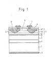
- an APD comprises an n-InP buffer layer 2 (about 1 micron thick), an n--In 0.53 G 0.43 As layer 3 (3.5 to 4.0 microns thick) of 3 to 5 x 10' 5 cm- 3 in carrier concentration, and an InGaAsP layer 3' (about 1 micron thick) having a bandgap corresponding to a wavelength of 1.3 microns, successively grown over a sulphur-doped n +- InP substrate 1.
- An n-InP layer 4 consists of an an-InP layer 41 (0.7 to 1.0 micron thick) of 3 to 4 x 10 16 cm- 3 in carrier concentration, an n - -InP layer 42 (about 1 micron thick) of 3 to 7 x 10" cm- 3 in carrier concentration, and an n -- -InP layer 43 (1 to 1.5 microns thick) of 1 to 2 x 10 15 cm- 3 in carrier concentration.
- the nlnP buffer layer 2 is intended to prevent any defect or dislocation in the InP substrate 1 from reaching the layers 3 to 43 during the process of layer growth; the n--lnGaAs layer 3, to absorb light of 1 to 1.7 microns in wavelength and generate positive hole and electron carriers; the n-InGaAsP layer 3', to prevent the traveling delay of the positive hole carriers due to the valence electron band discontinuity between the InP layer 4 and the InGaAs layer 3; and the n-InP layers 41 and 42 are avalanche multiplying layers.
- a p + type conductive region 5 (about 80 microns in diameter) selectively provided in a round or an oval shape as viewed from above and a guard-ring 5' (about 100 microns in outer diameter) provided in a ring shape around the circumference of the p + region 5.
- a p-electrode 7 is provided in a ring shape through a surface-protective film 6 with a selectively opened window in the p + type conductivity region 5, and an n-electrode 8 is formed all over the lower face of the substrate 1.
- the layers 2, 3, 3', 41, 42 and 43 were grown over the InP substrate 1, etched with a mixture of H 2 SO 4 , H 2 0 and H 2 0 2 in a 3:1:1 ratio, by the hydride vapor phase epitaxial method in a reactor - (not shown) combining an InP growth chamber, an InGaAsP growth chamber and an InGaAs growth chamber at a substrate temperature of 700°.C.
- the guard-ring was formed by implanting beryllium ions in the following process. Beryllium was used because it lends itself to the formation of a p-n junction closest to linear grading.
- An Si0 2 film was formed to a thickness of about 1 ⁇ m over the layer 43 by the pyrolitic chemical vapor phase deposition method - (thermal CVD method) at 370 ° C, and a window was selectively opened into said SiO 2 film with buffered fluoric acid solution by the use of an exposure mask for forming the guard-ring 5, on which a ring-shaped pattern was drawn by a usual light-exposure technique.
- beryllium ions were implanted within an accelerating voltage range of 100 to 140 KV and at a dose of 5 x 10 13 cm-2. At this time, the beryllium ions were implanted into the InP crystals, exposed by the opening selectively bored into the SiO 2 film.
- the SiO 2 film was removed by etching with the fluoric acid solution; then a phosphorated silica glass (PSG) layer was formed to a thickness of about 100 nm at 370°C by the thermal CVD method, and thermal treatment for activation and drive-in diffusion of the beryllium ions was conducted for about 20 minutes at 700°C, resulting in the formation of the guard-ring 5' in the illustrated shape.
- PSG phosphorated silica glass
- cadmium was thermally diffused within the guard-ring 5' for 20 to 30 minutes at a temperature of 570°C through the PSG film, into which a circular window had been selectively opened by the use of an exposure mask, to so form the p + type conductivity region 5 that the stepwise p t- n junction be positioned at the interface between the n - -InP layer 43 and the n - InP layer 42 or within the n - InP layer 42.
- the SiN surface-protective film 6 was plasma-deposited at 300°C to a thickness of 150 to 200 nm.
- a window was opened over the p + type conductive region 5 by the use of an exposure mask, on which a ring-shaped pattern had been drawn by a light-exposure technique, and the p-electrode 7 was formed by successively laying titanim, platinum and gold by the electron- bombardment evaporation method to thicknesses of 100 nm, 100 nm and 300 nm, respectively.
- the n-electrode 8 of AuGe/Ni alloy was formed all over the lower face of the substrate by the resistive heating evaporation method to finish the APD.
- a wafer having the same epitaxial structure was used to separately form a linearly graded p-n junction by beryllium ion implantation simultaneously with the aforementioned process.
- the breakdown voltage of this linearly graded p-n junction ranged from 120 to 150 V. That of the finished APD element was within the range of 100 to 110 V, lower than the 120 to 150 V range of the guard-ring section. Accordingly, avalanche multiplication of carriers was sufficiently achieved at the stepwise p +- n junction corresponding to the light receiving region surrounded by the ring-shaped p-electrode 7. This condition is illustrated in FIG. 2, where reference numeral 10 represents a typical multiplication sensitivity distribution, revealing that the carrier multiplication is greater in the stepwise p + -n junction corresponding to the light receiving region than in the guard-ring section.
- the APD according to the present invention is much less susceptible to noise than any prior art APD.
- a low-noise APD can be realized by increasing the difference between electrons' ionization rate a and positive holes' ⁇ .
- ⁇ is greater than ⁇ , so that noise can be reduced by enlarging the ⁇ / ⁇ ratio. Since the ⁇ / ⁇ ratio is a function of the electric field, and the lower the electric field, the greater the ⁇ / ⁇ ratio, noise can be reduced by lowering the electric field in the avalanche multiplying layer InP.
- the electric field is a function of the impurity concentration, and the lower the impurity concentration in the avalanche region, the lower the electric field, resulting in noise reduction.
- the excess noise factor (x-value) is expected to be somewhere between 0.5 and 0.6, representing a substantial improvement over the 0.7 to 0.8 of the prior art structure where the p +- n junction is positioned in a high impurity concentration layer.
- FIG. 3 shows a cross-sectional view of a second preferred embodiment of the present invention.
- the APD illustrated herein differs from the structure of FIG. 1 in that the impurity concentration of the n-InP layer 4 gradually decreases with the distance from the InGaAs light absorbing layer 3 and, consequently, in the shape of the guard-ring 5'. Since the two embodiments are alike in other respects, only these differences will be described in detail below.
- the n-lnP layer 4 has an impurity concentration of about 5 x 10' 6 cm -3 on its interface with the InGaAsP intermediate layer and an impurity concentration of approximately 1 x 10 15 cm- 3 at the uppermost level of the epitaxial structure, and the impurity concentration in-between gradually and continuously decreases toward the upper surface.
- the formation of the p + type conductivity region 5 is also achieved under the same conditions as those for the first preferred embodiment, the stepwise p + -n junction being positioned in an InP region whose impurity concentration is 3 to 5 x 10 15 c m -3.
- This preferred embodiment can be expected to give the same benefits as the first.
Landscapes
- Light Receiving Elements (AREA)
Applications Claiming Priority (4)
| Application Number | Priority Date | Filing Date | Title |
|---|---|---|---|
| JP60108634A JPS61265876A (ja) | 1985-05-20 | 1985-05-20 | プレ−ナ型ヘテロ接合半導体受光素子 |
| JP108634/85 | 1985-05-20 | ||
| JP60108661A JPS61267375A (ja) | 1985-05-21 | 1985-05-21 | プレ−ナ型ヘテロ接合半導体受光素子 |
| JP108661/85 | 1985-05-21 |
Publications (2)
| Publication Number | Publication Date |
|---|---|
| EP0205899A1 true EP0205899A1 (fr) | 1986-12-30 |
| EP0205899B1 EP0205899B1 (fr) | 1991-03-27 |
Family
ID=26448466
Family Applications (1)
| Application Number | Title | Priority Date | Filing Date |
|---|---|---|---|
| EP86106627A Expired - Lifetime EP0205899B1 (fr) | 1985-05-20 | 1986-05-15 | Photodiode à avalanche planaire à héterojonction |
Country Status (3)
| Country | Link |
|---|---|
| US (1) | US5057891A (fr) |
| EP (1) | EP0205899B1 (fr) |
| DE (1) | DE3678338D1 (fr) |
Cited By (3)
| Publication number | Priority date | Publication date | Assignee | Title |
|---|---|---|---|---|
| EP0304048A3 (fr) * | 1987-08-19 | 1990-05-23 | Nec Corporation | Photodiode planaire à avalanche à hétérojonction |
| EP0347157A3 (fr) * | 1988-06-17 | 1990-06-06 | Nec Corporation | Dispositif récepteur de lumière à semiconducteur PIN |
| US8198650B2 (en) | 2008-12-08 | 2012-06-12 | General Electric Company | Semiconductor devices and systems |
Families Citing this family (11)
| Publication number | Priority date | Publication date | Assignee | Title |
|---|---|---|---|---|
| JPH04111478A (ja) * | 1990-08-31 | 1992-04-13 | Sumitomo Electric Ind Ltd | 受光素子 |
| JPH0777271B2 (ja) * | 1992-12-04 | 1995-08-16 | 日本電気株式会社 | アバランシェフォトダイオード |
| US5610416A (en) * | 1995-02-16 | 1997-03-11 | Hewlett-Packard Company | Avalanche photodiode with epitaxially regrown guard rings |
| KR19980058393A (ko) * | 1996-12-30 | 1998-10-07 | 김영환 | 애벌런치 포토 다이오드 및 그의 제조방법 |
| US5866936A (en) * | 1997-04-01 | 1999-02-02 | Hewlett-Packard Company | Mesa-structure avalanche photodiode having a buried epitaxial junction |
| US6583482B2 (en) * | 2000-12-06 | 2003-06-24 | Alexandre Pauchard | Hetero-interface avalance photodetector |
| JP3910817B2 (ja) * | 2000-12-19 | 2007-04-25 | ユーディナデバイス株式会社 | 半導体受光装置 |
| JP2002231992A (ja) * | 2001-02-02 | 2002-08-16 | Toshiba Corp | 半導体受光素子 |
| DE102004022948B4 (de) * | 2004-05-10 | 2006-06-01 | MAX-PLANCK-Gesellschaft zur Förderung der Wissenschaften e.V. | Avalanche-Strahlungsdetektor |
| US7147270B1 (en) * | 2005-05-13 | 2006-12-12 | Paul Guy Andrus | Automatic rear airfoil for vehicle |
| WO2019211968A1 (fr) * | 2018-05-02 | 2019-11-07 | ソニーセミコンダクタソリューションズ株式会社 | Élément de capture d'image à semi-conducteur et dispositif de capture d'image |
Family Cites Families (3)
| Publication number | Priority date | Publication date | Assignee | Title |
|---|---|---|---|---|
| US4383266A (en) * | 1979-09-26 | 1983-05-10 | Kokusai Denshin Denwa Kabushiki Kaisha | Avalanche photo diode |
| JPS6016474A (ja) * | 1983-07-08 | 1985-01-28 | Nec Corp | ヘテロ多重接合型光検出器 |
| US4651187A (en) * | 1984-03-22 | 1987-03-17 | Nec Corporation | Avalanche photodiode |
-
1986
- 1986-05-15 EP EP86106627A patent/EP0205899B1/fr not_active Expired - Lifetime
- 1986-05-15 DE DE8686106627T patent/DE3678338D1/de not_active Expired - Lifetime
-
1991
- 1991-02-12 US US07/653,487 patent/US5057891A/en not_active Expired - Lifetime
Non-Patent Citations (6)
| Title |
|---|
| ELECTRONICS LETTERS, vol. 17, no. 22, October 1981, pages 826,827, London, GB; T. SHIRAI et al.: "1.3 mum InP/InGaAsP planar avalanche photodiodes" * |
| ELECTRONICS LETTERS, vol. 18, no. 13, June 1982, pages 575-577, London, GB; T. SHIRAI et al.: "1.0-1.6 mum planar avalanche photodiode by LPE grown Inp/InGaAs/InP DH structure" * |
| ELECTRONICS LETTERS, vol. 19, no. 14, July 1983, pages 534-536, London, GB; T. SHIRAI et al.: "InGaAs avalanche photodiodes for 1 mum wavelength region" * |
| ELECTRONICS LETTERS, vol. 20, no. 24, November 1984, pages 993,994, London, GB; N. NIWA et al.: "Receiver sensitivity temperature dependence of small detectable area Hi-Lo germanium avalanche photodiode" * |
| PATENTS ABSTRACTS OF JAPAN, vol. 7, no. 132 (E-180)[1277], 9th June 1983; JP-A-58 048 478 (FUJITSU K.K.) 22-03-1983 * |
| TENTH EUROPEAN CONFERENCE ON OPTICAL COMMUNICATION, Stuttgart, DE, 3rd-6th September 1984, pages 220,221, Amsterdam, NL; T. TORIKAI et al.: "Low noise and high speed InP/InGaAsP/InGaAs avalanche photodiodes with planar structure grown by vapor phase epitaxy" * |
Cited By (4)
| Publication number | Priority date | Publication date | Assignee | Title |
|---|---|---|---|---|
| EP0304048A3 (fr) * | 1987-08-19 | 1990-05-23 | Nec Corporation | Photodiode planaire à avalanche à hétérojonction |
| US4974061A (en) * | 1987-08-19 | 1990-11-27 | Nec Corporation | Planar type heterostructure avalanche photodiode |
| EP0347157A3 (fr) * | 1988-06-17 | 1990-06-06 | Nec Corporation | Dispositif récepteur de lumière à semiconducteur PIN |
| US8198650B2 (en) | 2008-12-08 | 2012-06-12 | General Electric Company | Semiconductor devices and systems |
Also Published As
| Publication number | Publication date |
|---|---|
| US5057891A (en) | 1991-10-15 |
| DE3678338D1 (de) | 1991-05-02 |
| EP0205899B1 (fr) | 1991-03-27 |
Similar Documents
| Publication | Publication Date | Title |
|---|---|---|
| EP0159544B1 (fr) | Photodiode à avalanche et méthode pour sa fabrication | |
| EP0053513B1 (fr) | Photodiodes à avalanche | |
| US5144381A (en) | Semiconductor light detector utilizing an avalanche effect and having an improved guard ring structure | |
| US5157473A (en) | Avalanche photodiode having guard ring | |
| EP0869561B1 (fr) | Photodiode à avalanche et son procédé de fabrication | |
| US5843804A (en) | Method of making avalanche photodiodes with epitaxially-regrown guard rings | |
| US7345325B2 (en) | Avalanche photodiode | |
| US4442444A (en) | Avalanche photodiodes | |
| EP0205899B1 (fr) | Photodiode à avalanche planaire à héterojonction | |
| EP0216572A2 (fr) | Photodétecteur à semi-conducteur ayant un profil d'impureté à deux échelons | |
| EP0163546B1 (fr) | Procédé pour fabriquer une photodiode à avalanche et photodiode ainsi obtenue | |
| CA2007670C (fr) | Photodetecteur semiconducteur et methode de fabrication de ce photodetecteur | |
| GB1594246A (en) | Semiconductor device having a passivating layer | |
| KR910009357B1 (ko) | 반도체 포토-다이오드 | |
| EP0304048B1 (fr) | Photodiode planaire à avalanche à hétérojonction | |
| CA1203877A (fr) | Methode de fabrication de photodiodes planar a heterostructure | |
| KR970009732B1 (ko) | 평면형 광검출기의 제조방법 | |
| KR0175441B1 (ko) | 애벌랜치 포토다이오드의 제조방법 | |
| KR0164094B1 (ko) | 부분적으로 높은 전하층을 갖는 애벌랜치 포토다이오드 및 그의 제조방법 | |
| JPS60173882A (ja) | 半導体装置 | |
| JPS61265876A (ja) | プレ−ナ型ヘテロ接合半導体受光素子 | |
| JPH02253666A (ja) | 半導体受光素子 | |
| JPH0738137A (ja) | 半導体受光素子およびその製造方法と光電子集積回路 | |
| JPH03201489A (ja) | 半導体受光素子 | |
| JPS60260167A (ja) | 半導体受光装置 |
Legal Events
| Date | Code | Title | Description |
|---|---|---|---|
| PUAI | Public reference made under article 153(3) epc to a published international application that has entered the european phase |
Free format text: ORIGINAL CODE: 0009012 |
|
| 17P | Request for examination filed |
Effective date: 19860515 |
|
| AK | Designated contracting states |
Kind code of ref document: A1 Designated state(s): DE FR GB |
|
| ITCL | It: translation for ep claims filed |
Representative=s name: BARZANO' E ZANARDO ROMA S.P.A. |
|
| 17Q | First examination report despatched |
Effective date: 19881031 |
|
| GRAA | (expected) grant |
Free format text: ORIGINAL CODE: 0009210 |
|
| AK | Designated contracting states |
Kind code of ref document: B1 Designated state(s): DE FR GB |
|
| ET | Fr: translation filed | ||
| REF | Corresponds to: |
Ref document number: 3678338 Country of ref document: DE Date of ref document: 19910502 |
|
| PLBE | No opposition filed within time limit |
Free format text: ORIGINAL CODE: 0009261 |
|
| STAA | Information on the status of an ep patent application or granted ep patent |
Free format text: STATUS: NO OPPOSITION FILED WITHIN TIME LIMIT |
|
| 26N | No opposition filed | ||
| REG | Reference to a national code |
Ref country code: GB Ref legal event code: IF02 |
|
| PGFP | Annual fee paid to national office [announced via postgrant information from national office to epo] |
Ref country code: GB Payment date: 20050511 Year of fee payment: 20 Ref country code: FR Payment date: 20050511 Year of fee payment: 20 |
|
| PGFP | Annual fee paid to national office [announced via postgrant information from national office to epo] |
Ref country code: DE Payment date: 20050512 Year of fee payment: 20 |
|
| REG | Reference to a national code |
Ref country code: GB Ref legal event code: PE20 |
|
| PG25 | Lapsed in a contracting state [announced via postgrant information from national office to epo] |
Ref country code: GB Free format text: LAPSE BECAUSE OF EXPIRATION OF PROTECTION Effective date: 20060514 |