EP0209194B1 - Procédé de fabrication d'un dispositif semi-conducteur, comportant l'attaque chimique d'une couche de Ga-As à l'aide d'une solution alcaline de peroxyde d'hydrogène - Google Patents
Procédé de fabrication d'un dispositif semi-conducteur, comportant l'attaque chimique d'une couche de Ga-As à l'aide d'une solution alcaline de peroxyde d'hydrogène Download PDFInfo
- Publication number
- EP0209194B1 EP0209194B1 EP86201220A EP86201220A EP0209194B1 EP 0209194 B1 EP0209194 B1 EP 0209194B1 EP 86201220 A EP86201220 A EP 86201220A EP 86201220 A EP86201220 A EP 86201220A EP 0209194 B1 EP0209194 B1 EP 0209194B1
- Authority
- EP
- European Patent Office
- Prior art keywords
- layer
- etched
- groove
- gallium arsenide
- solution
- Prior art date
- Legal status (The legal status is an assumption and is not a legal conclusion. Google has not performed a legal analysis and makes no representation as to the accuracy of the status listed.)
- Expired
Links
Images
Classifications
-
- H—ELECTRICITY
- H10—SEMICONDUCTOR DEVICES; ELECTRIC SOLID-STATE DEVICES NOT OTHERWISE PROVIDED FOR
- H10P—GENERIC PROCESSES OR APPARATUS FOR THE MANUFACTURE OR TREATMENT OF DEVICES COVERED BY CLASS H10
- H10P50/00—Etching of wafers, substrates or parts of devices
- H10P50/60—Wet etching
- H10P50/64—Wet etching of semiconductor materials
- H10P50/642—Chemical etching
- H10P50/646—Chemical etching of Group III-V materials
- H10P50/648—Anisotropic liquid etching
Definitions
- the invention relates to a method of manufacturing a semiconductor device, in which a photolacquer mask is provided on a (001) or equivalently orientated surface of a monocrystalline layer of gallium arsenide, after which the layer is etched in a basic solution of hydrogen peroxide.
- (001) or equivalently orientated surface is to be understood herein to mean a surface which extends parallel to one of the crystal surfaces (001), (010) and (100) of the monocrystalline layer of gallium arsenide.
- an epitaxial layer of gallium arsenide can be etched with a high selectivity with respect to a layer of gallium aluminium arsenide.
- a high etching selectivity is very desirable, for example, in the manufacture of semiconductor lasers or laser diodes.
- Such a preferential etching behaviour of an etching solution means that the method mentioned in the opening paragraph is suitable only for the manufacture of a very limited number of semiconductor devices.
- the invention has inter alia for its object to considerably enlarge the usability of the method by enlarging the usability of the etching solution.
- the method of the kind mentioned in the opening paragraph is for this purpose characterized in that the layer is etched in a solution having an acidity which is determined in such a manner that, when a groove extending parallel to a [110] or equivalent direction is etched in the layer, this groove has a V-shaped cross-section.
- a [110] or equivalent direction is to be understood herein to mean the [110] direction when the groove is etched in a (001)-orientated surface, the [011] direction when this is the case in a (100)-orientated surface and the [101] direction when this is the case in a (010)-orientated surface, that is to say in each of the possible orientations of the layer of gallium arsenide that direction which corresponds to the [110] direction with a layer having a (001)-orientated surface.
- a V-shaped groove is to be understood to mean a groove which tapers in do wnward direction, in contrast with a dovetail-shaped groove, which widens in downward direction.
- a groove having a V-shaped cross-section can be etched in a direction which is transverse to that in which a groove having a V-shaped cross-section is obtained with the known strong basic etching solution.
- the V-shaped groove extended in the [ 1 10] direction.
- a dovetail-shaped groove can be obtained by means of the method according to the invention.
- a preferred embodiment of the method according to the invention is characterized in that the acidity of the solution is determined in such a manner that, when at the same time a groove extending parallel to a [ 1 10] or equivalent direction is etched in the layer, this groove also has a V-shaped cross-section.
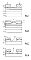
- Figures 1 and 2 show diagrammatically and in cross-section a few stages of the manufacture of a semi-conductor laser obtained by means of the method according to the invention
- Figures 3 and 4 show shapes of grooves obtained during etching of a (001)-orientated layer of gallium arsenide in the [110] and the [ 1 10] direction, respectively.
- Figures 1 and 2 show diagrammatically and in cross-section a few stages of the manufacture of a semi-conductor laser obtained by means of the method according to the invention.
- an about 2 ⁇ m thick n -type layer of gallium arsenide 3 having a doping concentration of about 1018 atoms/cm3 an about 2 ⁇ m thick layer of gallium aluminium arsenide 4 having a composition Ga 0.65 Al 0.35 As and a doping concentration of about 1018 atoms/cm3, an about 0.1 ⁇ m thick so-called active undoped layer of gallium arsenide 5, an about 0.4 ⁇ m thick p -type of gallium aluminium arsenide 6 having a composition Ga 0.65 Al 0.35 As and a doping concentration of about 5.1017 atoms/cm3 and an about 0.5 ⁇ m thick n -type layer of gallium arsenide 7 having a doping concentration of about 3.1018 atoms/cm3 are successively formed by means of liquid
- the layer of gallium arsenide 7 has a surface 8 which also extends parallel to (001) crystal surfaces; consequently, this surface 8 is also (001)-orientated.
- the starting material was a (001)-orientated substrate 2 with a (001)-orientated layer 7 of gallium arsenide, but a similar situation had been possible by starting from a (010)-or a (100)-orientated substrate and gallium arsenide layer.
- a photolacquer mask 9 is provided on the (001)-orientated surface 8 of the monocrystalline layer 7 of gallium arsenide, after which the layer is etched in a basic solution of hydrogen peroxide.
- the layer 7 of gallium arsenide can be etched with a high selectivity with respect to the layer 6 of gallium aluminium arsenide.
- an about 5 ⁇ m wide groove 10 directed at right angles to the plane of the drawing is etched into the layer 7 of gallium arsenide.
- the layer 6 of gallium aluminium arsenide is then practically not attacked.
- the layer 7 of gallium arsenide is etched in a solution having an acidity (pH) which is determined so that, when a groove extending parallel to a [110] or equivalent direction is etched into the layer 7 of gallium arsenide, this groove has a V-shaped cross-section.
- a [110] or equivalent direction has to be understood to mean that for a (001)-orientated surface 8 the [110] direction is meant and for a (100) - and a (010)-orientated surface 8 the [011]and the [101] direction, respectively, are meant.
- the groove 10 extends in the [110] direction and the groove 10 has a V-shaped cross-section.
- V-shaped cross-section is to be understood to mean a cross-section which tapers in downward direction.
- the photolacquer mask 9 is removed and an about 2 ⁇ m thick p -type layer 11 of gallium aluminium arsenide having a doping concentration of about 5.1017 atoms/cm3 and an about 0.2 ⁇ m thick p -type gallium arsenide contact layer 12 are formed successively in a usual manner by means of an epitaxial growing process from a gas mixture of metal-organic gases (MOCVD).
- MOCVD metal-organic gases
- the groove 10 defines the area at which the current flows through the laser and at which consequently the laser light is generated in the active layer 5.
- Figures 3 and 4 show a layer 20 of gallium aluminium arsenide, on which a monocrystalline layer 21 of gallium arsenide is formed, which is covered with a photolacquer mask 22.
- the layer 21 of galliumarsenide is (001)-orientated; in Fig. 3, the [110] direction extends at right angles to the plane of the drawing, while in Fig. 4 the [ 1 10] direction extends at right angles to this plane.
- a groove 23 having a V-shaped cross-section is etched in the [110] direction and a groove 24 having a dovetail-shaped cross-section is etched in the [ 1 10] direction; that is to say that the width of this groove decreases (23) and increases (24), respectively, in downward direction.
- the acidity has to be comparatively low (pH ⁇ 8.2).
- the acidity is adjusted so as to be comparatively high (pH>9), quite different grooves are obtained; the groove extending in the [110] direction then has a dovetail-shaped cross-section, while the groove extending in the [ 1 10] direction has a V-shaped cross-section.
- the V-shaped groove which is etched with a strong basic solution (pH>9), has flat surfaces constituted by ( 11 1) surfaces, which are occupied by gallium atoms; the V-shaped groove, which is etched with a comparatively weak basic solution (pH ⁇ 8.2), has slightly curved walls, which contain a comparatively large number of arsenic atoms. This is of great importance if by means of a growing process from a gas mixture of metal-organic constituents (MOCVD) a layer has to be provided. Deposition on a surface containing a comparatively large number of arsenic atoms is effected in a much simpler manner than on a surface containing only gallium atoms. This is due to the fact that gallium oxides are much more stable than arsenic oxides and are broken down only slowly during the deposition process, which is effected at a comparatively low temperature, while arsenic oxides then evaporate.
- the acidity of the solution is determined so that, when a groove is etched in the [ 1 10] direction into the layer 7,21 of galliumarsenide, this groove, like a groove in the [110] direction, has a V-shaped cross-section.
- the acidity then lies in the range of from 7.80 to 8.25.
- a (001)-orientated undoped layer of gallium arsenide was etched at room temperature in a 30% solution of hydrogen peroxide. Different substances were added to this solution inter alia for determining the acidity.
- the gallium arsenide layer was provided with a photolacquer mask, which was provided with slot-shaped openings so that it was possible to etch grooves into the gallium arsenide layer both in the [110] direction and in the [ 1 10] direction.
- a V-shaped groove is designated by V and a dovetail-shaped groove is designated by Z.
- a V-shaped groove is obtained in the [110] direction and when etching in a solution having a pH of 7.80 to 8.25, a V-shaped groove is obtained both in the [110] direction and in the [ 1 10] direction.
- the shape of the etched groove does not change abruptly in the embodiment described above from the V-form to the dovetail form.
- the mixed forms having a V-shaped character are designated in the tables by V and the mixed forms having a dovetail character are designated therein by Z.
- the acidity of the etching solution may be determined by other bases, such as, for example, potassium hydroxide. In all these cases, corresponding results are obtained.
- a weak acid may also be added to the etching solution, after which the acidity is adjusted by a base. If, for example, perchloric acid is added as acid and if then the acidity is adjusted by means of ammonia, the etching process is effected more rapidly than in a solution having the same acidity, to which only ammonia is added.
Landscapes
- Weting (AREA)
Claims (2)
- Procédé de fabrication d'un dispositif semiconducteur dans lequel un photomasque en vernis est respectivement prévu sur une face orientée suivant (001) , (100) ou (010) d'une couche monocristalline d'arséniure de gallium et est pourvu d'ouvertures s'étendant parallèlement aux directions [110], [011] ou [101] respectivement, après quoi ladite couche est soumise à une morsure dans une solution alcaline de peroxyde d'hydrogène, caractérisé en ce que l'acidité de la solution (pH) est inférieure à 8,25, de sorte que des rainures s'étendant parallèlement à la direction [100], [011] ou [101] respectivement sont formées dans la couche avec une section transversale en V.
- Procédé suivant la revendication 1, caractérisé en ce que l'acidité (pH) de la solution est de 7,8 à 8,25, de sorte que, lors de la formation par morsure, dans ladite couche, d'une rainure qui s'étend parallèlement à une direction [
1 10], [01 1] ou [1 01] respectivement, cette rainure a également une section transversale en V.
Applications Claiming Priority (2)
| Application Number | Priority Date | Filing Date | Title |
|---|---|---|---|
| NL8502022 | 1985-07-15 | ||
| NL8502022 | 1985-07-15 |
Publications (2)
| Publication Number | Publication Date |
|---|---|
| EP0209194A1 EP0209194A1 (fr) | 1987-01-21 |
| EP0209194B1 true EP0209194B1 (fr) | 1991-04-17 |
Family
ID=19846297
Family Applications (1)
| Application Number | Title | Priority Date | Filing Date |
|---|---|---|---|
| EP86201220A Expired EP0209194B1 (fr) | 1985-07-15 | 1986-07-14 | Procédé de fabrication d'un dispositif semi-conducteur, comportant l'attaque chimique d'une couche de Ga-As à l'aide d'une solution alcaline de peroxyde d'hydrogène |
Country Status (3)
| Country | Link |
|---|---|
| EP (1) | EP0209194B1 (fr) |
| JP (1) | JP2641194B2 (fr) |
| DE (1) | DE3678761D1 (fr) |
Families Citing this family (5)
| Publication number | Priority date | Publication date | Assignee | Title |
|---|---|---|---|---|
| JPS6158273A (ja) * | 1984-08-29 | 1986-03-25 | Hitachi Ltd | 化合物半導体メサ状構造体 |
| JPS6457786A (en) * | 1987-08-28 | 1989-03-06 | Mitsubishi Electric Corp | Manufacture of semiconductor laser device |
| DE3920644C1 (fr) * | 1989-06-23 | 1990-12-20 | Fraunhofer-Gesellschaft Zur Foerderung Der Angewandten Forschung Ev, 8000 Muenchen, De | |
| JP2010050204A (ja) * | 2008-08-20 | 2010-03-04 | Oki Semiconductor Co Ltd | 半導体素子の製造方法 |
| EP3040777B1 (fr) | 2013-08-28 | 2018-03-14 | Nissan Chemical Industries, Ltd. | Procédé de formation de motif à l'aide d'un film de sous-couche de réserve |
Family Cites Families (5)
| Publication number | Priority date | Publication date | Assignee | Title |
|---|---|---|---|---|
| FR2168936B1 (fr) * | 1972-01-27 | 1977-04-01 | Labo Electronique Physique | |
| US3801391A (en) * | 1972-09-25 | 1974-04-02 | Bell Telephone Labor Inc | Method for selectively etching alxga1-xas multiplier structures |
| JPS5228873A (en) * | 1975-08-29 | 1977-03-04 | Agency Of Ind Science & Technol | Method for production of the cubic structure consisting of the semicon ductive crystal and the semiconductive device made of it's cubic struc ture |
| FR2486104A1 (fr) * | 1980-07-04 | 1982-01-08 | Radiotechnique Compelec | Procede d'obtention de creusures a contour circulaire dans les monocristaux de composes intermetalliques cristallisant dans le systeme cubique a faces centrees et dispositif comportant de telles creusures |
| US4623427A (en) * | 1983-08-12 | 1986-11-18 | Hewlett-Packard Company | Means and method for a self-aligned multilayer laser epitaxy structure device |
-
1986
- 1986-07-14 JP JP61163908A patent/JP2641194B2/ja not_active Expired - Lifetime
- 1986-07-14 DE DE8686201220T patent/DE3678761D1/de not_active Expired - Lifetime
- 1986-07-14 EP EP86201220A patent/EP0209194B1/fr not_active Expired
Also Published As
| Publication number | Publication date |
|---|---|
| JPS6220326A (ja) | 1987-01-28 |
| JP2641194B2 (ja) | 1997-08-13 |
| DE3678761D1 (de) | 1991-05-23 |
| EP0209194A1 (fr) | 1987-01-21 |
Similar Documents
| Publication | Publication Date | Title |
|---|---|---|
| JP4802556B2 (ja) | チップ状電子部品の製造方法 | |
| US3887404A (en) | Method of manufacturing semiconductor devices | |
| GB2101045A (en) | Method of etching optically flat facets in ingaasp/ inp heterostructures | |
| US5093278A (en) | Method of manufacturing a semiconductor laser | |
| JPH0673390B2 (ja) | 埋め込みヘテロ構造半導体デバイスの製作方法 | |
| US5266518A (en) | Method of manufacturing a semiconductor body comprising a mesa | |
| EP0815585B1 (fr) | Attaque selective d'un substrat semi-conducteur par rapport aux couches epitaxiales | |
| US5242857A (en) | Method of manufacturing semiconductor structures | |
| EP0209194B1 (fr) | Procédé de fabrication d'un dispositif semi-conducteur, comportant l'attaque chimique d'une couche de Ga-As à l'aide d'une solution alcaline de peroxyde d'hydrogène | |
| US4049488A (en) | Method of manufacturing a semiconductor device | |
| Samid et al. | Embedded heterostructure epitaxy: A technique for two‐dimensional thin‐film definition | |
| JP3097863B2 (ja) | AlGaAs自然酸化物 | |
| EP0414457B1 (fr) | Procédé d'attaque sélective | |
| Yu et al. | Anodic oxidation of Al x Ga1− x As | |
| JPS5881973A (ja) | 金−ゲルマニウム合金膜のエツチング方法 | |
| JPS6223191A (ja) | リツジ型半導体レ−ザ装置の製造方法 | |
| Huo et al. | New chemical solutions for the etching of (011) oriented V-grooves in InP (001) for CSBH laser diodes | |
| JPH0415616B2 (fr) | ||
| JPS6366414B2 (fr) | ||
| JPH01316471A (ja) | エッチング液 | |
| JPS61272990A (ja) | 半導体レ−ザ | |
| JP2005072623A (ja) | 半導体素子 | |
| JPH10189557A (ja) | 化合物半導体のエッチング方法 | |
| KR19990024760A (ko) | 양자세선 제조 방법 | |
| JPH07183286A (ja) | AlGaAs半導体層のエッチング方法 |
Legal Events
| Date | Code | Title | Description |
|---|---|---|---|
| PUAI | Public reference made under article 153(3) epc to a published international application that has entered the european phase |
Free format text: ORIGINAL CODE: 0009012 |
|
| AK | Designated contracting states |
Kind code of ref document: A1 Designated state(s): DE FR GB NL |
|
| 17P | Request for examination filed |
Effective date: 19870525 |
|
| 17Q | First examination report despatched |
Effective date: 19890424 |
|
| GRAA | (expected) grant |
Free format text: ORIGINAL CODE: 0009210 |
|
| AK | Designated contracting states |
Kind code of ref document: B1 Designated state(s): DE FR GB NL |
|
| REF | Corresponds to: |
Ref document number: 3678761 Country of ref document: DE Date of ref document: 19910523 |
|
| ET | Fr: translation filed | ||
| PG25 | Lapsed in a contracting state [announced via postgrant information from national office to epo] |
Ref country code: NL Effective date: 19920201 |
|
| PLBE | No opposition filed within time limit |
Free format text: ORIGINAL CODE: 0009261 |
|
| STAA | Information on the status of an ep patent application or granted ep patent |
Free format text: STATUS: NO OPPOSITION FILED WITHIN TIME LIMIT |
|
| NLV4 | Nl: lapsed or anulled due to non-payment of the annual fee | ||
| 26N | No opposition filed | ||
| REG | Reference to a national code |
Ref country code: FR Ref legal event code: CD |
|
| PGFP | Annual fee paid to national office [announced via postgrant information from national office to epo] |
Ref country code: GB Payment date: 19980701 Year of fee payment: 13 |
|
| PGFP | Annual fee paid to national office [announced via postgrant information from national office to epo] |
Ref country code: FR Payment date: 19980716 Year of fee payment: 13 |
|
| REG | Reference to a national code |
Ref country code: FR Ref legal event code: CD |
|
| PG25 | Lapsed in a contracting state [announced via postgrant information from national office to epo] |
Ref country code: GB Free format text: LAPSE BECAUSE OF NON-PAYMENT OF DUE FEES Effective date: 19990714 |
|
| PG25 | Lapsed in a contracting state [announced via postgrant information from national office to epo] |
Ref country code: FR Free format text: THE PATENT HAS BEEN ANNULLED BY A DECISION OF A NATIONAL AUTHORITY Effective date: 19990731 |
|
| GBPC | Gb: european patent ceased through non-payment of renewal fee |
Effective date: 19990714 |
|
| REG | Reference to a national code |
Ref country code: FR Ref legal event code: ST |
|
| PGFP | Annual fee paid to national office [announced via postgrant information from national office to epo] |
Ref country code: DE Payment date: 20030731 Year of fee payment: 18 |
|
| PG25 | Lapsed in a contracting state [announced via postgrant information from national office to epo] |
Ref country code: DE Free format text: LAPSE BECAUSE OF NON-PAYMENT OF DUE FEES Effective date: 20050201 |