EP0211674A2 - Dispositif de sélection et protection du signal d'horloge - Google Patents
Dispositif de sélection et protection du signal d'horloge Download PDFInfo
- Publication number
- EP0211674A2 EP0211674A2 EP86306167A EP86306167A EP0211674A2 EP 0211674 A2 EP0211674 A2 EP 0211674A2 EP 86306167 A EP86306167 A EP 86306167A EP 86306167 A EP86306167 A EP 86306167A EP 0211674 A2 EP0211674 A2 EP 0211674A2
- Authority
- EP
- European Patent Office
- Prior art keywords
- clock
- signal
- input
- clock signal
- output
- Prior art date
- Legal status (The legal status is an assumption and is not a legal conclusion. Google has not performed a legal analysis and makes no representation as to the accuracy of the status listed.)
- Withdrawn
Links
Images


Classifications
-
- H—ELECTRICITY
- H04—ELECTRIC COMMUNICATION TECHNIQUE
- H04L—TRANSMISSION OF DIGITAL INFORMATION, e.g. TELEGRAPHIC COMMUNICATION
- H04L7/00—Arrangements for synchronising receiver with transmitter
- H04L7/0079—Receiver details
- H04L7/0083—Receiver details taking measures against momentary loss of synchronisation, e.g. inhibiting the synchronisation, using idle words or using redundant clocks
Definitions
- the present invention relates to clock signal selection and security arrangements and more particularly but not exclusively to such arrangements for use in a time-division-multiplexed pulse-code- modulated digital signal switching system.
- a clock signal security arrangement comprising inputs for at least three corresponding clock signals, averaging means arranged to provide a comparison clock signal derived from all of the clock input signals, and comparison means arranged to compare each input clock signal with said comparison clock signal, said comparison means providing an output signal in dependance upon the validity of each of said clock input signals.
- said arrangement also comprises delay means arranged to provide a delayed clock signal derived from said comparison clock signal, and said comparison means is enabled when both said delayed clock signal and said comparison clock signal are at the same value the delay being selected such that comparison of the input clock signals with the comparison clock signal occurs substantially mid-way through a pulse period of the comparison clock signal.
- the comparison clock signal is selected for output as a controlling clock signal.
- one of the input clock signals is selected for output as a controlling clock signal in dependance upon the output of the comparison means.
- an input clock signal present on a first input is selected for output as the controlling clock signal unless said clock signal is determined as faulty by the comparison means. If the clock signal present on said first input is determined as faulty by satd comparison means the clock signal on a second input is selected for output as the controlling clock signal.
- the selection of the controlling signal may be by a circuit comprising a first logic gate which receives the first clock input signal, and a second logic gate which receives the second clock input signal, said first logic gate outputting either the first clock input signal or an enable signal to said second logic gate in dependance upon the output of the comparison means, said second logic gate passing either the first clock signal or the second clock signal.
- the comparison means may be arranged to output a signal to control means indicating the presence of a fault in one of the input clock signals to provide an interrupt signal to such control means.
- a data signal indicating which of the input clock signals is faulty may be output in parallel with said interrupt signal.
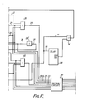
- the system accepts three levels of each of two clocks from a telecommunications exchange clock generation system (not shown).
- the first clock at 2048 kilohertz is received on inputs 1,2 and 3 whilst the second clock, an eight kilohertz time-division-multiplex - (TDM) frame synchronisation signal is received on inputs 41,42 and 43.
- TDM time-division-multiplex -
- An adder circuit 10 performs a two out of three majority decision on the three clock levels which majority decision is distributed by a connection 11 to various fault detection elements of the circuit.
- the majority decision clock is not used as the master clock signal to be supplied since if a fault is present an uneven mark/space ratio may be generated if skew due to differential input delays is present in one or both of the two majority clocks.
- the majority decision clock is used as a comparison signal in the fault detection circuitry which comprises three comparison gates 17,18,19 whence the clock signals on connections 7,8 and 9 are respectively fed by way of respective bistable elements in a circuit 12 via respective connections on leads 14,15,16.
- the majority clock on lead 11 is fed by way of a respective bistable element in the circuit 12 on a connection 13 to the other inputs of each of the comparison gates 17,18,19.
- the signal from the first clock comparison gate 17 is inverted by a NOR gate 28' to provide an enable signal via connection 27 to enable a gate 25 which is also enabled by the signal on the connection 21 from the gate 18 if the second clock signal from the input 2 is satisfactory.
- the clock signal on connection 8 is enabled through the gate 25 and the gate 24 to provide the master clock on the lead 26.
- the output signal from the gate 28' via the connection 27 disables the gate 25 to prevent the passage of the clock signal received on the input 2 to the output lead 26. It may be seen therefore that if the clock on the input 1 is satisfactory it acts as the master clock regardless of the condition of the clock on the input 2. However, if the clock on the input 1 is determined as faulty, the clock on the input 2 acts as the master clock.
- the clock provided on the input 3 serves only as an arbiter for the majority decision logic and is not selected for output.
- any of the three clocks on the inputs 1,2 or 3 is determined as faulty, it is necessary for an alarm condition to be generated. This is achieved by combining the three clock condition signals from the gates 17, 18 and 19 in a gate 28 which outputs a signal on connection 29 if any fault output is present. This signal passes by way of a bistable circuit in a logic circuit 30 to a NAND gate 31 which, if either input changes, forwards an interrupt signal on a lead 32 to the exchange control system (not shown) indicating a clock failure.
- an indication of the presence of a clock fault is output through a multiplexer contained in a circuit 33 together with an indication of which clock is at fault output through three other multiplexers either in the circuit 33 or in a circuit 34 to data leads 35-38.
- the function of the other multiplexer inputs will become apparent from the description which follows relating to the second group of clocks.
- clocking of the bistable circuit 12 to effect comparison of the clocks is derived from the average clock on connection 11 from the adder 10 by way of a delay circuit 39 and a gate 40.
- the delay is selected to be approximately 120 nano seconds incorporated in a commercially available selectable delay circuit. This ensures that comparison of the clock signals occurs after the input clock transitions.
- the three levels of frame synchronisation clock are received on inputs 41,42 and 43 and pass via receivers 44,45 and 46 and connections 47,48 and 49 to the adder circuit 10. In this case the output of the adder circuit 10. a two out of three majority signal is fed directly to output 50 for use as the system frame synchronisation signal.
- This average clock on connection 50 together with the three clock signals received now passes by way of a respective bistable circuit 52 and connection 53 to three comparison gates 57,58,59 which, in the same manner as the gates 17,18,19 determines whether any of the three clock signals are faulty. If one of the clocks is determined as faulty a NOR gate 60 connected to a respective bistable element in the circuit 30 causes the output of an interrupt signal by way of NAND gate 31 and lead 32 in the same manner as the main clock signal.
- a clock fault indication is provided through the first four to one multiplexer circuit in element 33 to the data output 35 with an indication of the faulty clock through respective multiplexers of elements 33 and 34 to data outputs 36,37 and 38.
- bistable circuit 52 is clocked from the two megahertz main clock signal. It will also be noted that the unconnected inputs of the multiplexers of elements 33 and 34 are available for other fault reporting circuits such as pcm speech paths (not shown).
- a reset signal may be applied to lead 61 connected to the bistable elements 12,52 to clear any fault indications occurring on (eg.) intiatisation of a connected system.
Landscapes
- Engineering & Computer Science (AREA)
- Computer Networks & Wireless Communication (AREA)
- Signal Processing (AREA)
- Synchronisation In Digital Transmission Systems (AREA)
- Time-Division Multiplex Systems (AREA)
Applications Claiming Priority (2)
| Application Number | Priority Date | Filing Date | Title |
|---|---|---|---|
| GB08520035A GB2178926A (en) | 1985-08-09 | 1985-08-09 | Clock signal selection and security arrangements |
| GB8520035 | 1985-08-09 |
Publications (2)
| Publication Number | Publication Date |
|---|---|
| EP0211674A2 true EP0211674A2 (fr) | 1987-02-25 |
| EP0211674A3 EP0211674A3 (fr) | 1989-01-18 |
Family
ID=10583551
Family Applications (1)
| Application Number | Title | Priority Date | Filing Date |
|---|---|---|---|
| EP86306167A Withdrawn EP0211674A3 (fr) | 1985-08-09 | 1986-08-08 | Dispositif de sélection et protection du signal d'horloge |
Country Status (5)
| Country | Link |
|---|---|
| EP (1) | EP0211674A3 (fr) |
| JP (1) | JPS62168438A (fr) |
| FI (1) | FI863224A7 (fr) |
| GB (1) | GB2178926A (fr) |
| ZA (1) | ZA865726B (fr) |
Cited By (1)
| Publication number | Priority date | Publication date | Assignee | Title |
|---|---|---|---|---|
| WO2000060806A3 (fr) * | 1999-04-02 | 2001-01-25 | Storage Technology Corp | Boucle a phase asservie pouvant resister a une interruption breve |
Family Cites Families (4)
| Publication number | Priority date | Publication date | Assignee | Title |
|---|---|---|---|---|
| FR2080251A5 (fr) * | 1970-02-27 | 1971-11-12 | Lannionnais Electronique | |
| IT1051350B (it) * | 1975-12-09 | 1981-04-21 | Cselt Centro Studi Lab Telecom | Sistema di temporizzazione tripli to per impianti duplicati conte nenti circuiti logici |
| US4322580A (en) * | 1980-09-02 | 1982-03-30 | Gte Automatic Electric Labs Inc. | Clock selection circuit |
| FR2577087B1 (fr) * | 1985-02-07 | 1987-03-06 | Thomson Csf Mat Tel | Dispositif de distribution d'horloge tripliquee, chaque signal d'horloge comportant un signal de synchronisation |
-
1985
- 1985-08-09 GB GB08520035A patent/GB2178926A/en not_active Withdrawn
-
1986
- 1986-07-31 ZA ZA865726A patent/ZA865726B/xx unknown
- 1986-08-06 FI FI863224A patent/FI863224A7/fi not_active IP Right Cessation
- 1986-08-08 EP EP86306167A patent/EP0211674A3/fr not_active Withdrawn
- 1986-08-08 JP JP61186695A patent/JPS62168438A/ja active Pending
Cited By (2)
| Publication number | Priority date | Publication date | Assignee | Title |
|---|---|---|---|---|
| WO2000060806A3 (fr) * | 1999-04-02 | 2001-01-25 | Storage Technology Corp | Boucle a phase asservie pouvant resister a une interruption breve |
| US6775344B1 (en) | 1999-04-02 | 2004-08-10 | Storage Technology Corporation | Dropout resistant phase-locked loop |
Also Published As
| Publication number | Publication date |
|---|---|
| FI863224A7 (fi) | 1987-02-10 |
| EP0211674A3 (fr) | 1989-01-18 |
| FI863224A0 (fi) | 1986-08-06 |
| GB8520035D0 (en) | 1985-09-18 |
| ZA865726B (en) | 1988-11-30 |
| JPS62168438A (ja) | 1987-07-24 |
| GB2178926A (en) | 1987-02-18 |
Similar Documents
| Publication | Publication Date | Title |
|---|---|---|
| US4779261A (en) | Loop network | |
| US4279034A (en) | Digital communication system fault isolation circuit | |
| JP2002503371A (ja) | 多数決用ハードウエア設計と、多数決の試験および保守 | |
| US4945540A (en) | Gate circuit for bus signal lines | |
| US5357491A (en) | Clock selection control device | |
| US5381416A (en) | Detection of skew fault in a multiple clock system | |
| KR100217516B1 (ko) | 다수의 보우팅을 감시 및 시험하는 방법 및 장치 | |
| EP0211674A2 (fr) | Dispositif de sélection et protection du signal d'horloge | |
| US4949334A (en) | Protected information transfer system | |
| KR900005727A (ko) | 복제 시스템의 전환에 의한 데이타의 손실 또는 전와에 대한 보호 | |
| JP2692338B2 (ja) | 通信装置の障害検出装置 | |
| JP3686752B2 (ja) | クロック従属選択回路 | |
| SU1562898A1 (ru) | Многоканальное устройство дл ввода-вывода информации | |
| AU630993B2 (en) | Module disabling circuit | |
| JPS6339254A (ja) | デイジタル交換機の障害検出装置 | |
| SU966904A1 (ru) | Распределитель импульсов | |
| JP2721457B2 (ja) | 信号切替回路 | |
| JP2569892B2 (ja) | 切替制御監視回路 | |
| SU1091168A1 (ru) | Устройство дл управлени переключением резервных блоков | |
| KR0161163B1 (ko) | 전전자 교환기에 있어서 이중화된 게이트웨이노드에 대한 글로벌버스 이중화구조 | |
| JPS5872226A (ja) | クロツク切替え回路 | |
| JP3016280B2 (ja) | 装置内監視方式 | |
| JPH0556022A (ja) | 伝送路切替回路 | |
| KR930007474B1 (ko) | 전전자 교환기의 d-버스 장애 노드 어드레스 감지회로 | |
| SU944140A2 (ru) | Устройство дл автоматического переключени телеграфных каналов св зи |
Legal Events
| Date | Code | Title | Description |
|---|---|---|---|
| PUAI | Public reference made under article 153(3) epc to a published international application that has entered the european phase |
Free format text: ORIGINAL CODE: 0009012 |
|
| AK | Designated contracting states |
Kind code of ref document: A2 Designated state(s): BE CH DE FR IT LI NL SE |
|
| PUAL | Search report despatched |
Free format text: ORIGINAL CODE: 0009013 |
|
| AK | Designated contracting states |
Kind code of ref document: A3 Designated state(s): BE CH DE FR IT LI NL SE |
|
| STAA | Information on the status of an ep patent application or granted ep patent |
Free format text: STATUS: THE APPLICATION IS DEEMED TO BE WITHDRAWN |
|
| 18D | Application deemed to be withdrawn |
Effective date: 19890719 |
|
| RIN1 | Information on inventor provided before grant (corrected) |
Inventor name: MELINN, FRANCIS Inventor name: GREENLAND, ROGER |