EP0224274B1 - Dispositif à semi-conducteur ayant des moyens le protégeant contre la surchauffe - Google Patents
Dispositif à semi-conducteur ayant des moyens le protégeant contre la surchauffe Download PDFInfo
- Publication number
- EP0224274B1 EP0224274B1 EP86116560A EP86116560A EP0224274B1 EP 0224274 B1 EP0224274 B1 EP 0224274B1 EP 86116560 A EP86116560 A EP 86116560A EP 86116560 A EP86116560 A EP 86116560A EP 0224274 B1 EP0224274 B1 EP 0224274B1
- Authority
- EP
- European Patent Office
- Prior art keywords
- region
- heat
- mos transistor
- semiconductor device
- sensitive element
- Prior art date
- Legal status (The legal status is an assumption and is not a legal conclusion. Google has not performed a legal analysis and makes no representation as to the accuracy of the status listed.)
- Expired - Lifetime
Links
Images


Classifications
-
- H—ELECTRICITY
- H10—SEMICONDUCTOR DEVICES; ELECTRIC SOLID-STATE DEVICES NOT OTHERWISE PROVIDED FOR
- H10D—INORGANIC ELECTRIC SEMICONDUCTOR DEVICES
- H10D84/00—Integrated devices formed in or on semiconductor substrates that comprise only semiconducting layers, e.g. on Si wafers or on GaAs-on-Si wafers
- H10D84/101—Integrated devices comprising main components and built-in components, e.g. IGBT having built-in freewheel diode
- H10D84/141—VDMOS having built-in components
- H10D84/143—VDMOS having built-in components the built-in components being PN junction diodes
-
- H—ELECTRICITY
- H10—SEMICONDUCTOR DEVICES; ELECTRIC SOLID-STATE DEVICES NOT OTHERWISE PROVIDED FOR
- H10D—INORGANIC ELECTRIC SEMICONDUCTOR DEVICES
- H10D84/00—Integrated devices formed in or on semiconductor substrates that comprise only semiconducting layers, e.g. on Si wafers or on GaAs-on-Si wafers
- H10D84/101—Integrated devices comprising main components and built-in components, e.g. IGBT having built-in freewheel diode
- H10D84/141—VDMOS having built-in components
- H10D84/148—VDMOS having built-in components the built-in components being breakdown diodes, e.g. Zener diodes
-
- H—ELECTRICITY
- H10—SEMICONDUCTOR DEVICES; ELECTRIC SOLID-STATE DEVICES NOT OTHERWISE PROVIDED FOR
- H10D—INORGANIC ELECTRIC SEMICONDUCTOR DEVICES
- H10D89/00—Aspects of integrated devices not covered by groups H10D84/00 - H10D88/00
- H10D89/60—Integrated devices comprising arrangements for electrical or thermal protection, e.g. protection circuits against electrostatic discharge [ESD]
-
- H—ELECTRICITY
- H10—SEMICONDUCTOR DEVICES; ELECTRIC SOLID-STATE DEVICES NOT OTHERWISE PROVIDED FOR
- H10W—GENERIC PACKAGES, INTERCONNECTIONS, CONNECTORS OR OTHER CONSTRUCTIONAL DETAILS OF DEVICES COVERED BY CLASS H10
- H10W40/00—Arrangements for thermal protection or thermal control
Definitions
- the present invention relates to a semiconductor device according to the preamble of claim 1.
- a semiconductor device of that type is known from DE-A-3 007 403 .
- This Document discloses a semiconductor device which comprises a semiconductor substrate, at least one active semiconductor element which is formed on the semiconductor substrate in a power region thereof. Furthermore, there is provided a heat-sensitive element in the form of a transistor for detecting a respective temperature of the semiconductor substrate, wherein a protection circuit (comparator) is interrupting any further heat generation of the active semiconductor element(s) when the temperature detected by the heat-sensitive element exceeds a predetermined value.
- the heat-sensitive element and the protection circuit are formed on another region of the semiconductor substrate, thus forming a "control region" in the terms of claim 1.
- the Document EP-A-0 060 635 discloses a semiconductor device which comprises a protection element for protecting MOSFET's of the device against an external surge voltage or the like.
- This protection element consequently, is formed by a diode so that it is possible that there is formed a parasitic transistor which may damage the MOSFET.
- an insulating film is provided between the protection element and the underlying substrate region.
- a drawback of the semiconductor device known from DE-A-3 007 403 has to be seen in that it is impossible to trim the semiconductor substrate and the heat-sensitive element independently. Furthermore, this known semiconductor device is disadvantageous in that the heat-sensitive element, under certain circumstances, will not respond fast enough to an overheat condition in case that the temperature is rising very quickly. Hence, the thermal protection abilities of this known semiconductor device yet could be improved.
- Fig. 1 is a schematical plan view of a semiconductor device according to the invention, which has means for protecting the device from overheating.
- the device comprises semiconductor substrate 11. As shown in Fig. 1, the greater part of substrate 11 is power region 12. A semiconductor circuit including active elements is formed in power region 12. The center portion of substrate 11, which has a low heat-radiation efficiency and can easily be heated to a high temperature, is control region 13 which functions to detect temperature. Bonding pads 14 and 15 are formed on semiconductor substrate 11. Pad 14 is used to draw the gate electrodes of the active elements, and pad 15 is used to draw the source electrodes of the active elements.
- Fig. 2 is a cross-sectional view of the semiconductor device, taken along line ⁇ - ⁇ . Particularly, the figure shows control region 13 and that portion of power region 12 which surrounds region 13, As is shown in Fig. 2, a vertical type power MOS transistor (an active element) 22 is formed in power region 12. Other power MOS transistors (not shown) are formed in power region 12. MOS transistor 22 and other power MOS transistors (not shown) are arranged in rows and columns, and are connected in parallel, thereby forming a semiconductor circuit of multi-source structure.
- MOS transistor 22 and other power MOS transistors are arranged in rows and columns, and are connected in parallel, thereby forming a semiconductor circuit of multi-source structure.
- Insulation film 24 is formed on control region 13.
- a plurality of polycrystalline silicon diodes 25 are formed on insulation film 24. Diodes 25 are connected in series, thus forming a heat-sensitive element.
- Lateral type MOS transistor 26, polycrystalline silicon resistor 27 and constant-voltage zener diode 28 are provided around diodes 25. Transistor 26, resistor 27 and zener diode 28 form a control section.
- Semiconductor substrate 11 is an N+ type silicon substrate 111.
- N ⁇ type silicon epitaxial layer 112 is formed on the substrate 111.
- Deep P type diffusion layer 291 is formed in that portion of epitaxial layer 112 which corresponds to power region 12.
- P type diffusion layer 292, which corresponds to control region 13, is formed in a similar manner.
- shallow P type layer 30, which corresponds to P type diffusion layer 291, is formed.
- N+ type diffusion layer 31 which correspond to vertical type MOS transistor 22, is formed.
- N+ type diffusion layers 321 and 322, which correspond to lateral type MOS transistor 26, are formed.
- N+ type diffusion layer, which corresponds to constant-voltage zener diode 28, is formed.
- P+ type diffusion layer 34 is formed.
- Power MOS transistor 22 comprises silicon epitaxial layer 112, silicon substrate 111, and drain D made or drain electrode 35.
- Gate G of transistor 22 is formed of polycrystalline silicon layer 37 formed on gate oxide film 36.
- Source S of transistor 22 is made of aluminum electrode 39 covering inter-layer insulation film 38 which in turn covers up polycrystalline silicon layer 37.
- P type diffusion layer 291 is formed partly in P type diffusion layer 30, and is deeper than layer 30. Hence, power MOS transistor 22 can be protected against an excessively high voltage. P type diffusion layers 30 and 291 having this specific positional relation determine the breakdown voltage of MOS transistor 22.
- Lateral type MOS transistor 26 has a source formed of N+ type diffusion layer 321 and aluminum electrode 43, and contacting layer 321, a drain made of N+ type diffusion layer 322 and aluminum electrode 44, and contacting layer 322, and a gate made of polycrystalline silicon layer 46. Silicon layer 46 is formed on gate oxide film 45 which in turn is formed partly on layers 321 and 322 and partly on P type diffusion layer 292. When gate voltage is applied to the gate from terminal 47, an N channel is formed among polycrystalline silicon layer 46 and N+ type diffusion layers 321 and 322. As a result, a current flows between terminal 48 (source) and terminal 49 (drain).
- Constant-voltage zener diode 28 comprises diffusion layers 33 and 34.
- Aluminum electrodes 50 and 51 contact layers 34 and 33, respectively. Electrodes 50 and 51 are connected to terminals 52 and 53.
- Insulation film 24 of, for example, SiO2 is formed by thermal oxidation on diffusion layer 292 occupying control region 13.
- Polycrystalline silicon resistor 27 and polycrystalline silicon diode 25 having a PN junction are formed on insulation film 24.
- Resistor 27 is made of polycrystalline silicon layer 55.
- Aluminum electrodes 56 and 57 contact layer 55 and are connected to terminals 58 and 59.
- Diode 25 has been formed by diffusing a prescribed impurity into polycrystalline silicon layer 60, thereby forming a PN junction.
- Aluminum electrode 61 is formed on the P type portion of layer 60, and aluminum electrode 62 is formed on the N type portion of layer 60. Electrodes 61 and 62 are connected to terminals 63 and 64.
- Fig. 3 is an equivalent circuit diagram showing the semiconductor device of Fig. 2.
- the same numerals are used to designate the same components as shown in Figs. 1 and 2, except that numerals 271 to 273 denote polycrystalline silicon resistors, R L represents a load resistor connected to an external device, and Vdd denotes an external power source.
- MOS transistor 26 When its gate-source voltage rises, MOS transistor 26 is turned on. If resistor 272 has a resistance much higher than the resistance which MOS transistor 26 has while transistor 26 is on, the potential at point 40 where the drain electrode of transistor 26 is located, and where gate G of power MOS transistor 22 is coupled, will abruptly fall when the temperature of substrate 111 rises above the predetermined value.
- Fig. 4 shows the relationship between the gate voltage Vg and drain voltage Vd of power MOS transistor 22, on the one hand, and the temperature of the junction of this MOS transistor.
- temperature of the junction rises to 130°C or (hereabout, transistor 26 is turned on, thereby quickly reducing gate voltage Vg to zero volt to protect power MOS transistor 22.
- this temperature rises to about 130°C, transistor 22 is forcibly turned off, thereby protecting the elements from break.
- polycrystalline silicon diode 25 i.e., the heat-sensing element
- silicon resistor 27 are provided on insulation film 24 formed on control region 13. This structural feature makes it easy to trim these elements independently. Further, due to this feature, no parasitic actions occur between these elements. Moreover, since polycrystalline silicon diode 25, which functions as a heat-sensitive element, is located in control region 13, i.e., the center Portion of substrate 11, it can accurately measure the temperature rise of substrate 11 resulting from a junction temperature rise of power MOS transistor 22, and can therefore ensure a reliable protection of the elements from breakdown.
- the elements on insulation film 24 can be made in the same steps as power MOS transistor 22. In other words, no additional steps need to be carried out to manufacture these elements.
- Polycrystalline silicon resistor 27 can be trimmed. Hence, its resistance can be accurately adjusted to any reference temperature selected, after the semiconductor device has been manufactured. Alternatively, the reference temperature can be set to any desired value by forming a required number of PN junctions in polycrystalline silicon diode 27.
- silicon diode 25 and silicon resistor 27, both formed in control region 13, are formed on insulation film 24. All the other elements can also be formed on insulation film 24. As Further, as is shown in Fig. 5, it is possible to form lateral MOS transistor 261 on insulation film 24, and constant-voltage zener diode 28 directly on diffusion layer 292. Alternatively, lateral transistor 261 can be formed on diffusion layer 292, and zener diode 28 can be formed on insulation film 24.
- MOS transistors 22 and 26 have an N channel. Needless to say, they can be so formed as to have a P channel.
- the embodiment, i.e., the semiconductor device has an active element, that is, a power MOS transistor.
- This MOS transistor can be replaced by a bipolar transistor or a power IC.
- polycrystalline silicon diode 25 which functions as the heat-sensitive element, can be replaced by a thermistor of the ordinary type.
- the polycrystalline silicon resistors can be replaced by resistors made of tantalum nitride.
- the polycrystalline silicon diode used in the present invention has both the design breakdown characteristic and the design temperature characteristic. It comprises a P type region and an N type region which form a PN junction.
- the low impurity-concentration portions or the N type and P type regions have impurity concentrations of 1 ⁇ 1019 cm ⁇ 3 or more.
- the concentration of boron influences very much the breakdown characteristic and temperature characteristic of the diode.
- the concentration of boron is selected to be 1 ⁇ 1019 cm ⁇ 3, thus imparting the desired breakdown characteristic and temperature characteristic to the diode. Hence, the diode is greatly reliable.
- a polycrystalline silicon film having a thickness of about 2000 ⁇ to about 5000 ⁇ is formed by the CVD method on insulation film 24 which has been formed by thermal oxidation of silicon substrate 11.
- the silicon film is then patterned by plasma etching.
- Phosphorus ions are injected into the patterned polycrystalline silicon film, thereby forming an N type region.
- boron ions are injected into that portion of the silicon film which surrounds the N type region, thus forming a P type region.
- the unfinished product is heated, thus activating the phosphorus and boron ions.
- An inter-layer insulation film of oxide silicon or the like is formed by the CVD method on the upper surface of the unfinished product.
- the polycrystalline silicon used for forming the diode of the structure described above is made up of countless crystals. Trap level exist at the interfaces among these crystals. Carriers are therefore trapped in the tap level, inevitably building up a barrier potential.
- This barrier potential largely depends on the quality of the polycrystalline silicon film. It will ultimately much influence the characteristics of the polycrystalline silicon diode. More specifically, the value of the barrier potential is determined by the amount of the impurity contained in the polycrystalline silicon. The greater the content of the impurity, the lower the barrier potential. Therefore, the low impurity-concentration portions of the N and P type regions forming the polycrystalline silicon diode must have a relatively high impurity concentration in order to stabilize the characteristics of the diode.
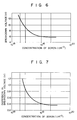
- Fig. 6 represents the relationship between the boron concentration of the P type region of the diode and the breakdown voltage of the diode.
- Fig. 7 shows the relationship between this boron concentration and the difference in breakdown voltage among the diodes.
- Fig. 8 illustrates the relationship between the boron concentration and the temperature coefficient of forward voltage.
- Fig. 9 shows the relationship between the boron concentration and the difference in temperature coefficient among the diodes.
- Polycrystalline silicon diode 35 whose P type region has a boron concentration of 1 ⁇ 1019 cm ⁇ 3, has both a design withstand voltage and a design temperature characteristic.
- the concentration of an N type impurity (e.g., phosphorus or arsenic) can be controlled for the purpose of imparting design withstand voltage and temperature characteristic to the diode.
- the concentration of the N type impurity is set to be 1 ⁇ 1019 cm ⁇ 3.
- Fig. 10 shows another control section which is formed in control region 13.
- This control section comprises unit 100 for protecting the device against an excessive temperature rise, hysteresis unit 200 and gate-protecting unit 300.
- Unit 100 is similar to the protective unit shown in Fig. 3.
- polycrystalline silicon diode 25 lateral type MOS transistor 26, polycrystalline silicon resistor 27 (271 - 275), constant-voltage zener diode 28, and like are formed on control region 13, i.e., the center portion of semiconductor substrate 11, side by side in the same plane as is illustrated in Fig. 1.
- Polycrystalline silicon diode 25, or a heat-sensitive element, is composed of a plurality of silicon islands. The silicon islands form the PN junctions of series-connected diode elements.
- Hysteresis unit 200 comprises MOS transistor 70, diode 71, etc. which are formed in control region 13.
- MOS transistor 70 is a lateral type transistor.
- Unit 300 comprises a number of diodes 73 which are formed either within or without control region 13.
- the control section of Fig. 10 is advantageous over the control section of Fig. 3 in the following respect.
- the drain of power MOS transistor 22 may oscillates when it is heated to the reference temperature or thereabout.
- hysteresis unit 200 gives hysteresis to the operating point of control MOS transistor 26, thereby preventing the drain of power MOS transistor from oscillating.
- lateral type MOS transistor 70, resistor 275 and level-shifting diode 71 cooperate to vary the potential at the point corresponding to the gate of lateral type MOS transistor 26.
- Gate voltage Vg of power MOS transistor 22 can thereby have such hysteresis as is illustrated in Fig. 11.
- MOS transistor 70 As long as the temperature of silicon substrate 111 remains below the reference value, power MOS transistor 22 is on due to input voltage Vin, and MOS transistor 70 is also on.
- the resistance which MOS transistor 70 has in this condition is negligibly small in comparison with the resistance of resistor 275.
- the resistance of resistor 275 is much higher than the resistance which MOS transistor 70 exhibits when it is turned on. Therefore, the gate voltage of MOS transistor 26 is determined by the resistance of resistor 273 and the current flowing through resistor 273.
- MOS transistor 26 When the temperature of silicon substrate 111 rises above the reference value, the forward voltage of polycrystalline silicon diode 25 (i.e., the heat-sensitive element) falls. As a result, the voltage between the ends of resistor 273 proportionately rises. When this voltage exceeds a predetermined value, MOS transistor 26 is turned on. More specifically, MOS transistor 26 is turned on when its junction temperature rises to 150°C or thereabout. Therefore, the gate voltage Vg of power MOS transistor 22 falls, and transistor 22 is turned off. Also, lateral type MOS transistor 70 is turned off. While power MOS transistor 22 is off, resistor 275 and diode 71 are connected in series to resistor 273 The resistance of this portion therefore increases.
- Fig. 12 shows still another control section according to the invention.
- This control section is, so to speak, a combination of the control section shown in Fig. 10 and unit 400 for protecting the semiconductor device against an excessively large current.
- Unit 400 has vertical type power MOS transistor 74.
- Transistor 74 is formed in the region where power MOS transistor 22 is formed. Its source electrode occupies a tiny portion of this region, i.e., 1/100 to 1/3000 of the region, and is electrically separated from transistor 22. Transistor 74 is driven by the same gate voltage as is applied to power MOS transistor 22, and outputs a small current proportional to the output current of power MOS tansistor 22.
- MOS transistor 75 is formed in the same substrate as other lateral MOS transistors 26 and 70.
- Unit 400 has a stabilization point which is determined by circuit constants, such as the area ratio of power MOS transistor 22 to MOS transistor 74, the resistance of resistor 276, the threshold voltage of MOS transistor 75, and the ratio of the on-resistance of transistor 74 to the resistance of resistor 276. Hence, a maximum current is determined in accordance with this stabilization point.
- the current ability of power MOS transistor 22 would indefinitely increases as the drain voltage increases. As long as the drain voltage is below a specific value (e.g., 2 volts), the current ability of transistor 22 increases in the same way as it would if unit 400 were not provided. However, once the drain voltage rises above this specific value, the drain current of MOS transistor 22 remains at a substantially constant value.
- a specific value e.g. 2 volts
- the load current is limited to a specific value.
- the semiconductor elements and wiring of the semiconductor device can be reliably protected from an excessively large current.
Landscapes
- Semiconductor Integrated Circuits (AREA)
- Metal-Oxide And Bipolar Metal-Oxide Semiconductor Integrated Circuits (AREA)
Claims (8)
- Dispositif semi-conducteur comprenant :[a] un substrat semi-conducteur (11) ;[b] au moins un élément semi-conducteur actif (22) étant formé sur ledit substrat semi-conducteur (11) dans une zone de puissance (12) de celui-ci ;[c] un élément sensible à la chaleur (25) pour détecter la température dudit substrat semi-conducteur (11) ; et[d] une section de commande (13) qui interrompt toute génération de chaleur supplémentaire dudit (desdits) élément(s) semi-conducteur(s) actif(s) (22) lorsque la température détectée par ledit élément sensible à la chaleur (25) dépasse une valeur prédéterminée,[e] ledit élément sensible à la chaleur (25) et ladite section de commande (13) étant formés sur ledit substrat semi-conducteur (11) dans une zone de commande (13) de celui-ci ;
caractérisé en ce que[f] ledit élément sensible à la chaleur (25) est logé dans la zone de commande (13) qui est substantiellement située dans la partie centrale dudit substrat semi-conducteur (11)[f1] et séparée de ladite zone de puissance (12) ;[g] ledit élément sensible à la chaleur (25) est formé sur un film isolant (24) qui est formé sur au moins une partie de ladite zone de commande (13) ; et[h] ladite section de commande (13) est formée dans la partie restante de ladite zone de commande (13). - Dispositif semi-conducteur selon la revendication 1, caractérisé en ce que ledit élément sensible à la chaleur consiste en un élément semi-conducteur ayant une jonction PN faite de silicium polycristallin formé sur ledit film s'isolation (24), la tension en sens direct de ladite jonction PN variant au gré des changements de température dudit substrat semi-conducteur (11).
- Dispositif semi-conducteur selon la revendication 1, caractérisé en ce que ledit élément sensible à la chaleur (25) consiste en une pluralité de diodes de silicium polycristallin connectées en séries et ayant chaucune une jonction PN qui est faite de silicium polycristallin formé sur ledit film isolant (24).
- Dispositif semi-conducteur selon la revendication 1, caractérisé en ce que ledit élément sensible à la chaleur (25) consiste une jonction PN faite de silicium polycristallin formé sur ledit film isolant (24), une zone de concentration à faible impureté dans la zone P ou N de ladite jonction PN ayant une concentration d'impureté d'au moins 1 x 10¹⁹ cm⁻³.
- Dispositif semi-conducteur selon la revendication 4, caractérisé en ce que ladite zone de concentration de faible impureté est dopée au bore.
- Dispositif semi-conducteur selon l'une des revendications 1 à 5, caractérisé en ce que ladite zone de commande (13) comporte une pluralité de résistances (217 à 272) dont au moins une est une résistance en silicium polycristallin formée sur ledit film isolant (24).
- Dispositif semi-conducteur selon l'une des revendications 1 à 6, caractérisé en ce que ledit élément semi-conducteur actif (22) formé dans ladite zone de puissance (12) est un transistor de puissance MOS du type vertical.
- Dispositif semi-conducteur selon l'une des revendications 1 à 7, caractérisé en ce que ladite section de commande (13) comporte un transistor MOS (26) du type latéral qui est formé dans la zone de surface dudit substrat semi-conducteur (11) et qui est connecté pour recevoir un signal dudit élément sensible à la chaleur (25).
Applications Claiming Priority (2)
| Application Number | Priority Date | Filing Date | Title |
|---|---|---|---|
| JP27014185 | 1985-11-29 | ||
| JP270141/85 | 1985-11-29 |
Publications (3)
| Publication Number | Publication Date |
|---|---|
| EP0224274A2 EP0224274A2 (fr) | 1987-06-03 |
| EP0224274A3 EP0224274A3 (en) | 1990-01-17 |
| EP0224274B1 true EP0224274B1 (fr) | 1993-03-10 |
Family
ID=17482115
Family Applications (1)
| Application Number | Title | Priority Date | Filing Date |
|---|---|---|---|
| EP86116560A Expired - Lifetime EP0224274B1 (fr) | 1985-11-29 | 1986-11-28 | Dispositif à semi-conducteur ayant des moyens le protégeant contre la surchauffe |
Country Status (4)
| Country | Link |
|---|---|
| US (2) | US4760434A (fr) |
| EP (1) | EP0224274B1 (fr) |
| JP (1) | JPH0693485B2 (fr) |
| DE (1) | DE3687952T2 (fr) |
Cited By (1)
| Publication number | Priority date | Publication date | Assignee | Title |
|---|---|---|---|---|
| US5994752A (en) * | 1995-09-18 | 1999-11-30 | Siemens Aktiengesellschaft | Field-effect-controllable semiconductor component with a plurality of temperature sensors |
Families Citing this family (124)
| Publication number | Priority date | Publication date | Assignee | Title |
|---|---|---|---|---|
| JP3746604B2 (ja) | 1997-12-09 | 2006-02-15 | 株式会社ルネサステクノロジ | 半導体装置およびその製造方法 |
| US5136348A (en) * | 1986-10-08 | 1992-08-04 | Nippondenso Co., Ltd. | Structure and manufacturing method for thin-film semiconductor diode device |
| US4896196A (en) * | 1986-11-12 | 1990-01-23 | Siliconix Incorporated | Vertical DMOS power transistor with an integral operating condition sensor |
| US4920388A (en) * | 1987-02-17 | 1990-04-24 | Siliconix Incorporated | Power transistor with integrated gate resistor |
| US5241210A (en) * | 1987-02-26 | 1993-08-31 | Kabushiki Kaisha Toshiba | High breakdown voltage semiconductor device |
| US4893158A (en) * | 1987-06-22 | 1990-01-09 | Nissan Motor Co., Ltd. | MOSFET device |
| JP2521783B2 (ja) * | 1987-09-28 | 1996-08-07 | 三菱電機株式会社 | 半導体装置およびその製造方法 |
| DE3844958C2 (de) * | 1987-09-28 | 1999-04-22 | Mitsubishi Electric Corp | Integrierte Halbleiteranordnung mit Überlastschutz |
| EP0322860B1 (fr) * | 1987-12-28 | 1996-09-11 | Fuji Electric Co., Ltd. | Dispositif semi-conducteur à grille isolée |
| US5049961A (en) * | 1989-01-10 | 1991-09-17 | Ixys Corporation | Monolithic temperature sensing device |
| US5119162A (en) * | 1989-02-10 | 1992-06-02 | Texas Instruments Incorporated | Integrated power DMOS circuit with protection diode |
| US5173755A (en) * | 1989-05-12 | 1992-12-22 | Western Digital Corporation | Capacitively induced electrostatic discharge protection circuit |
| US5128823A (en) * | 1989-06-14 | 1992-07-07 | Nippondenso Co., Ltd. | Power semiconductor apparatus |
| US5100829A (en) * | 1989-08-22 | 1992-03-31 | Motorola, Inc. | Process for forming a semiconductor structure with closely coupled substrate temperature sense element |
| US5025298A (en) * | 1989-08-22 | 1991-06-18 | Motorola, Inc. | Semiconductor structure with closely coupled substrate temperature sense element |
| FR2655196B1 (fr) * | 1989-11-29 | 1992-04-10 | Sgs Thomson Microelectronics | Circuit d'isolation dynamique de circuits integres. |
| JPH03238868A (ja) * | 1990-02-15 | 1991-10-24 | Nec Corp | 縦型電界効果トランジスタ |
| US5237194A (en) * | 1990-04-27 | 1993-08-17 | Nec Corporation | Power semiconductor device |
| JPH0496267A (ja) * | 1990-08-03 | 1992-03-27 | Sharp Corp | 半導体集積回路 |
| US5444219A (en) * | 1990-09-24 | 1995-08-22 | U.S. Philips Corporation | Temperature sensing device and a temperature sensing circuit using such a device |
| US5798550A (en) * | 1990-10-01 | 1998-08-25 | Nippondenso Co. Ltd. | Vertical type semiconductor device and gate structure |
| JP2751612B2 (ja) * | 1990-10-01 | 1998-05-18 | 株式会社デンソー | 縦型パワートランジスタ及びその製造方法 |
| US5079608A (en) * | 1990-11-06 | 1992-01-07 | Harris Corporation | Power MOSFET transistor circuit with active clamp |
| US5206778A (en) * | 1991-05-16 | 1993-04-27 | International Business Machines Corporation | Sense circuit for on-chip thermal shutdown |
| DE4122653C2 (de) * | 1991-07-09 | 1996-04-11 | Daimler Benz Ag | Steuerbare Halbleiterschalteinrichtung mit integrierter Strombegrenzung und Übertemperaturabschaltung |
| US5250834A (en) * | 1991-09-19 | 1993-10-05 | International Business Machines Corporation | Silicide interconnection with schottky barrier diode isolation |
| US5266831A (en) * | 1991-11-12 | 1993-11-30 | Motorola, Inc. | Edge termination structure |
| JP3337079B2 (ja) * | 1991-11-26 | 2002-10-21 | ローム株式会社 | 電源回路 |
| US5304837A (en) * | 1992-01-08 | 1994-04-19 | Siemens Aktiengesellschaft | Monolithically integrated temperature sensor for power semiconductor components |
| US5401997A (en) * | 1992-01-22 | 1995-03-28 | Integrated Device Technology, Inc. | ESD protection for poly resistor on oxide |
| JP3216206B2 (ja) * | 1992-03-30 | 2001-10-09 | 株式会社デンソー | 半導体装置及びその製造方法 |
| JP3168763B2 (ja) * | 1992-03-30 | 2001-05-21 | 株式会社デンソー | 半導体装置及びその製造方法 |
| JP3031059B2 (ja) * | 1992-05-15 | 2000-04-10 | 日産自動車株式会社 | 負荷短絡保護機能付きmos形パワー素子 |
| GB9215654D0 (en) * | 1992-07-23 | 1992-09-09 | Philips Electronics Uk Ltd | A semiconductor component |
| US5461252A (en) * | 1992-10-06 | 1995-10-24 | Matsushita Electric Industrial Co., Ltd. | Semiconductor device comprising an over-temperature detection element for detecting excessive temperature of amplifiers |
| DE4236333A1 (de) * | 1992-10-28 | 1994-05-05 | Bosch Gmbh Robert | Monolithich integriertes MOS-Endstufenbauteil mit einer Übertemperatur-Schutzeinrichtung |
| DE4236334A1 (de) * | 1992-10-28 | 1994-05-05 | Bosch Gmbh Robert | Monolithisch integriertes MOS-Endstufenbauteil mit einer Überlast-Schutzeinrichtung |
| JP2956434B2 (ja) * | 1992-10-30 | 1999-10-04 | 株式会社デンソー | 絶縁分離形半導体装置 |
| US5633526A (en) * | 1992-11-01 | 1997-05-27 | Rohm Co., Ltd. | Photodiode array and method for manufacturing the same |
| DE4305038C2 (de) * | 1993-02-18 | 1998-02-05 | Siemens Ag | MOSFET mit Temperaturschutz |
| GB9313651D0 (en) * | 1993-07-01 | 1993-08-18 | Philips Electronics Uk Ltd | A semiconductor device |
| JP3982842B2 (ja) * | 1993-08-18 | 2007-09-26 | 株式会社ルネサステクノロジ | 半導体装置 |
| JP3125529B2 (ja) * | 1993-08-23 | 2001-01-22 | 富士電機株式会社 | 半導体装置 |
| US5497285A (en) * | 1993-09-14 | 1996-03-05 | International Rectifier Corporation | Power MOSFET with overcurrent and over-temperature protection |
| US5548205A (en) * | 1993-11-24 | 1996-08-20 | National Semiconductor Corporation | Method and circuit for control of saturation current in voltage regulators |
| JPH07161920A (ja) * | 1993-12-08 | 1995-06-23 | Nec Corp | 半導体集積回路 |
| JP2630242B2 (ja) * | 1993-12-28 | 1997-07-16 | 日本電気株式会社 | 温度検出用ダイオード付パワーmosfet |
| US6092927A (en) * | 1994-11-10 | 2000-07-25 | International Rectifier Corp. | Temperature detection of power semiconductors performed by a co-packaged analog integrated circuit |
| US5639163A (en) * | 1994-11-14 | 1997-06-17 | International Business Machines Corporation | On-chip temperature sensing system |
| US5517053A (en) * | 1995-01-09 | 1996-05-14 | Northrop Grumman Corporation | Self stabilizing heater controlled oscillating transistor |
| GB9513420D0 (en) * | 1995-06-30 | 1995-09-06 | Philips Electronics Uk Ltd | Power semiconductor devices |
| DE69527146T2 (de) * | 1995-11-10 | 2002-12-12 | Co.Ri.M.Me. Consorzio Per La Ricerca Sulla Microelettronica Nel Mezzogiorno, Catania | Integriertes MOS-Bauelement mit einer Gateschutzdiode |
| JPH09213956A (ja) * | 1996-02-07 | 1997-08-15 | Nec Kansai Ltd | 半導体装置及びその製造方法 |
| US5949121A (en) * | 1996-08-02 | 1999-09-07 | Motorola Inc. | Temperature-indicating field effect transistor |
| JP3521648B2 (ja) * | 1996-09-30 | 2004-04-19 | 株式会社デンソー | 半導体装置の製造方法 |
| US5838187A (en) * | 1997-02-10 | 1998-11-17 | Lucent Technologies Inc. | Integrated circuit thermal shutdown system utilizing a thermal sensor |
| SG55452A1 (en) * | 1997-02-12 | 1998-12-21 | Int Rectifier Corp | Method and circuit to sense the tj of mos-gated power semi conductor devices |
| US5716880A (en) * | 1997-02-20 | 1998-02-10 | Chartered Semiconductor Manufacturing Pte Ltd. | Method for forming vertical polysilicon diode compatible with CMOS/BICMOS formation |
| JP3752796B2 (ja) * | 1997-03-26 | 2006-03-08 | 日産自動車株式会社 | 温度検知回路 |
| US6088208A (en) * | 1997-03-31 | 2000-07-11 | Matsushita Electronics Corporation | Electronic device, electronic switching apparatus including the same, and production method thereof |
| DE19727229C1 (de) * | 1997-06-26 | 1998-07-23 | Siemens Ag | Schaltungsanordnung zum Erfassen des Überschreitens einer kritischen Temperatur eines Bauelements |
| US6172383B1 (en) | 1997-12-31 | 2001-01-09 | Siliconix Incorporated | Power MOSFET having voltage-clamped gate |
| US6268242B1 (en) | 1997-12-31 | 2001-07-31 | Richard K. Williams | Method of forming vertical mosfet device having voltage clamped gate and self-aligned contact |
| US6015993A (en) * | 1998-08-31 | 2000-01-18 | International Business Machines Corporation | Semiconductor diode with depleted polysilicon gate structure and method |
| US6203191B1 (en) | 1998-10-28 | 2001-03-20 | Speculative Incorporated | Method of junction temperature determination and control utilizing heat flow |
| JP2000286391A (ja) * | 1999-03-31 | 2000-10-13 | Fuji Electric Co Ltd | レベルシフタ |
| JP3650281B2 (ja) * | 1999-05-07 | 2005-05-18 | セイコーインスツル株式会社 | 半導体装置 |
| US6137165A (en) * | 1999-06-25 | 2000-10-24 | International Rectifier Corp. | Hybrid package including a power MOSFET die and a control and protection circuit die with a smaller sense MOSFET |
| JP3926975B2 (ja) * | 1999-09-22 | 2007-06-06 | 株式会社東芝 | スタック型mosトランジスタ保護回路 |
| US6329690B1 (en) * | 1999-10-22 | 2001-12-11 | International Business Machines Corporation | Method and apparatus to match semiconductor device performance |
| US6642577B2 (en) * | 2000-03-16 | 2003-11-04 | Denso Corporation | Semiconductor device including power MOSFET and peripheral device and method for manufacturing the same |
| JP2002050640A (ja) * | 2000-05-22 | 2002-02-15 | Sony Corp | 電界効果トランジスタの保護回路及び半導体装置 |
| JP3482948B2 (ja) | 2000-07-25 | 2004-01-06 | 株式会社デンソー | 半導体装置 |
| JP2002208702A (ja) * | 2001-01-10 | 2002-07-26 | Mitsubishi Electric Corp | パワー半導体装置 |
| JP4620889B2 (ja) * | 2001-03-22 | 2011-01-26 | 三菱電機株式会社 | 電力用半導体装置 |
| JP2002313924A (ja) * | 2001-04-09 | 2002-10-25 | Seiko Instruments Inc | 半導体装置 |
| US6633063B2 (en) * | 2001-05-04 | 2003-10-14 | Semiconductor Components Industries Llc | Low voltage transient voltage suppressor and method of making |
| US6906399B2 (en) * | 2002-11-04 | 2005-06-14 | Delphi Technologies, Inc. | Integrated circuit including semiconductor power device and electrically isolated thermal sensor |
| EP1424766A1 (fr) * | 2002-11-29 | 2004-06-02 | STMicroelectronics S.r.l. | Régulateur de tension à découpage |
| US20040150417A1 (en) * | 2003-01-30 | 2004-08-05 | Paulos John James | Integrated circuit with junction temperature sensing diode |
| US6841437B1 (en) * | 2003-06-20 | 2005-01-11 | Semiconductor Components Industries, L.L.C. | Method of forming a vertical power semiconductor device and structure therefor |
| KR100687018B1 (ko) * | 2003-09-26 | 2007-02-27 | 마츠시타 덴끼 산교 가부시키가이샤 | 과열보호회로를 구비한 반도체장치 및 그것을 이용한전자회로 |
| JP2005167075A (ja) * | 2003-12-04 | 2005-06-23 | Denso Corp | 半導体装置 |
| JP4765252B2 (ja) * | 2004-01-13 | 2011-09-07 | 株式会社豊田自動織機 | 温度検出機能付き半導体装置 |
| DE102005016830A1 (de) * | 2004-04-14 | 2005-11-03 | Denso Corp., Kariya | Halbleitervorrichtung und Verfahren zu ihrer Herstellung |
| US7406397B2 (en) * | 2004-09-02 | 2008-07-29 | International Business Machines Corporation | Self heating monitor for SiGe and SOI CMOS devices |
| JP4641164B2 (ja) * | 2004-09-14 | 2011-03-02 | ルネサスエレクトロニクス株式会社 | 過熱検出回路 |
| US20060066335A1 (en) * | 2004-09-28 | 2006-03-30 | Kang Seung H | Semiconductor test device with heating circuit |
| WO2006068082A1 (fr) * | 2004-12-22 | 2006-06-29 | Mitsubishi Denki Kabushiki Kaisha | Dispositif a semiconducteur |
| WO2007006337A1 (fr) * | 2005-07-13 | 2007-01-18 | Freescale Semiconductor, Inc. | Sonde de temperature |
| JP2007049012A (ja) * | 2005-08-11 | 2007-02-22 | Nec Electronics Corp | 半導体装置 |
| CN100449901C (zh) * | 2005-09-22 | 2009-01-07 | 华为技术有限公司 | 一种防止设备内部燃烧向外蔓延的装置 |
| DE102006013721B4 (de) * | 2006-03-24 | 2011-12-08 | Infineon Technologies Ag | Halbleiterschaltungsanordnung und zugehöriges Verfahren zur Temperaturerfassung |
| JP5098214B2 (ja) | 2006-04-28 | 2012-12-12 | 日産自動車株式会社 | 半導体装置およびその製造方法 |
| US20080026181A1 (en) * | 2006-07-25 | 2008-01-31 | Ravi Rastogi | Synergistically-modified surfaces and surface profiles for use with thermal interconnect and interface materials, methods of production and uses thereof |
| US8476709B2 (en) | 2006-08-24 | 2013-07-02 | Infineon Technologies Ag | ESD protection device and method |
| JP2008244487A (ja) * | 2008-04-21 | 2008-10-09 | Renesas Technology Corp | 複合型mosfet |
| CN101901180B (zh) * | 2009-05-25 | 2013-01-23 | 和硕联合科技股份有限公司 | 加热保护电路、电子装置及其加热保护方法 |
| JP5333342B2 (ja) | 2009-06-29 | 2013-11-06 | 株式会社デンソー | 半導体装置 |
| ITMI20121599A1 (it) | 2012-09-25 | 2014-03-26 | St Microelectronics Srl | Dispositivo elettronico comprendente un transistore vtmos ed un diodo termico integrati |
| US9966584B2 (en) | 2013-03-11 | 2018-05-08 | Atieva, Inc. | Bus bar for battery packs |
| US10084214B2 (en) | 2013-03-15 | 2018-09-25 | Atieva, Inc. | Automatic switchover from cell voltage to interconnect voltage monitoring |
| US9041454B2 (en) * | 2013-03-15 | 2015-05-26 | Atieva, Inc. | Bias circuit for a switched capacitor level shifter |
| US10063071B2 (en) | 2013-03-15 | 2018-08-28 | Atieva, Inc. | Balance resistor and low pass filter |
| US10901019B2 (en) | 2013-03-15 | 2021-01-26 | Atieva, Inc. | Method of connecting cell voltage sensors |
| JP6107937B2 (ja) | 2013-04-05 | 2017-04-05 | 富士電機株式会社 | 半導体装置の駆動方法 |
| US9048838B2 (en) | 2013-10-30 | 2015-06-02 | Infineon Technologies Austria Ag | Switching circuit |
| US9525063B2 (en) | 2013-10-30 | 2016-12-20 | Infineon Technologies Austria Ag | Switching circuit |
| US20150116882A1 (en) * | 2013-10-31 | 2015-04-30 | Analog Devices, Inc. | Apparatus and method for time-delayed thermal overload protection |
| JP6345930B2 (ja) * | 2013-12-26 | 2018-06-20 | ローム株式会社 | 半導体装置およびその設計方法 |
| DE102014109147A1 (de) * | 2014-06-30 | 2015-12-31 | Infineon Technologies Ag | Feldeffekthalbleiter-Bauelement sowie Verfahren zu dessen Betrieb und Herstellung |
| US9768766B2 (en) | 2014-07-14 | 2017-09-19 | Infineon Technologies Austria Ag | Electronic switching element and integrated sensor |
| JP6436791B2 (ja) * | 2015-01-16 | 2018-12-12 | エイブリック株式会社 | 半導体装置 |
| US9917578B2 (en) | 2016-02-19 | 2018-03-13 | Infineon Technologies Austria Ag | Active gate-source capacitance clamp for normally-off HEMT |
| US10411006B2 (en) * | 2016-05-09 | 2019-09-10 | Infineon Technologies Ag | Poly silicon based interface protection |
| JP6414159B2 (ja) * | 2016-07-29 | 2018-10-31 | トヨタ自動車株式会社 | 半導体装置およびその製造方法 |
| TWI655748B (zh) * | 2016-12-16 | 2019-04-01 | 通嘉科技股份有限公司 | 具有熱敏單元的垂直雙擴散金氧半功率元件 |
| JP6922563B2 (ja) * | 2017-08-31 | 2021-08-18 | 富士電機株式会社 | 半導体装置 |
| CN108109999A (zh) * | 2018-01-16 | 2018-06-01 | 上海南麟电子股份有限公司 | 过温保护电路、半导体器件及其制备方法 |
| JP7135445B2 (ja) * | 2018-05-29 | 2022-09-13 | 富士電機株式会社 | 半導体装置 |
| US11579645B2 (en) * | 2019-06-21 | 2023-02-14 | Wolfspeed, Inc. | Device design for short-circuitry protection circuitry within transistors |
| US11621206B2 (en) | 2020-08-05 | 2023-04-04 | Nxp Usa, Inc. | Amplifier with integrated temperature sensor |
| US12313476B2 (en) * | 2021-07-01 | 2025-05-27 | Microchip Technology Incorporated | Temperature sensor integrated in a transistor array |
| JP7732280B2 (ja) * | 2021-08-27 | 2025-09-02 | 富士電機株式会社 | 半導体モジュール |
Family Cites Families (20)
| Publication number | Priority date | Publication date | Assignee | Title |
|---|---|---|---|---|
| JPS5272183A (en) * | 1975-12-12 | 1977-06-16 | Mitsubishi Electric Corp | Semiconductor device with protecting device |
| JPS5359385A (en) * | 1976-11-09 | 1978-05-29 | Mitsubishi Electric Corp | Production method of semiconductor thermal sensitive element |
| US4229753A (en) * | 1977-08-18 | 1980-10-21 | International Business Machines Corporation | Voltage compensation of temperature coefficient of resistance in an integrated circuit resistor |
| US4198581A (en) * | 1977-10-13 | 1980-04-15 | Rca Corporation | Temperature compensating comparator |
| IT1202895B (it) * | 1979-02-27 | 1989-02-15 | Ates Componenti Elettron | Dispositivo di protezione termica per un componente elettronico a semiconduttore |
| JPS55140261A (en) * | 1979-04-19 | 1980-11-01 | Chiyou Lsi Gijutsu Kenkyu Kumiai | Substrate potential generator |
| JPS5635383A (en) * | 1979-08-29 | 1981-04-08 | Kyoto Ceramic | Semiconductor integrated circuit support with heating mechanism |
| JPS5913445B2 (ja) * | 1980-02-22 | 1984-03-29 | 工業技術院長 | ホウ酸カルシウムの製造方法 |
| JPS56120153A (en) * | 1980-02-28 | 1981-09-21 | Seiko Epson Corp | Temperature protector for integrated circuit |
| JPS57113332A (en) * | 1980-12-30 | 1982-07-14 | Horiba Ltd | Compensating thermopile detector |
| JPS57141962A (en) * | 1981-02-27 | 1982-09-02 | Hitachi Ltd | Semiconductor integrated circuit device |
| JPS57145355A (en) * | 1981-03-04 | 1982-09-08 | Nippon Denso Co Ltd | Semiconductor device |
| DE3138535A1 (de) * | 1981-09-28 | 1983-04-07 | Siemens AG, 1000 Berlin und 8000 München | Temperatursensor mit einem halbleiterkoerper |
| JPS5884461A (ja) * | 1981-11-13 | 1983-05-20 | Hitachi Ltd | 絶縁ゲ−ト型半導体装置 |
| JPS58138074A (ja) * | 1982-02-12 | 1983-08-16 | Toshiba Corp | 入力保護回路 |
| JPS59163528A (ja) * | 1983-03-09 | 1984-09-14 | Seiko Epson Corp | 温度検出回路 |
| JPS59224172A (ja) * | 1983-06-03 | 1984-12-17 | Hitachi Ltd | 半導体回路装置における破壊防止回路 |
| JPS6072254A (ja) * | 1983-09-28 | 1985-04-24 | Matsushita Electric Ind Co Ltd | 半導体装置 |
| DE3532228A1 (de) * | 1984-10-02 | 1986-04-17 | Toshiba Ceramics Co., Ltd., Tokio/Tokyo | Feuerfeste zusammensetzung |
| JPH05272183A (ja) * | 1992-03-24 | 1993-10-19 | Naka Ind Ltd | パネル壁面の構造 |
-
1986
- 1986-10-21 JP JP61250208A patent/JPH0693485B2/ja not_active Expired - Lifetime
- 1986-11-28 EP EP86116560A patent/EP0224274B1/fr not_active Expired - Lifetime
- 1986-11-28 US US06/935,718 patent/US4760434A/en not_active Expired - Lifetime
- 1986-11-28 DE DE86116560T patent/DE3687952T2/de not_active Expired - Lifetime
-
1988
- 1988-03-16 US US07/169,001 patent/US4896199A/en not_active Expired - Lifetime
Cited By (1)
| Publication number | Priority date | Publication date | Assignee | Title |
|---|---|---|---|---|
| US5994752A (en) * | 1995-09-18 | 1999-11-30 | Siemens Aktiengesellschaft | Field-effect-controllable semiconductor component with a plurality of temperature sensors |
Also Published As
| Publication number | Publication date |
|---|---|
| DE3687952D1 (de) | 1993-04-15 |
| EP0224274A2 (fr) | 1987-06-03 |
| US4896199A (en) | 1990-01-23 |
| DE3687952T2 (de) | 1993-09-30 |
| US4760434A (en) | 1988-07-26 |
| JPH0693485B2 (ja) | 1994-11-16 |
| EP0224274A3 (en) | 1990-01-17 |
| JPS62229866A (ja) | 1987-10-08 |
Similar Documents
| Publication | Publication Date | Title |
|---|---|---|
| EP0224274B1 (fr) | Dispositif à semi-conducteur ayant des moyens le protégeant contre la surchauffe | |
| US4893158A (en) | MOSFET device | |
| JP3911566B2 (ja) | Mos型半導体装置 | |
| US5642252A (en) | Insulated gate semiconductor device and driving circuit device and electronic system both using the same | |
| US5162966A (en) | Semiconductor device having a surge protecting element | |
| JP2731119B2 (ja) | 半導体パワー素子およびその遮断回路 | |
| US5237194A (en) | Power semiconductor device | |
| US5629542A (en) | Compounded power MOSFET | |
| EP0485174B1 (fr) | Circuit à transistor de puissance MOSFET avec un verrouillage actif | |
| US4994904A (en) | MOSFET having drain voltage detection function | |
| US6323518B1 (en) | Insulated gate type semiconductor device and method of manufacturing thereof | |
| US20050286194A1 (en) | Power transistor device and a power control system for using it | |
| EP0292782B1 (fr) | Mosfet vertical comprenant une diode de régulation de tension située à une faible profondeur par rapport à la surface | |
| JPH0433139B2 (fr) | ||
| JPH11266016A (ja) | 半導体装置およびその製造方法 | |
| EP0733283A1 (fr) | Commutateur protege | |
| JPH081956B2 (ja) | 保護機能を備えた縦型mosfet | |
| JP2522208B2 (ja) | 半導体装置 | |
| JP2680788B2 (ja) | 集積化構造の能動クランプ装置 | |
| US5491357A (en) | Integrated structure current sensing resistor for power MOS devices, particularly for overload self-protected power MOS devices | |
| EP0869342B1 (fr) | Dispositif électronique de mesure de température, et appareil de commutation électronique le contenant | |
| JPH0795657B2 (ja) | 保護機能内蔵型mosfet | |
| KR100200538B1 (ko) | 부성 저항 특성을 갖는 보호소자를 구비한 반도체장치 | |
| EP0580242B1 (fr) | Composant semiconducteur comprenant des moyens de protection | |
| EP0341730B1 (fr) | Dispositif de commande semi-conducteur bidirectionnel commandé par une grille |
Legal Events
| Date | Code | Title | Description |
|---|---|---|---|
| PUAI | Public reference made under article 153(3) epc to a published international application that has entered the european phase |
Free format text: ORIGINAL CODE: 0009012 |
|
| AK | Designated contracting states |
Kind code of ref document: A2 Designated state(s): DE FR GB IT |
|
| PUAL | Search report despatched |
Free format text: ORIGINAL CODE: 0009013 |
|
| AK | Designated contracting states |
Kind code of ref document: A3 Designated state(s): DE FR GB IT |
|
| RHK1 | Main classification (correction) |
Ipc: H01L 27/02 |
|
| 17P | Request for examination filed |
Effective date: 19900503 |
|
| 17Q | First examination report despatched |
Effective date: 19910508 |
|
| GRAA | (expected) grant |
Free format text: ORIGINAL CODE: 0009210 |
|
| AK | Designated contracting states |
Kind code of ref document: B1 Designated state(s): DE FR GB IT |
|
| REF | Corresponds to: |
Ref document number: 3687952 Country of ref document: DE Date of ref document: 19930415 |
|
| ET | Fr: translation filed | ||
| ITF | It: translation for a ep patent filed | ||
| PLBE | No opposition filed within time limit |
Free format text: ORIGINAL CODE: 0009261 |
|
| STAA | Information on the status of an ep patent application or granted ep patent |
Free format text: STATUS: NO OPPOSITION FILED WITHIN TIME LIMIT |
|
| 26N | No opposition filed | ||
| REG | Reference to a national code |
Ref country code: GB Ref legal event code: IF02 |
|
| PGFP | Annual fee paid to national office [announced via postgrant information from national office to epo] |
Ref country code: FR Payment date: 20051108 Year of fee payment: 20 |
|
| PGFP | Annual fee paid to national office [announced via postgrant information from national office to epo] |
Ref country code: GB Payment date: 20051123 Year of fee payment: 20 |
|
| PGFP | Annual fee paid to national office [announced via postgrant information from national office to epo] |
Ref country code: DE Payment date: 20051124 Year of fee payment: 20 |
|
| PGFP | Annual fee paid to national office [announced via postgrant information from national office to epo] |
Ref country code: IT Payment date: 20051128 Year of fee payment: 20 |
|
| REG | Reference to a national code |
Ref country code: GB Ref legal event code: PE20 |
|
| PG25 | Lapsed in a contracting state [announced via postgrant information from national office to epo] |
Ref country code: GB Free format text: LAPSE BECAUSE OF EXPIRATION OF PROTECTION Effective date: 20061127 |