EP0225969B1 - Apparat und Methode zur Regelung der Bestrahlung mittels Elektronenstrahles an bestimmten Positionen in einem Elektronenstrahltestsystem - Google Patents
Apparat und Methode zur Regelung der Bestrahlung mittels Elektronenstrahles an bestimmten Positionen in einem Elektronenstrahltestsystem Download PDFInfo
- Publication number
- EP0225969B1 EP0225969B1 EP86111289A EP86111289A EP0225969B1 EP 0225969 B1 EP0225969 B1 EP 0225969B1 EP 86111289 A EP86111289 A EP 86111289A EP 86111289 A EP86111289 A EP 86111289A EP 0225969 B1 EP0225969 B1 EP 0225969B1
- Authority
- EP
- European Patent Office
- Prior art keywords
- electron beam
- pattern data
- sample
- measured
- current
- Prior art date
- Legal status (The legal status is an assumption and is not a legal conclusion. Google has not performed a legal analysis and makes no representation as to the accuracy of the status listed.)
- Expired
Links
Images


Classifications
-
- G—PHYSICS
- G01—MEASURING; TESTING
- G01R—MEASURING ELECTRIC VARIABLES; MEASURING MAGNETIC VARIABLES
- G01R31/00—Arrangements for testing electric properties; Arrangements for locating electric faults; Arrangements for electrical testing characterised by what is being tested not provided for elsewhere
- G01R31/28—Testing of electronic circuits, e.g. by signal tracer
- G01R31/302—Contactless testing
- G01R31/305—Contactless testing using electron beams
Definitions
- the present invention relates to apparatus and method for controlling the irradiation of an electron beam at a fixed position in an electron beam tester system in which an electron beam is irradiated onto the surface of a sample to be measured such as, e.g., a large scale integrated circuit (LSI) and thereby measuring the state (potential) of the surface and, more particularly, to apparatus and method for correcting the deviation of the irradiating position due to the drift of the electron beam which is caused during measurement.
- LSI large scale integrated circuit
- an electron beam is irradiated onto the surface of a sample to be measured and the resultant secondary electron or reflected electron which will be obtained in accordance with the state (material, potential, and the like) of the surface of the sample is detected, thereby displaying the state of the surface of the sample (in the case where the sample is an LSI, circuit pattern, potential distribution, and the like) on an image display device and observing it.
- SEM scanning electron microscope apparatus
- stroboscopic scanning electron microscope apparatus or the like
- the specific pattern is searched from among the patterns of the LSI and the electron beam is irradiated to the central position of this pattern. Due to this, the risk such that the irradiating position of the electron beam is deviated from the specific pattern due to the drift of the electron beam during measurement of the sample to be measured is reduced as small as possible.
- the irradiating position of the electron beam is reset and the measurement is again performed.
- the drift of the electron beam is mainly caused due to the following factors (1) to (4).
- the dimension of the pattern onto which the electron beam will be irradiated is sufficiently large (e.g., 4 to 6 pm)
- the electron beam will hardly deviate from the pattern, so that no problem will occur.
- the pattern dimension is 2 11m or less
- the possibility will increase that the irradiating position will be deviated from the pattern due to a drift of the electron beam during the measurement so much that the measurement cannot be performed. Therefore, the reliability of the electron beam tester system deteriorates.
- the necessity of remeasurement causes a reduction in the usability of the expensive electron beam tester system and a decrease in the measurement efficiency.
- the original (measured) specific pattern needs to be determined once more. If this pattern is characteristic, it can be relatively easily searched by observing the patterns which are displayed on the image display device. However, in the case of a pattern image which is not characteristic (e.g., fine repetitive pattern), it is difficult to search for it. This also causes the reduction of the use efficiency of the electron beam tester system.
- the electron beam can be corrected during the measurement so that the electron beam can accurately irradiate the specific pattern, so that the reliability and efficiency in measurement can be improved.
- FIG. 1A shows an electron beam tester system according to an embodiment of the present invention.
- An electron beam EB emitted from an electron gun 11 is irradiated onto the surface of a sample (e.g. LSI) 14 to be measured through a blanking electrode 12 and a deflecting coil 13.
- Blanking electrode 12 controls blanking of electron beam EB generated from electron gun 11, thereby producing a pulse-form electron beam.
- Deflecting coil 13 deflects electron beam EB generated from electron gun 11, thereby allowing electron beam EB to scan on sample 14to be measured.
- Sample 14 is put on an XY stage 15. By moving XY stage 15 in the X and Y directions, the irradiating position of electron beam EB can be controlled.
- a test vector signal and an operating power source voltage are supplied from a test vector generator 16 to sample 14, so that this sample is made operative.
- the secondary electron generated from the surface of sample 14 (or, reflected electron which was reflected by the surface of sample 14) is detected by a scintillator 17.
- Electron gun 11, blanking electrode 12, deflecting coil 13, sample 14 to be measured, XY stage 15, and scintillator 17 are respectively arranged in an electron-optical-column 18.
- the current of the secondary electron detected by scintillator 17 is amplified by a preamplifier 19.
- An output current of preamplifier 19 is supplied to a current/voltage converter 20.
- Converter 20 converts the output current which is output from preamplifier 19 to the voltage corresponding to this current.
- Converter 20 has a gain control terminal 20A and a converting sensitivity of converter 20 is controlled by a gain control signal GC which is output from a CPU 21.
- the output voltage of converter 20 is supplied to an image display device 22 for displaying an image and to one input terminal of a voltage comparator 23, respectively.
- a slice level SL is supplied from CPU 21 to the other input terminal of voltage comparator 23.
- Comparator 23 functions as a binarizing circuit to binarize the output of converter 20 using a potential of slice level signal SL as a reference.
- the binarized output of comparator 23 is supplied to a shift register 24 of the serial input type.
- Shift register 24 temporarily stores the binarized data which is output from comparator 23. Shift register 24 sequentially shifts the binarized data supplied from voltage comparator 23 on the basis of a timing pulse signal TP, which is generated from a timing synchronous circuit 25. Synchronous circuit 25 generates timing pulse signals TP, and TP 2 under control of CPU 21. An output of shift register 24 is supplied to a serial/parallel converter 26. Converter 26 converts a serial signal which is output from shift register 24 into a parallel signal and supplies to CPU 21. The parallel data supplied from converter 26 to CPU 21 is then transmitted and stored into a magnetic disk device 27 serving as an external memory device. The storing operation in this case is controlled by CPU 21 (for example, by setting an address).
- Timing pulse signal TP 2 An output (timing pulse signal TP 2 ) of timing synchronous circuit 25 and data DV at a deflecting voltage level which is output from CPU 21 are supplied to a deflecting amplifier 28.
- Deflecting amplifier 28 supplies a deflection current to deflecting coil 13.
- the current flowing through deflecting coil 13 is supplied to an analog/digital converter 29 and sampled for every predetermined time interval.
- the current converted to the digital data by converter 29 is stored into magnetic disk device 27 through CPU 21.
- the digital signal as drift correction data which is generated from CPU 21 is delivered to a digital/analog converter 30.
- the drift correction data converted to the analog data by converter 30 is supplied to deflecting coil 13.
- electron gun 11, blanking electrode 12, XY stage 15, and test vector generator 16 are also controlled by CPU 21, respectively.
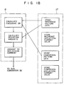
- CPU 21 and magnetic disk device 27 have the functions as shown in Figure 1B, respectively.
- Figure 2 is a flowchart showing the method of controlling the irradiation of an electron beam at a fixed position.
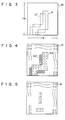
- Figure 3 is a diagram showing a pattern detection image which is obtained from image display device 22 by use of the apparatus of Figure 1.
- Figure 4 is a diagram showing a binarized data pattern which is obtained by binarizing the pattern detection image of Figure 3 by voltage comparator 23.
- Figure 5 is a diagram showing a pattern detection data which is derived by use of the apparatus of Figure 1.
- electron beam EB Prior to starting the measurement, electron beam EB is first emitted from electron gun 11 and data DV of a deflecting voltage level is given to deflecting amplifier 28, thereby deflecting electron beam EB.
- the surface of sample 14 is scanned by electron beam EB.
- the secondary electrons generated from the surface of sample 14 due to the irradiation of electron beam EB are detected by scintillator 17.
- An output current of scintillator 17 is supplied to preamplifier 19 and amplified.
- An output current of preamplifier 19 is converted to the voltage corresponding to the current by current/voltage converter 20 and this voltage signal is supplied to image display device 22.
- the image of the area scanned by the electron beam is displayed on display device 22.
- the operator changes data DV of the deflecting voltage level which is supplied to deflecting amplifier 28 or drives XY stage while observing the image on display device 22, thereby selecting one of the arbitrary pattern images displayed on display device 22 as a reference pattern image (step 1).
- a scanning area 32 of sample 14 to be measured including a selected reference pattern image 31 is scanned by electron beam EB.
- An analog current of deflecting coil 13 which is output from deflecting amplifier 28 when reference pattern image 31 is scanned by electron beam EB is converted to a digital data by analog/digital converter 29 and this digital data is stored as scanning area data into magnetic disk device 27 through CPU 21 (step 2).
- a signal (image signal) which is derived through scintillator 17, preamplifier 19, and converter 20 upon scanning of scanning area 32 is supplied to voltage comparator 23.
- Slice level signal SL serving as a reference is given from CPU 21 to comparator 23 in order to obtain the binarized reference pattern data.
- the image signal of scanning area 32 is binarized by comparator 23, so that reference pattern data as shown in Figure 4 is obtained (step 3).
- This binarized reference pattern data is supplied to shift register 24.
- the reference pattern data supplied to shift register 24 is sequentially shifted on the basis of timing pulse signal TP, which is generated from timing synchronous circuit 25 and supplied to serial/parallel converter 26.
- This serial reference pattern data supplied to converter 26 is converted to the parallel signal and input to CPU 21.
- the parallel binarized reference pattern data taken in CPU 21 is stored into magnetic disk device 27 (step 4). The initialization is completed in steps 1 to 4.
- the potentials of the various portions of a reference pattern image 31 are measured. More specifically, first, the deflection current is adjusted, thereby applying electron beam EB to a prescribed node on reference pattern image 31.
- the pulse-like electron beam derived by blanking-controlling electron beam EB by blanking electrode 12 at a predetermined timing under control of CPU 21 is irradiated onto sample 14 and a change in voltage on the prescribed node on reference pattern image 31 is measured.
- the sample (LSI) to be measured is made operative by applying a test vector signal and an operating power source voltage from test vector generator 16.
- interruption of the timer is executed by CPU 21 during the measurement so as to correct the drift of electron beam EB (step 6), thereby allowing the processes, which will be explained hereinafter, to be executed at a predetermined time interval.
- the irradiation of electron beam EB to the prescribed node on reference pattern image 31 is interrupted and data DV of the deflecting voltage level is taken out of magnetic disk device 27 to CPU 21 and supplied from CPU 21 to deflecting amplifier 28 so that electron beam EB can be irradiated onto the reference pattern image 31 which has previously stored into magnetic disk device 27 before the measurement.
- the deflection current which is output from deflecting amplifier 28 is supplied to deflecting coil 13 (step 7).
- scanning area 32 of sample 14 shown in Figure 3 is again scanned by electron beam EB.
- the output of current/voltage converter 20 which is derived through scintillator 17 and preamplifier 19 upon scanning of the electron beam is binarized by voltage comparator 23.
- This binarized signal is input to CPU 21 through shift register 24 and serial/parallel converter 26 (step 8).
- deflecting amplifier 28 and shift register 24 are synchronized by timing synchronous circuit 25. Due to this, the deflection start position can accurately correspond to the start bit of the binarized data.
- scanning widths (indicated at XW and YW in Figure 3) of electron beam EB are set to 25.6 um and the capacity of shift register 24 is 256 bits, for example, the resolution per bit of the binarized data will become 0.1 pm.
- These scanning widths XW and YW of electron beam EB may be set to a proper value in accordance with the width of pattern to be measured.
- the binarized data of the scanning area obtained during the measurement as described above and the binarized data of scanning area 32 which has previously stored into magnetic disk device 27 before the measurement are compared and processed by CPU 21 (step 9).
- This comparing process may be executed by calculating the exclusive OR of both data by CPU 21, for example.
- a broken line 31' in Figure 3 in the case where the pattern image derived during the measurement is deviated from the reference pattern image (indicated by a solid line 31) which has previously stored, the pattern of the binarized data is deviated as indicated by a broken line 31A' as compared with the pattern of the data stored in magnetic disk device 27 indicated by solid line 31A in Figure 4.
- step 10 the result of the comparison of the binarized data having such a pattern as shown in Figure 5 corresponding to an amount of deviation of the patterns between both data is obtained (step 10).
- the resolution per bit of the data of the result of the comparison has previously been known from the relation between the scanning widths XW and YW of electron beam EB and the number of bits of shift register 24 as mentioned before and corresponds to the amounts of drifts in the X and Y directions of electron beam EB on sample 14 which were caused during the measurement. Therefore, the drift amounts of electron beam EB can be calculated from the deviation amounts of those two patterns.
- DC offset bias amounts are calculated by CPU 21 in consideration of the deflecting sensitivity of deflecting coil 13 (step 11).
- the DC offset bias amounts can be calculated in the following manner. Namely, assuming that the deviation amounts of two patterns are x(dot) and y(dot), the drift amounts AXW and AYW of the electron beam respectively become
- DC offset bias amount data AX and AY are supplied to digital/analog converter 30 and these digital data are converted into the analog data.
- Analog DC offset bias amount data AX and AY which are output from converter 30 are supplied to deflecting coil 13, thereby correcting the deflection outputs in the X and Y directions (step 12). Due to this, the irradiating position of electron beam EB onto sample 14 is corrected. When the measurement is restarted (step 13), electron beam EB can be accurately irradiated at the position of specific pattern image 31 before the drift.
- the electron beam can be corrected during the measurement so that the electron beam can be accurately irradiated onto the specific pattern image. Therefore, the reliability and efficiency in measurement can 6e improved.
- Figure 6 shows an apparatus for controlling the irradiation of an electron beam at a fixed position according to another embodiment of the invention.
- a memory 33 is provided in place of shift register 24 serving as temporary storing means in Figure 1.
- the address in memory 33 is sequentially counted up by timing pulse signal TP1 which is output from timing synchronous circuit 25.
Landscapes
- Engineering & Computer Science (AREA)
- General Engineering & Computer Science (AREA)
- Physics & Mathematics (AREA)
- General Physics & Mathematics (AREA)
- Tests Of Electronic Circuits (AREA)
- Length-Measuring Devices Using Wave Or Particle Radiation (AREA)
- Electron Beam Exposure (AREA)
- Testing Of Individual Semiconductor Devices (AREA)
- Electron Sources, Ion Sources (AREA)
- Testing Or Measuring Of Semiconductors Or The Like (AREA)
Claims (8)
Applications Claiming Priority (2)
| Application Number | Priority Date | Filing Date | Title |
|---|---|---|---|
| JP181381/85 | 1985-08-19 | ||
| JP60181381A JPH0646550B2 (ja) | 1985-08-19 | 1985-08-19 | 電子ビ−ム定位置照射制御方法および電子ビ−ム定位置照射制御装置 |
Publications (2)
| Publication Number | Publication Date |
|---|---|
| EP0225969A1 EP0225969A1 (de) | 1987-06-24 |
| EP0225969B1 true EP0225969B1 (de) | 1990-03-28 |
Family
ID=16099733
Family Applications (1)
| Application Number | Title | Priority Date | Filing Date |
|---|---|---|---|
| EP86111289A Expired EP0225969B1 (de) | 1985-08-19 | 1986-08-14 | Apparat und Methode zur Regelung der Bestrahlung mittels Elektronenstrahles an bestimmten Positionen in einem Elektronenstrahltestsystem |
Country Status (4)
| Country | Link |
|---|---|
| US (1) | US4807159A (de) |
| EP (1) | EP0225969B1 (de) |
| JP (1) | JPH0646550B2 (de) |
| DE (1) | DE3669927D1 (de) |
Cited By (6)
| Publication number | Priority date | Publication date | Assignee | Title |
|---|---|---|---|---|
| US7786452B2 (en) | 2003-10-16 | 2010-08-31 | Alis Corporation | Ion sources, systems and methods |
| US7786451B2 (en) | 2003-10-16 | 2010-08-31 | Alis Corporation | Ion sources, systems and methods |
| US7804068B2 (en) | 2006-11-15 | 2010-09-28 | Alis Corporation | Determining dopant information |
| US8110814B2 (en) | 2003-10-16 | 2012-02-07 | Alis Corporation | Ion sources, systems and methods |
| US9159527B2 (en) | 2003-10-16 | 2015-10-13 | Carl Zeiss Microscopy, Llc | Systems and methods for a gas field ionization source |
| US20180033591A1 (en) * | 2016-07-27 | 2018-02-01 | Battelle Memorial Institute | Sensing analytical instrument parameters, specimen characteristics, or both from sparse datasets |
Families Citing this family (52)
| Publication number | Priority date | Publication date | Assignee | Title |
|---|---|---|---|---|
| JPS58134636U (ja) * | 1982-03-08 | 1983-09-10 | いすゞ自動車株式会社 | シリンダヘツド |
| JPH0622195B2 (ja) * | 1987-02-26 | 1994-03-23 | 東芝機械株式会社 | 荷電ビ−ム描画装置 |
| JPH065691B2 (ja) * | 1987-09-26 | 1994-01-19 | 株式会社東芝 | 半導体素子の試験方法および試験装置 |
| US5561696A (en) * | 1987-10-30 | 1996-10-01 | Hewlett-Packard Company | Method and apparatus for inspecting electrical connections |
| US5621811A (en) * | 1987-10-30 | 1997-04-15 | Hewlett-Packard Co. | Learning method and apparatus for detecting and controlling solder defects |
| US5070824A (en) * | 1988-05-30 | 1991-12-10 | Yamaha Hatsudoki Kabushiki Kaisha | Combustion chamber and valve operating mechanism for multi-valve engine |
| EP0392035B1 (de) * | 1989-04-11 | 1994-06-22 | ICT Integrated Circuit Testing Gesellschaft für HalbleiterprÀ¼ftechnik mbH | Verfahren zur Aufzeichnung oder Abbildung zeitabhängiger Potentiale in Bauelementen der Mikroelektronik |
| JP2786699B2 (ja) * | 1989-11-29 | 1998-08-13 | ヤマハ発動機株式会社 | Sohcエンジンの動弁装置 |
| US5172331A (en) * | 1989-12-18 | 1992-12-15 | Fujitsu Limited | Apparatus and method for effecting exposure of sample to charged particle beam |
| DE3941889A1 (de) * | 1989-12-19 | 1991-06-20 | Integrated Circuit Testing | Verfahren und vorrichtung zur potentialmessung auf leiterbahnen einer programmgesteuerten integrierten schaltung |
| US5259012A (en) * | 1990-08-30 | 1993-11-02 | Four Pi Systems Corporation | Laminography system and method with electromagnetically directed multipath radiation source |
| US5199054A (en) * | 1990-08-30 | 1993-03-30 | Four Pi Systems Corporation | Method and apparatus for high resolution inspection of electronic items |
| US5210487A (en) * | 1991-06-04 | 1993-05-11 | Schlumberger Technologies Inc. | Double-gated integrating scheme for electron beam tester |
| DE4433733A1 (de) * | 1993-09-21 | 1995-03-23 | Advantest Corp | IC-Analysesystem mit einer Ladungsteilchenstrahlvorrichtung |
| JPH07226426A (ja) * | 1994-02-10 | 1995-08-22 | Toshiba Corp | 電子ビ−ムテスタ及び電子ビ−ムテスタを使用したテスト方法 |
| US5687209A (en) * | 1995-04-11 | 1997-11-11 | Hewlett-Packard Co. | Automatic warp compensation for laminographic circuit board inspection |
| US5583904A (en) * | 1995-04-11 | 1996-12-10 | Hewlett-Packard Co. | Continuous linear scan laminography system and method |
| JPH09306414A (ja) * | 1996-05-15 | 1997-11-28 | Advantest Corp | 走査型電子顕微鏡を備えた電子ビーム露光装置 |
| US5945833A (en) * | 1996-11-27 | 1999-08-31 | University Of Massachusetts | Method for testing semiconductor devices which measures internal potential distribution, internal electric field, and internal doping profile |
| US6198299B1 (en) * | 1998-08-27 | 2001-03-06 | The Micromanipulator Company, Inc. | High Resolution analytical probe station |
| US6744268B2 (en) * | 1998-08-27 | 2004-06-01 | The Micromanipulator Company, Inc. | High resolution analytical probe station |
| JP3464925B2 (ja) * | 1998-12-18 | 2003-11-10 | 株式会社東芝 | 荷電ビーム露光方法及び荷電ビーム露光装置 |
| JP2000314710A (ja) * | 1999-04-28 | 2000-11-14 | Hitachi Ltd | 回路パターンの検査方法及び検査装置 |
| US6627903B1 (en) * | 2000-09-11 | 2003-09-30 | Nikon Corporation | Methods and devices for calibrating a charged-particle-beam microlithography apparatus, and microelectronic-device fabrication methods comprising same |
| WO2003044821A1 (en) | 2001-11-21 | 2003-05-30 | Hitachi High-Technologies Corporation | Sample imaging method and charged particle beam system |
| US7034296B2 (en) | 2001-11-21 | 2006-04-25 | Hitachi High-Technologies Corporation | Method of forming a sample image and charged particle beam apparatus |
| US7361894B2 (en) | 2002-10-22 | 2008-04-22 | Hitachi High-Technologies Corporation | Method of forming a sample image and charged particle beam apparatus |
| JP4078257B2 (ja) * | 2003-06-27 | 2008-04-23 | 株式会社日立ハイテクノロジーズ | 試料寸法測定方法及び荷電粒子線装置 |
| US7759949B2 (en) * | 2004-05-21 | 2010-07-20 | Microprobe, Inc. | Probes with self-cleaning blunt skates for contacting conductive pads |
| US9097740B2 (en) * | 2004-05-21 | 2015-08-04 | Formfactor, Inc. | Layered probes with core |
| US7733101B2 (en) * | 2004-05-21 | 2010-06-08 | Microprobe, Inc. | Knee probe having increased scrub motion |
| US9476911B2 (en) | 2004-05-21 | 2016-10-25 | Microprobe, Inc. | Probes with high current carrying capability and laser machining methods |
| US8988091B2 (en) * | 2004-05-21 | 2015-03-24 | Microprobe, Inc. | Multiple contact probes |
| USRE43503E1 (en) | 2006-06-29 | 2012-07-10 | Microprobe, Inc. | Probe skates for electrical testing of convex pad topologies |
| US7659739B2 (en) * | 2006-09-14 | 2010-02-09 | Micro Porbe, Inc. | Knee probe having reduced thickness section for control of scrub motion |
| JP4520426B2 (ja) * | 2005-07-04 | 2010-08-04 | 株式会社ニューフレアテクノロジー | 電子ビームのビームドリフト補正方法及び電子ビームの描画方法 |
| US7649367B2 (en) * | 2005-12-07 | 2010-01-19 | Microprobe, Inc. | Low profile probe having improved mechanical scrub and reduced contact inductance |
| US7312617B2 (en) | 2006-03-20 | 2007-12-25 | Microprobe, Inc. | Space transformers employing wire bonds for interconnections with fine pitch contacts |
| US7786740B2 (en) * | 2006-10-11 | 2010-08-31 | Astria Semiconductor Holdings, Inc. | Probe cards employing probes having retaining portions for potting in a potting region |
| US8907689B2 (en) | 2006-10-11 | 2014-12-09 | Microprobe, Inc. | Probe retention arrangement |
| US7514948B2 (en) * | 2007-04-10 | 2009-04-07 | Microprobe, Inc. | Vertical probe array arranged to provide space transformation |
| US8723546B2 (en) * | 2007-10-19 | 2014-05-13 | Microprobe, Inc. | Vertical guided layered probe |
| US7671610B2 (en) * | 2007-10-19 | 2010-03-02 | Microprobe, Inc. | Vertical guided probe array providing sideways scrub motion |
| WO2009093247A1 (en) * | 2008-01-22 | 2009-07-30 | Applied Materials Israel Ltd. | System and method for material analysis of a microscopic element |
| US8230593B2 (en) * | 2008-05-29 | 2012-07-31 | Microprobe, Inc. | Probe bonding method having improved control of bonding material |
| WO2009155275A1 (en) * | 2008-06-20 | 2009-12-23 | Carl Zeiss Smt. Inc. | Sample imaging with charged particles |
| US8073019B2 (en) * | 2009-03-02 | 2011-12-06 | Jian Liu | 810 nm ultra-short pulsed fiber laser |
| WO2011025998A2 (en) * | 2009-08-28 | 2011-03-03 | Fei Company | Pattern modification schemes for improved fib patterning |
| JP5927067B2 (ja) * | 2012-07-06 | 2016-05-25 | 株式会社日立ハイテクノロジーズ | 計測検査装置、及び計測検査方法 |
| JP6116921B2 (ja) * | 2013-01-23 | 2017-04-19 | 株式会社日立ハイテクノロジーズ | 荷電粒子線装置 |
| JP6379212B2 (ja) | 2014-10-16 | 2018-08-22 | 株式会社日立ハイテクノロジーズ | 定位置制御装置、及び方法 |
| JP2021026926A (ja) | 2019-08-07 | 2021-02-22 | 株式会社日立ハイテク | 画像生成方法、非一時的コンピューター可読媒体、及びシステム |
Family Cites Families (17)
| Publication number | Priority date | Publication date | Assignee | Title |
|---|---|---|---|---|
| DE105902C (de) * | ||||
| DD105902A1 (de) * | 1973-09-13 | 1974-05-12 | ||
| JPS51117569A (en) * | 1975-04-07 | 1976-10-15 | Hitachi Ltd | Sample drift correction device |
| GB1594597A (en) * | 1977-02-11 | 1981-07-30 | Lintech Instr Ltd | Electron probe testing analysis and fault diagnosis in electronic circuits |
| JPS5457949A (en) * | 1977-10-18 | 1979-05-10 | Jeol Ltd | Automatic focusing unit for scanning electron microscope and so on |
| US4420691A (en) * | 1978-12-28 | 1983-12-13 | Fujitsu Limited | Method of aligning electron beam apparatus |
| JPS56103420A (en) * | 1980-01-23 | 1981-08-18 | Hitachi Ltd | Compensating method for deflection distortion in charged particle beam apparatus |
| JPS56147350A (en) * | 1980-04-16 | 1981-11-16 | Nichidenshi Tekunikusu:Kk | Correction method and performing device of astigmatism |
| EP0081295A1 (de) * | 1981-11-12 | 1983-06-15 | Hughes Aircraft Company | Intelligente Sonde zur Prüfung von internen Knoten in einem schnellen Mikroschaltkreis |
| US4567369A (en) * | 1982-06-18 | 1986-01-28 | National Research Development Corporation | Correction of astigmatism in electron beam instruments |
| JPS5957431A (ja) * | 1982-09-27 | 1984-04-03 | Fujitsu Ltd | 電子ビ−ム露光装置 |
| NL8304217A (nl) * | 1983-12-07 | 1985-07-01 | Philips Nv | Automatisch instelbare electronenmicroscoop. |
| EP0166815A1 (de) * | 1984-05-30 | 1986-01-08 | Siemens Aktiengesellschaft | Verfahren und Vorrichtung zur Spektralanalyse eines Signals an einem Messpunkt |
| US4680469A (en) * | 1984-08-17 | 1987-07-14 | Hitachi, Ltd. | Focusing device for a television electron microscope |
| EP0184810B1 (de) * | 1984-12-10 | 1994-06-29 | Fuji Photo Film Co., Ltd. | Verfahren zur Feststellung eines Fokussierungsfehlers eines elektronen-mikroskopischen Bildes |
| JPS61168852A (ja) * | 1985-01-23 | 1986-07-30 | Hitachi Ltd | 透過形電子顕微鏡の焦点合せ装置 |
| US4689555A (en) * | 1985-03-22 | 1987-08-25 | Siemens Aktiengesellschaft | Method for the determination of points on a specimen carrying a specific signal frequency by use of a scanning microscope |
-
1985
- 1985-08-19 JP JP60181381A patent/JPH0646550B2/ja not_active Expired - Lifetime
-
1986
- 1986-08-14 EP EP86111289A patent/EP0225969B1/de not_active Expired
- 1986-08-14 DE DE8686111289T patent/DE3669927D1/de not_active Expired - Lifetime
- 1986-08-18 US US06/897,429 patent/US4807159A/en not_active Expired - Lifetime
Cited By (10)
| Publication number | Priority date | Publication date | Assignee | Title |
|---|---|---|---|---|
| US7786452B2 (en) | 2003-10-16 | 2010-08-31 | Alis Corporation | Ion sources, systems and methods |
| US7786451B2 (en) | 2003-10-16 | 2010-08-31 | Alis Corporation | Ion sources, systems and methods |
| US8110814B2 (en) | 2003-10-16 | 2012-02-07 | Alis Corporation | Ion sources, systems and methods |
| US8748845B2 (en) | 2003-10-16 | 2014-06-10 | Carl Zeiss Microscopy, Llc | Ion sources, systems and methods |
| US9012867B2 (en) | 2003-10-16 | 2015-04-21 | Carl Zeiss Microscopy, Llc | Ion sources, systems and methods |
| US9159527B2 (en) | 2003-10-16 | 2015-10-13 | Carl Zeiss Microscopy, Llc | Systems and methods for a gas field ionization source |
| US9236225B2 (en) | 2003-10-16 | 2016-01-12 | Carl Zeiss Microscopy, Llc | Ion sources, systems and methods |
| US7804068B2 (en) | 2006-11-15 | 2010-09-28 | Alis Corporation | Determining dopant information |
| US20180033591A1 (en) * | 2016-07-27 | 2018-02-01 | Battelle Memorial Institute | Sensing analytical instrument parameters, specimen characteristics, or both from sparse datasets |
| US10541109B2 (en) * | 2016-07-27 | 2020-01-21 | Battelle Memorial Institute | Sensing analytical instrument parameters, specimen characteristics, or both from sparse datasets |
Also Published As
| Publication number | Publication date |
|---|---|
| US4807159A (en) | 1989-02-21 |
| DE3669927D1 (de) | 1990-05-03 |
| JPS6243050A (ja) | 1987-02-25 |
| JPH0646550B2 (ja) | 1994-06-15 |
| EP0225969A1 (de) | 1987-06-24 |
Similar Documents
| Publication | Publication Date | Title |
|---|---|---|
| EP0225969B1 (de) | Apparat und Methode zur Regelung der Bestrahlung mittels Elektronenstrahles an bestimmten Positionen in einem Elektronenstrahltestsystem | |
| US4600839A (en) | Small-dimension measurement system by scanning electron beam | |
| US4220853A (en) | Method for the contactless measurement of the potential waveform in an electronic component and arrangement for implementing the method | |
| EP0024884B1 (de) | Verfahren zum Bestimmen der Lage eines Substrats mittels eines Elektronenstrahls | |
| JPS6333262B2 (de) | ||
| US4937458A (en) | Electron beam lithography apparatus including a beam blanking device utilizing a reference comparator | |
| US4820977A (en) | Method and apparatus for identifying points on a specimen having a defined time-dependent signal | |
| JPH10172492A (ja) | 電子線分析装置及び電子線分析方法 | |
| EP0050475B1 (de) | Gerät zur Abtastbilderzeugung mit Hilfe photoelektrischer Signale | |
| JP3420037B2 (ja) | 寸法測定装置及び寸法測定方法 | |
| JPH07105888A (ja) | 走査電子顕微鏡 | |
| JPH043829B2 (de) | ||
| JPS6231931A (ja) | 電子ビ−ム照射装置および該装置による試験、測定方法 | |
| JPS6256807A (ja) | 電子ビ−ム測長装置 | |
| JP2000162286A (ja) | 電子ビームテスタ及び画像処理装置 | |
| GB2149130A (en) | Testing electronic circuits | |
| JP2934266B2 (ja) | Icの荷電粒子ビームによる試験方法 | |
| JPS597270A (ja) | 電子ビ−ムを用いた試料電位測定装置 | |
| JPS61176810A (ja) | 寸法計測装置 | |
| JPH0423419B2 (de) | ||
| JPH0417250A (ja) | 電子ビーム装置 | |
| JPH0212379B2 (de) | ||
| JPH063725B2 (ja) | ストロボ電子ビ−ム装置における電子ビ−ムの位置決め方法 | |
| JPS63142633A (ja) | 荷電ビ−ム描画におけるマ−ク情報信号処理方法 | |
| JPS61181051A (ja) | 電子線装置 |
Legal Events
| Date | Code | Title | Description |
|---|---|---|---|
| PUAI | Public reference made under article 153(3) epc to a published international application that has entered the european phase |
Free format text: ORIGINAL CODE: 0009012 |
|
| 17P | Request for examination filed |
Effective date: 19860911 |
|
| AK | Designated contracting states |
Kind code of ref document: A1 Designated state(s): DE FR GB |
|
| 17Q | First examination report despatched |
Effective date: 19890608 |
|
| GRAA | (expected) grant |
Free format text: ORIGINAL CODE: 0009210 |
|
| AK | Designated contracting states |
Kind code of ref document: B1 Designated state(s): DE FR GB |
|
| REF | Corresponds to: |
Ref document number: 3669927 Country of ref document: DE Date of ref document: 19900503 |
|
| ET | Fr: translation filed | ||
| PLBE | No opposition filed within time limit |
Free format text: ORIGINAL CODE: 0009261 |
|
| STAA | Information on the status of an ep patent application or granted ep patent |
Free format text: STATUS: NO OPPOSITION FILED WITHIN TIME LIMIT |
|
| 26N | No opposition filed | ||
| REG | Reference to a national code |
Ref country code: GB Ref legal event code: 746 Effective date: 19981026 |
|
| REG | Reference to a national code |
Ref country code: FR Ref legal event code: D6 |
|
| REG | Reference to a national code |
Ref country code: GB Ref legal event code: IF02 |
|
| PGFP | Annual fee paid to national office [announced via postgrant information from national office to epo] |
Ref country code: FR Payment date: 20050809 Year of fee payment: 20 |
|
| PGFP | Annual fee paid to national office [announced via postgrant information from national office to epo] |
Ref country code: GB Payment date: 20050810 Year of fee payment: 20 |
|
| PGFP | Annual fee paid to national office [announced via postgrant information from national office to epo] |
Ref country code: DE Payment date: 20050811 Year of fee payment: 20 |
|
| REG | Reference to a national code |
Ref country code: GB Ref legal event code: PE20 |
|
| PG25 | Lapsed in a contracting state [announced via postgrant information from national office to epo] |
Ref country code: GB Free format text: LAPSE BECAUSE OF EXPIRATION OF PROTECTION Effective date: 20060813 |