EP0237365B1 - Lichtempfindliche Vorrichtung - Google Patents
Lichtempfindliche Vorrichtung Download PDFInfo
- Publication number
- EP0237365B1 EP0237365B1 EP87400099A EP87400099A EP0237365B1 EP 0237365 B1 EP0237365 B1 EP 0237365B1 EP 87400099 A EP87400099 A EP 87400099A EP 87400099 A EP87400099 A EP 87400099A EP 0237365 B1 EP0237365 B1 EP 0237365B1
- Authority
- EP
- European Patent Office
- Prior art keywords
- reading
- read
- switches
- row
- potential
- Prior art date
- Legal status (The legal status is an assumption and is not a legal conclusion. Google has not performed a legal analysis and makes no representation as to the accuracy of the status listed.)
- Expired - Lifetime
Links
- 239000003990 capacitor Substances 0.000 claims description 21
- 230000004087 circulation Effects 0.000 claims description 12
- 238000000034 method Methods 0.000 claims description 12
- 230000002441 reversible effect Effects 0.000 claims description 12
- 238000003384 imaging method Methods 0.000 claims description 9
- 238000001514 detection method Methods 0.000 claims description 7
- 239000000758 substrate Substances 0.000 claims description 7
- 230000015556 catabolic process Effects 0.000 claims description 5
- 230000000295 complement effect Effects 0.000 claims description 5
- 238000004519 manufacturing process Methods 0.000 claims description 4
- 239000007787 solid Substances 0.000 claims description 3
- 230000008859 change Effects 0.000 claims description 2
- 239000004065 semiconductor Substances 0.000 claims description 2
- 230000001174 ascending effect Effects 0.000 claims 1
- 238000010586 diagram Methods 0.000 description 12
- 239000011159 matrix material Substances 0.000 description 10
- 230000010287 polarization Effects 0.000 description 7
- 238000003860 storage Methods 0.000 description 6
- 238000005286 illumination Methods 0.000 description 5
- 230000005855 radiation Effects 0.000 description 5
- 238000012546 transfer Methods 0.000 description 4
- 241000287107 Passer Species 0.000 description 3
- 230000008901 benefit Effects 0.000 description 3
- 230000007423 decrease Effects 0.000 description 3
- 235000021183 entrée Nutrition 0.000 description 3
- 230000001965 increasing effect Effects 0.000 description 3
- 238000009825 accumulation Methods 0.000 description 2
- 229910021417 amorphous silicon Inorganic materials 0.000 description 2
- 230000006735 deficit Effects 0.000 description 2
- 238000013461 design Methods 0.000 description 2
- 239000012212 insulator Substances 0.000 description 2
- 238000012986 modification Methods 0.000 description 2
- 230000003287 optical effect Effects 0.000 description 2
- 230000010349 pulsation Effects 0.000 description 2
- 230000002829 reductive effect Effects 0.000 description 2
- 238000007600 charging Methods 0.000 description 1
- 239000006185 dispersion Substances 0.000 description 1
- 238000006073 displacement reaction Methods 0.000 description 1
- 238000005516 engineering process Methods 0.000 description 1
- 229940075613 gadolinium oxide Drugs 0.000 description 1
- 229910001938 gadolinium oxide Inorganic materials 0.000 description 1
- CMIHHWBVHJVIGI-UHFFFAOYSA-N gadolinium(iii) oxide Chemical compound [O-2].[O-2].[O-2].[Gd+3].[Gd+3] CMIHHWBVHJVIGI-UHFFFAOYSA-N 0.000 description 1
- 230000014509 gene expression Effects 0.000 description 1
- 239000011521 glass Substances 0.000 description 1
- 230000009931 harmful effect Effects 0.000 description 1
- 238000002347 injection Methods 0.000 description 1
- 239000007924 injection Substances 0.000 description 1
- 238000009413 insulation Methods 0.000 description 1
- 230000010354 integration Effects 0.000 description 1
- 230000000051 modifying effect Effects 0.000 description 1
- 238000005086 pumping Methods 0.000 description 1
- 239000010453 quartz Substances 0.000 description 1
- VYPSYNLAJGMNEJ-UHFFFAOYSA-N silicon dioxide Inorganic materials O=[Si]=O VYPSYNLAJGMNEJ-UHFFFAOYSA-N 0.000 description 1
- 239000000243 solution Substances 0.000 description 1
- 230000001360 synchronised effect Effects 0.000 description 1
- 238000012549 training Methods 0.000 description 1
- 230000007704 transition Effects 0.000 description 1
- 238000007514 turning Methods 0.000 description 1
Images


Classifications
-
- H—ELECTRICITY
- H04—ELECTRIC COMMUNICATION TECHNIQUE
- H04N—PICTORIAL COMMUNICATION, e.g. TELEVISION
- H04N25/00—Circuitry of solid-state image sensors [SSIS]; Control thereof
- H04N25/70—SSIS architectures; Circuits associated therewith
- H04N25/76—Addressed sensors, e.g. MOS or CMOS sensors
Definitions
- the present invention relates to a photosensitive device in the solid state.
- the present invention relates to a photosensitive device which can be used for the detection of visible radiation as well as X-rays or any other type of radiation.
- a scintillator made of gadolinium oxide for example, so as to convert the X-radiation into visible radiation detected by photodiodes.
- the detectors can also be produced in any semiconductor that is known to be produced with a thickness sufficient to ensure direct detection of X-rays.
- the device according to the invention can only be used if there is a signal illumination phase and a reading phase of the device which are separated in time.
- the switches mounted in series in the photosensitive elements make it possible to disconnect each line of photosensitive elements from the columns when the other lines of the device are read.
- the photosensitive elements of a line which is not read do not inject their current of darkness into the columns when reading other lines.
- the reading of a line is not disturbed by the other lines which are not read. We remove the "diaphotie" and the "smearing".
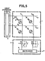
- FIG. 1 represents the diagram of an embodiment of the photosensitive device according to the invention.
- This device comprises a photosensitive matrix 1 comprising a network of horizontal connections or lines and a network of vertical connections or columns.
- FIG. 1 only a 2x2 matrix has been shown to explain the operation of the device, with two rows Lp and Lp +1 and two columns Ci and C 2 .
- the lines and the columns cross, without being of course in contact, and a photosensitive element connects each line and each column which cross.
- each photosensitive element consists of the series connection of a capacitor G, of a photodiode D, made of amorphous silicon for example, and of an electronic switch I.
- the invention applies regardless of the respective position of the components forming part of the photosensitive element.
- the device of FIG. 1 also includes an addressing circuit 2, the outputs of which are connected to the rows of the matrix, and a reading and multiplexing circuit 3, the inputs of which are connected to the columns of the matrix.
- FIG. 1 shows an embodiment of the reading and multiplexing circuit 3 in which each column of the matrix is connected to the negative input of an operational amplifier 4 whose positive input is at a constant voltage which may be the mass of the device.
- These amplifiers are mounted as integrators and have a capacitance C 'connected between their negative input and their output.
- a switch i is mounted in parallel on each capacitor C 'to ensure its reset.
- the outputs of the amplifiers are connected to a multiplexer 5, of the network of switches or CCD type for example, the output of which supplies the output signal S of the device.
- the operational amplifiers mounted as integrators copy the polarization of their positive input on their negative input.
- the positive input of the amplifiers is at a constant voltage, for example at the ground of the device.
- These amplifiers therefore connect the columns which are connected to their negative input to ground.
- a photosensitive element of the device of Figure 1 for example the element located at the intersection of the column Ci and the p th line Lp of the matrix.
- a voltage pulse V P1 is applied to all of the rows of the matrix via the addressing circuit.
- the amplitude of signal Vp goes from 0 to Vp l and at time t 2 , the amplitude of signal Vp goes from V P1 to O.
- the voltage at point A follows, after charging the capacity G, the voltage variation occurring on the lines, that is to say that from the instant ti, VA increases then stabilizes at the value V c which is the elbow or threshold voltage of the photodiode D, which directly polarizes the diode D, the cathode of which is connected to ground by the switch 1 which is on.
- any type of photodiode D can be used, for example a PIN, PN or Schottky type photodiode.
- the arrival of the pulse V P1 causes the circulation of a current corresponding to a charge Qi - Figure 2e.
- V P1 returns to zero and the voltage VA becomes negative and equal to where C G is the value of the capacitance G and where C D represents the capacitance of the photodiode D.
- C G 10 C D.
- the photodiode then works in vidicon mode and will be able to detect the light. It generates from time t 2 a dark current I OBS1 of which a fraction equal to is injected into the column.
- the device receives the light signal to be analyzed h s.
- the application of this light flash has been represented symbolically in FIG. 2a.
- This flash creates a photocurrent in photodiode D which will tend to return to zero voltage.
- the voltage VA increases slightly from ts.
- Q the amount of charge created and separated in photodiode D. The fraction is injected into the column.
- Photodiode D generates a dark current I OBS2 which is no longer injected into the column but which accumulates at point B.
- the potential of point B begins to decrease with a slope equal to I OBS2 / C D.
- the maximum charge it can store is 2Vc.CD.
- the potential of point A as a first approximation remains constant.
- This phase 0 6 marks the beginning of the reading of the line Lp.
- Point B is again connected to ground and then injects into the column a quantity of charges Q 6 corresponding to the fraction of the charge of darkness stored by point B during phase 5.
- Vp 2 of amplitude greater than that of V P1 is applied to the p th line and to it alone.
- the potential of point A increases and stabilizes at V c when photodiode D conducts. Due to the directing of photodiode D, there is circulation of a quantity of charge Q 7 of sign opposite to that of charges Q 2 , Q 3 , Q 4 , Q 6 and of the same sign as Qi and Qs .
- the charge quantity Q7 contains the signal information in the same way as Q 3 . It should be noted that Q 3 cannot be used because the light flash is sent simultaneously to the entire device and all the photodiodes flow simultaneously on the columns which provide the average value of the light signal applied.
- the signal information will be obtained from the load Q 7 .
- the device according to the invention comprises photosensitive elements each having a capacity, a photodiode and a switch. There is therefore no direct current flowing through the photosensitive elements.
- the fraction of the dark current I OBS2 equal to which is injected at the instant ts in the form of the charge Q 6 and which corresponds to the accumulation of the dark current from t 5 to ts while the lines Li to Lp- 1 were being read.
- This current is poured out at time t 7 and is compensated for by making the sum Q 6 + Q 7 .
- the reading and multiplexing circuit reads each photodiode of the selected line by summing the charges which circulate, starting before the switches of the selected line are closed and ending while the pulse Vp 2 is applied to the selected line.
- the sum Q 6 + Q7 shows that it only intervenes during phase 3 corresponding to signal illumination and during safety phases 2 and 4, the duration of which may be short compared to that of phase 5.
- V P2 of amplitude greater than V P1 displaces the average value of the point of polarization of the photodiode in direct in a zone where its dynamic resistance is weaker, and thus accelerates the phenomenon of return towards the value of balance.
- Phase 6 can be deleted.
- the quantity of charge which circulates when the line voltage changes to V P2 is then equal to Qs + Q 7 .
- the switches are closed simultaneously with the transition to V P2 .
- V P2 returns to zero.
- VA voltage
- the reading and multiplexing circuit ensures the reading of each photodiode of the selected line by summing the charges which circulate starting before the switches of the selected line are closed, continuing while the pulse V P2 is applied to the selected line, and ending while the V P2 pulse has returned to zero.
- the P th line is read by opening the switch i on the feedback of the integrating amplifiers just before phase 6. The summation of the charges is then started. The charges can be read using the muliplexer, when the integrating amplifiers have summed the charges Q 6 + Q 7 or Q 6 + Q 7 + Q 8 or Q 6 + Q 7 + Q 8 + Q 9 . Then, the switches i are closed, so as to reset the capacities of the integrators to zero before the arrival of the charges coming from the line p + 1.
- the entire device is generally illuminated simultaneously, so we have to choose an average value for Qa and for Q 9 .
- Phase 11 is called the photodiodes reset phase.
- the scintillator placed in front of the device is opaque, the rear face of the panel can be lit.
- the substrate on which the photosensitive device is made must therefore be transparent.
- the quantity of charges Q 11 can also be produced by applying a voltage pulse to the lines which pushes the photodiodes D in reverse beyond their breakdown voltage, while remaining within the limits of reversible breakdown, so as to cause circulation. of a quantity of charges Q 11 sufficient to satisfy the inequality cited above in the case of a reset by optical means.
- Phase 12 is a phase that separates an imaging cycle from the following cycle. There is circulation of a quantity of charge Qi 2 .
- phase 1 begins with the application of a voltage pulse V P1 to all the lines of the device.
- the charge Q 1 which circulates evacuates the excess of charges which could have been provided during phase 11. It is therefore not necessary to precisely calibrate this charge Q 11 .
- the switches can be left open. Current accumulates at point B. It is then necessary to close the switches before reading of the device begins to authorize the signal charges to be discharged on the rows and the columns.
- the switches of the device must be closed during phases 0 1 and 0 4, while during phases 0 2 and 0 3 , they can be either open or closed.
- the switches of the device can be closed or open either during phases les 10 to ⁇ 12 .
- the preferred solution is to leave the switches closed during phases 10, 11 and 12, and even from phase 10 to the end of phase 4 of the following imaging cycle.
- switches I can be used in series in each photosensitive element.
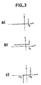
- FIG. 4 represents an embodiment where each switch I is constituted by a transistor T.
- a transistor T One can use for example a TFT in amorphous silicon, a MOSFET or a JFET.
- each switch consists of two diodes mounted head to tail, di and d 2 .
- the capacitance C D of the photodiode must be much greater than the sum of the capacitances C d i and C d2 of the two diodes.
- Vc threshold voltage
- the switch is closed, while it is open for voltages higher than + Vc and lower than - Vc.
- this switch is controlled by modulating the potential of the lines of 2Vc.
- the diodes di and d 2 have a constant capacity as a function of the voltage V, when the latter is less than Vc, as shown in FIG. 3b.
- diodes d 1 and d 2 are PIN diodes.
- FIG. 6 represents the timing diagram of the device of FIG. 5, the operation of which is little different from that of FIG. 1.
- Diode d 1 and photodiode D are forward biased by voltage V P1 . Consequently, during the application of the voltage V P1 , the voltage VA is fixed at 2Vc and the voltage V B at Vc, if it is assumed that Vc is the threshold voltage of the diodes D, di and d 2 .
- a voltage equal to 2Vc is sent to the lines.
- the voltage VA remains substantially constant but undergoes an increase of 2Vc at time ts.
- the voltage V B goes to + Vc at time t 5 to then decrease, with a slope equal to I OBS2 / CD .
- the switches of the line Lp are closed by bringing the potential of this line to zero.
- the potential V B is fixed at - Vc.
- the voltage VA stabilizes at 2Vc and the voltage V B at Vc.
- Point B varies from 2Vc and goes to - Vc and point A varies from from 2Vc.
- This capacity can be moderate and allows the design of a relatively simple reading and multiplexing circuit.
- this device does not require, as when the switches are constituted by transistors, an additional network of lines to control the transistors.
- Figures 7, 8a, b and c, and 9 relate to a technological embodiment of the device of Figure 5, and more particularly of a photosensitive element of this device.
- Figure 7 is a top view of the photosensitive element thus produced, and Figures 8a to c are sectional views along the planes AA ', BB' and CC ' of this device.
- the transparent substrate on which the photosensitive elements are made is designated by the reference 6.
- This substrate carries a first conductive level 7 which is used to make the columns, the contact with the columns of the diode di - figure 8a - and the contact at point B of the diode D with the diodes di and d 2 - figures 8a and b.
- the first conductive level 7 In the case where the optical reset is carried out through the substrate, the first conductive level 7 must be transparent.
- a PIN layer is deposited and etched so as to produce the diodes di, d 2 and D.
- the diodes d i and d 2 and D are delimited by dotted lines.
- An insulating layer 8 is deposited which serves in the part where it covers the diode D to constitute the capacitor G and which also serves to isolate the passage from the second conductive level 9.
- the following four contacts are opened: a contact on d i , figure 8a - a contact on d 2 , figure 8b - a contact on the column to connect d 2 - a contact on the contact located under the diode D to connect the diode d i to the diode D.
- the second conductive level 9 is deposited and etched to connect the diode di to point B - figure 8a, to connect the diode d 2 to the column - figure 8b and to make the lines.
- This second conducting level 9 must be transparent to the light radiation to be analyzed.
- FIG. 8c it can be seen that a photosensitive element such as those represented in FIG. 5 has not been produced exactly, but a photosensitive element such as that represented in FIG. 9.
- each photosensitive element constituted by the series connection of a capacitance G, of a diode D and of two diodes d i and d 2 mounted head to tail, a capacitance G 'in series with a diode D '.
- the capacity of the assembly constituted by the capacity G ′ and the diode D ′ in series is less than or equal to the capacity that a simple insulator would have presented.
- the probability of fault by short-circuit is lower due to the diode D 'which is reverse biased if the capacitance G' is in short-circuit.
- switches 1 in FIG. 1 could be constituted by a transistor or by two diodes mounted head to tail.
- the switches 1 can also consist of multi-layer elements of the NIN or PIP type.
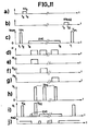
- FIG. 10 represents an embodiment of the addressing circuit for lines 2 which is represented in FIGS. 1, 4 and 5.
- This circuit comprises a logic shift register 11, controlled by at least one clock H.
- this register comprises six outputs Ri to Rs.
- Transistors h to Is are controlled by the outputs Ri to Rs and connected between a voltage V 1 and an output of the addressing circuit Si to Ss. Between each output of the circuit and a voltage Vcom, a King resistor is connected to Ro5 which imposes the voltage Vcom on the outputs of the circuit connected to lines that are not read.
- FIG. 11 is a timing diagram relating to the device of FIG. 10.
- Figure 11a concerns signal illumination.
- the light signal to be analyzed hvs which is applied between the instants ts and t 4 has been represented symbolically.
- V com is shown in FIG. 11 c.
- This voltage V com is made up of the different voltages to be applied to the lines when they are not read.
- the voltage V com comprises a voltage pulse Vpi from ti to t 2 , and a voltage equal to 2Vc from t 4 to ts. During the rest of the time, the voltage Vcom is at zero, that is to say to ground.
- FIG. 11 d shows the clock signal H of the shift register 11 of FIG. 10.
- FIGS. 11e, f and g show that each clock pulse of the signal H causes the output of the register to go high.
- Figure 11h shows the signal Vi.
- This signal Vi is formed by the different voltages to be applied to a line to read it.
- This signal Vi is at level O, and while one of the outputs of the register Ri, R 2 ... R 5 goes high, the signal V i generates a voltage pulse V P2 .
- FIG. 11 i the voltages are shown on the output Si which controls the line Li of the device.
- the transistor I 1 As long as the signal Ri is not at the high level, the transistor I 1 is blocked and the restoring resistance imposes the voltage Vcom on the output Si. It can be seen in FIG. 11 i that as long as the signal Ri is at the low level , the voltage V c om is imposed on the output Si. When the signal Ri is at the high level, the voltage Vi is found on the output Si.
- a transistor Ji to J 5 in parallel on the restoring resistors.
- the transistors J i to Js are of the same type as the transistors I 1 to I s but they are controlled by the following output of the register.
- the transistor Ji is controlled by the output R 2
- the transistor J 2 is controlled by the output Ra ...
- transistors I 1 to I 5 and J i to J s of the same type but by controlling the transistors J 1 to J s by the complementary outputs of the register.
- the transistor I 1 is controlled by the output Ri and the transistor J i by the complementary output R 1 and so on.
- transistors I 1 to I 5 and J 1 to J s which are complementary.
- the transistors I 1 and J 1 are controlled by the same output of the register, the same for the transistors 1 2 and J 2 ...
- the transistor 1 1 is passing, while the transistor Ji is blocked.
- the transistors used can be MOS transistors or TFT for example.
- FIG. 11j represents the control signal of the switches i ensuring the reset to zero when the capacities C ′ linked to the operational amplifiers 4 are high.
- the voltages delivered by the addressing circuit are defined to within a constant due to the capacitance G which is part of each photosensitive element.
- point B decreases with a slope equal to I OBS2 / C D from + Vc in the case of a switch constituted by two diodes mounted head to tail.
- the maximum charge that point B can store is equal to 2Vc Co, after which point B is at - Vc and the switch I is closed.
- the voltage V com is constituted by an increasing ramp of slope I mean OBS2 / C D , I mean OBS2 being an average value of the current I OBS2 .
- This ramp starts from + Vc at time t 4 so as to bring point B to zero at time t 4 .
- point B is at - V c at time t 4 .
- Figure 12d is similar to Figure 11d, but Figure 12e which represents the signal V 1 differs from Figure 11 h because between two voltage pulses Vp 2 the voltage does not return to zero.
- the voltage pulses V P2 are carried by a ramp which starts from zero at time t 4 and then increases with a slope equal to I mean OBS2 / C D.
- FIG. 12f shows the signal of the output S 2 of the addressing circuit of FIG. 10.
- the signal Vi is found on the output S 2 .
- the signal V com is at again applied to output S 2 .
- the use of a signal Vi such as that of FIG. 12e makes it possible to reduce the offset when passing from the voltage Vi to the voltage V co m. Now the voltage V com is calculated so that point B is close to zero.
- the signal Vi is superimposed on a ramp which starts from O whereas the signal Vcom is superimposed on a ramp which starts from V c so that there is a voltage offset at tg allowing the return of point B from Vc to zero .
- Figures 12g and 12h show the voltages VA and V B at two points A and B of the line controlled by the output S 2 .
- Vcom signals Vcom signals
- the voltages Vcom and Vi are carried by an increasing ramp of slope equal to I mean OBS2 / Co, where I mean OBS2 is an average value of the dark current of the photodiodes, so as to bring the point B to an average zero voltage.
- FIGS. 1 and 2 We have seen in the description of FIGS. 1 and 2 an embodiment of the reading and multiplexing circuit 3.
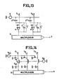
- FIG. 13 shows an embodiment in which the negative inputs of the amplifiers are connected via a capacitor C "to a generator G providing a compensation signal which makes it possible to adjust the average voltage at the output of the amplifiers 4.
- this circuit is used to generate the different voltages to be applied to the lines which are not read.
- This voltage shown in FIG. 11 c is called V com .
- This signal Vcom is applied to the positive input of amplifiers 4. It is known that these amplifiers copy the voltage existing on their positive input on their negative input.
- the addressing circuit provides a constant voltage, which can be equal to the mass, except during the time intervals where it provides the voltages to be applied to the lines to be read. In the embodiments of the addressing circuit of FIGS. 10 and 11, it is then necessary to replace the voltage V com by a constant voltage which can be the mass of the device.
- FIG. 14 represents a particular embodiment of the addressing and multiplexing circuit 3.
- FIG. 15 represents the timing diagram of the device of FIG. 14.
- This embodiment eliminates the use of operational amplifiers which are bulky and consume a lot of current.
- Figures 15a to h there is shown a series of elements of the device of Figure 14, that is to say a transistor T R , then a transistor T c and a capacitor C ST .
- a column Ci connected to a photosensitive element of the type of FIG. 5.
- the MOS transistors used are, for example, with N channel.
- the capacitance Cs T is , for example, a MOS capacity.
- Figures 15b to h show the evolution over time of the surface potential in the substrate. The conventions used are those of charge transfer devices. In particular, the crossing surface potentials are directed downwards.
- the transistors T R are blocked - see FIG. 15c.
- the excess charges are removed on the columns - see FIG. 15d - by increasing the voltage applied to the gates of the transistors T c .
- the potential of the columns is fixed at a value V clam p close to the voltage V G1 applied to the gates of the transistors Tc - see figure 15e -
- a quantity of charges Qo is transferred to each capacity C ST . This transfer can take place before or after the loads to be read arrive on the columns.
- the quantity of charges Q o is used to implement the so-called "fill and spill” technique which is used and also serves as a training charge.
Landscapes
- Engineering & Computer Science (AREA)
- Multimedia (AREA)
- Signal Processing (AREA)
- Transforming Light Signals Into Electric Signals (AREA)
- Solid State Image Pick-Up Elements (AREA)
- Image Input (AREA)
Claims (34)
Applications Claiming Priority (2)
| Application Number | Priority Date | Filing Date | Title |
|---|---|---|---|
| FR8601054A FR2593987B1 (fr) | 1986-01-24 | 1986-01-24 | Dispositif photosensible a l'etat solide |
| FR8601054 | 1986-01-24 |
Publications (2)
| Publication Number | Publication Date |
|---|---|
| EP0237365A1 EP0237365A1 (de) | 1987-09-16 |
| EP0237365B1 true EP0237365B1 (de) | 1990-10-03 |
Family
ID=9331478
Family Applications (1)
| Application Number | Title | Priority Date | Filing Date |
|---|---|---|---|
| EP87400099A Expired - Lifetime EP0237365B1 (de) | 1986-01-24 | 1987-01-16 | Lichtempfindliche Vorrichtung |
Country Status (5)
| Country | Link |
|---|---|
| US (1) | US4827145A (de) |
| EP (1) | EP0237365B1 (de) |
| JP (1) | JPS62202684A (de) |
| DE (1) | DE3765272D1 (de) |
| FR (1) | FR2593987B1 (de) |
Cited By (10)
| Publication number | Priority date | Publication date | Assignee | Title |
|---|---|---|---|---|
| US7588332B2 (en) | 2003-08-15 | 2009-09-15 | Pixel Optics | Enhanced electro-active lens system |
| US7926940B2 (en) | 2007-02-23 | 2011-04-19 | Pixeloptics, Inc. | Advanced electro-active optic device |
| US8029134B2 (en) | 1999-07-02 | 2011-10-04 | E-Vision, Llc | System, apparatus, and method for correcting vision using an electro-active lens |
| US8337014B2 (en) | 2006-05-03 | 2012-12-25 | Pixeloptics, Inc. | Electronic eyeglass frame |
| US8408699B2 (en) | 2006-06-23 | 2013-04-02 | Pixeloptics, Inc. | Electro-active spectacle lenses |
| US8641191B2 (en) | 1999-07-02 | 2014-02-04 | E-Vision, Llc | Static progressive surface region in optical communication with a dynamic optic |
| US8778022B2 (en) | 2004-11-02 | 2014-07-15 | E-Vision Smart Optics Inc. | Electro-active intraocular lenses |
| US8915588B2 (en) | 2004-11-02 | 2014-12-23 | E-Vision Smart Optics, Inc. | Eyewear including a heads up display |
| US9122083B2 (en) | 2005-10-28 | 2015-09-01 | E-Vision Smart Optics, Inc. | Eyewear docking station and electronic module |
| US9155614B2 (en) | 2007-01-22 | 2015-10-13 | E-Vision Smart Optics, Inc. | Flexible dynamic electro-active lens |
Families Citing this family (56)
| Publication number | Priority date | Publication date | Assignee | Title |
|---|---|---|---|---|
| FR2626128B1 (fr) * | 1988-01-15 | 1990-05-04 | Thomson Csf | Matrice photosensible a deux diodes et une capacite par point, sans remise a niveau optique |
| FR2627922B1 (fr) * | 1988-02-26 | 1990-06-22 | Thomson Csf | Matrice photosensible a deux diodes par point, sans conducteur specifique de remise a niveau |
| FR2634947B1 (fr) * | 1988-07-29 | 1990-09-14 | Thomson Csf | Matrice photosensible a deux diodes de meme polarite et une capacite par point photosensible |
| GB2222249B (en) * | 1988-08-24 | 1992-07-08 | Rosemount Ltd | Optical sensor |
| DE4002431A1 (de) * | 1990-01-27 | 1991-08-01 | Philips Patentverwaltung | Sensormatrix |
| GB9220104D0 (en) | 1992-09-07 | 1992-11-04 | Philips Electronics Uk Ltd | Matrix display device with light sensing function |
| GB9226890D0 (en) * | 1992-12-23 | 1993-02-17 | Philips Electronics Uk Ltd | An imaging device |
| GB9301405D0 (en) * | 1993-01-25 | 1993-03-17 | Philips Electronics Uk Ltd | An image sensor |
| GB9314402D0 (en) * | 1993-07-12 | 1993-08-25 | Philips Electronics Uk Ltd | An imaging device |
| US5410145A (en) * | 1994-02-25 | 1995-04-25 | Coroy; Trenton G. | Light detector using reverse biased photodiodes with dark current compensation |
| DE4429434C1 (de) * | 1994-08-19 | 1995-12-21 | Siemens Ag | Bildsensor |
| FR2731569B1 (fr) * | 1995-03-07 | 1997-04-25 | Thomson Tubes Electroniques | Dispositif de recopie de tension a grande linearite |
| DE19524856A1 (de) * | 1995-07-07 | 1997-01-09 | Siemens Ag | Röntgenbilderzeugungssystem |
| US5818898A (en) * | 1995-11-07 | 1998-10-06 | Kabushiki Kaisha Toshiba | X-ray imaging apparatus using X-ray planar detector |
| US5652430A (en) * | 1996-05-03 | 1997-07-29 | Sterling Diagnostic Imaging, Inc. | Direct radiographic imaging panel |
| US5668375A (en) * | 1996-08-26 | 1997-09-16 | General Electric Company | Fast scan reset for a large area x-ray detector |
| FR2760585B1 (fr) * | 1997-03-07 | 1999-05-28 | Thomson Tubes Electroniques | Procede de commande d'un dispositif photosensible a faible remanence, et dispositif photosensible mettant en oeuvre le procede |
| JP4098884B2 (ja) * | 1998-07-08 | 2008-06-11 | 浜松ホトニクス株式会社 | 固体撮像装置 |
| JP2001056382A (ja) * | 1999-06-07 | 2001-02-27 | Toshiba Corp | 放射線検出器及び放射線診断装置 |
| US6857741B2 (en) | 2002-01-16 | 2005-02-22 | E-Vision, Llc | Electro-active multi-focal spectacle lens |
| US6491391B1 (en) | 1999-07-02 | 2002-12-10 | E-Vision Llc | System, apparatus, and method for reducing birefringence |
| US7023594B2 (en) | 2000-06-23 | 2006-04-04 | E-Vision, Llc | Electro-optic lens with integrated components |
| US6871951B2 (en) | 2000-06-23 | 2005-03-29 | E-Vision, Llc | Electro-optic lens with integrated components |
| US6986579B2 (en) | 1999-07-02 | 2006-01-17 | E-Vision, Llc | Method of manufacturing an electro-active lens |
| US6733130B2 (en) | 1999-07-02 | 2004-05-11 | E-Vision, Llc | Method for refracting and dispensing electro-active spectacles |
| US6491394B1 (en) | 1999-07-02 | 2002-12-10 | E-Vision, Llc | Method for refracting and dispensing electro-active spectacles |
| US6517203B1 (en) | 1999-07-02 | 2003-02-11 | E-Vision, Llc | System, apparatus, and method for correcting vision using electro-active spectacles |
| US7264354B2 (en) | 1999-07-02 | 2007-09-04 | E-Vision, Llc | Method and apparatus for correcting vision using an electro-active phoropter |
| US7404636B2 (en) | 1999-07-02 | 2008-07-29 | E-Vision, Llc | Electro-active spectacle employing modal liquid crystal lenses |
| US6851805B2 (en) | 1999-07-02 | 2005-02-08 | E-Vision, Llc | Stabilized electro-active contact lens |
| US7604349B2 (en) | 1999-07-02 | 2009-10-20 | E-Vision, Llc | Static progressive surface region in optical communication with a dynamic optic |
| US7775660B2 (en) | 1999-07-02 | 2010-08-17 | E-Vision Llc | Electro-active ophthalmic lens having an optical power blending region |
| FR2796239B1 (fr) * | 1999-07-06 | 2001-10-05 | Trixell Sas | Procede de commande d'un dispositif photosensible apte a produire des images de bonne qualite |
| FR2802698B1 (fr) * | 1999-12-17 | 2002-03-22 | Trixell Sas | Circuit de lecture de charges protege contre des surcharges provenant de charges de polarite non desiree |
| JP3984808B2 (ja) | 2000-09-07 | 2007-10-03 | キヤノン株式会社 | 信号処理装置及びそれを用いた撮像装置並びに放射線撮像システム |
| US9801709B2 (en) | 2004-11-02 | 2017-10-31 | E-Vision Smart Optics, Inc. | Electro-active intraocular lenses |
| AU2005302202B2 (en) | 2004-11-02 | 2012-04-05 | E-Vision, Llc | Electro-active spectacles and method of fabricating same |
| US8885139B2 (en) | 2005-01-21 | 2014-11-11 | Johnson & Johnson Vision Care | Adaptive electro-active lens with variable focal length |
| WO2008105780A2 (en) | 2006-05-24 | 2008-09-04 | Pixeloptics, Inc. | Optical rangefinder for an electro-active lens |
| WO2007146853A2 (en) | 2006-06-12 | 2007-12-21 | Johnson & Johnson Vision Care, Inc. | Method to reduce power consumption with electro-optic lenses |
| MX2009008829A (es) | 2007-02-23 | 2011-10-28 | Pixeloptics Inc | Apertura dinamica oftalmica. |
| US20080273169A1 (en) | 2007-03-29 | 2008-11-06 | Blum Ronald D | Multifocal Lens Having a Progressive Optical Power Region and a Discontinuity |
| US7883206B2 (en) | 2007-03-07 | 2011-02-08 | Pixeloptics, Inc. | Multifocal lens having a progressive optical power region and a discontinuity |
| US7883207B2 (en) | 2007-12-14 | 2011-02-08 | Pixeloptics, Inc. | Refractive-diffractive multifocal lens |
| US12572035B2 (en) | 2007-05-04 | 2026-03-10 | E-Vision Optics, Llc | Moisture-resistant eye wear |
| US11061252B2 (en) | 2007-05-04 | 2021-07-13 | E-Vision, Llc | Hinge for electronic spectacles |
| US10613355B2 (en) | 2007-05-04 | 2020-04-07 | E-Vision, Llc | Moisture-resistant eye wear |
| US8317321B2 (en) | 2007-07-03 | 2012-11-27 | Pixeloptics, Inc. | Multifocal lens with a diffractive optical power region |
| DE102007050253A1 (de) * | 2007-10-20 | 2009-04-23 | Dr. Johannes Heidenhain Gmbh | Detektorelement-Array für eine optische Positionsmesseinrichtung |
| US8154804B2 (en) | 2008-03-25 | 2012-04-10 | E-Vision Smart Optics, Inc. | Electro-optic lenses for correction of higher order aberrations |
| KR101078396B1 (ko) * | 2008-09-08 | 2011-11-01 | (주)에프에스디글로벌 | 이미지 센서, 이의 제조방법 및 이를 포함하는 사무기기 |
| US12436411B2 (en) | 2010-07-02 | 2025-10-07 | E-Vision Optics, Llc | Moisture-resistant eye wear |
| US12510773B2 (en) | 2011-02-11 | 2025-12-30 | E-Vision Optics, Llc | Moisture-resistant eye wear |
| FR3029054B1 (fr) | 2014-11-24 | 2018-01-26 | Commissariat A L'energie Atomique Et Aux Energies Alternatives | Controle de la duree d'integration dans un dispositif photosensible |
| ES2973138T3 (es) | 2016-04-12 | 2024-06-18 | E Vision Smart Optics Inc | Lentes electroactivas con puentes resistivos elevados |
| US10599006B2 (en) | 2016-04-12 | 2020-03-24 | E-Vision Smart Optics, Inc. | Electro-active lenses with raised resistive bridges |
Family Cites Families (5)
| Publication number | Priority date | Publication date | Assignee | Title |
|---|---|---|---|---|
| US3521244A (en) * | 1968-10-23 | 1970-07-21 | Rca Corp | Electrical circuit for processing periodic signal pulses |
| DE2939490A1 (de) * | 1979-09-28 | 1981-04-16 | Siemens AG, 1000 Berlin und 8000 München | Monolithisch integrierter zweidimensionaler bildsensor mit einer differenzbildenden stufe |
| FR2487566A1 (fr) * | 1980-07-25 | 1982-01-29 | Thomson Csf | Matrice de detection d'un rayonnement electromagnetique et intensificateur d'images radiologiques comportant une telle matrice |
| JPS5942511B2 (ja) * | 1982-04-13 | 1984-10-15 | 株式会社東芝 | 密着センサ |
| US4686373A (en) * | 1983-08-31 | 1987-08-11 | Texas Instruments Incorporated | Infrared imager |
-
1986
- 1986-01-24 FR FR8601054A patent/FR2593987B1/fr not_active Expired
-
1987
- 1987-01-16 EP EP87400099A patent/EP0237365B1/de not_active Expired - Lifetime
- 1987-01-16 DE DE8787400099T patent/DE3765272D1/de not_active Expired - Fee Related
- 1987-01-20 US US07/005,080 patent/US4827145A/en not_active Expired - Fee Related
- 1987-01-23 JP JP62013891A patent/JPS62202684A/ja active Pending
Cited By (16)
| Publication number | Priority date | Publication date | Assignee | Title |
|---|---|---|---|---|
| US9323101B2 (en) | 1999-07-02 | 2016-04-26 | E-Vision Smart Optics, Inc. | Electro-active opthalmic lens having an optical power blending region |
| US9500883B2 (en) | 1999-07-02 | 2016-11-22 | E-Vision Smart Optics, Inc. | Electro-active opthalmic lens having an optical power blending region |
| US8029134B2 (en) | 1999-07-02 | 2011-10-04 | E-Vision, Llc | System, apparatus, and method for correcting vision using an electro-active lens |
| US8641191B2 (en) | 1999-07-02 | 2014-02-04 | E-Vision, Llc | Static progressive surface region in optical communication with a dynamic optic |
| US9411173B1 (en) | 1999-07-02 | 2016-08-09 | E-Vision Smart Optics, Inc. | Electro-active opthalmic lens having an optical power blending region |
| US7588332B2 (en) | 2003-08-15 | 2009-09-15 | Pixel Optics | Enhanced electro-active lens system |
| US8778022B2 (en) | 2004-11-02 | 2014-07-15 | E-Vision Smart Optics Inc. | Electro-active intraocular lenses |
| US8915588B2 (en) | 2004-11-02 | 2014-12-23 | E-Vision Smart Optics, Inc. | Eyewear including a heads up display |
| US8931896B2 (en) | 2004-11-02 | 2015-01-13 | E-Vision Smart Optics Inc. | Eyewear including a docking station |
| US9124796B2 (en) | 2004-11-02 | 2015-09-01 | E-Vision Smart Optics, Inc. | Eyewear including a remote control camera |
| US9122083B2 (en) | 2005-10-28 | 2015-09-01 | E-Vision Smart Optics, Inc. | Eyewear docking station and electronic module |
| US8337014B2 (en) | 2006-05-03 | 2012-12-25 | Pixeloptics, Inc. | Electronic eyeglass frame |
| US8408699B2 (en) | 2006-06-23 | 2013-04-02 | Pixeloptics, Inc. | Electro-active spectacle lenses |
| US9155614B2 (en) | 2007-01-22 | 2015-10-13 | E-Vision Smart Optics, Inc. | Flexible dynamic electro-active lens |
| US7926940B2 (en) | 2007-02-23 | 2011-04-19 | Pixeloptics, Inc. | Advanced electro-active optic device |
| US8708483B2 (en) | 2007-05-04 | 2014-04-29 | Pixeloptics, Inc. | Electronic eyeglass frame |
Also Published As
| Publication number | Publication date |
|---|---|
| FR2593987A1 (fr) | 1987-08-07 |
| EP0237365A1 (de) | 1987-09-16 |
| JPS62202684A (ja) | 1987-09-07 |
| FR2593987B1 (fr) | 1989-08-04 |
| DE3765272D1 (de) | 1990-11-08 |
| US4827145A (en) | 1989-05-02 |
Similar Documents
| Publication | Publication Date | Title |
|---|---|---|
| EP0237365B1 (de) | Lichtempfindliche Vorrichtung | |
| EP0028960B1 (de) | Strahlungsdetektorenmatrix und Röntgenbild-Verstärker mit einer solchen Matrix | |
| FR2593343A1 (fr) | Matrice d'elements photosensibles et son procede de fabrication, procede de lecture associe, et application de cette matrice a la prise de vue d'images | |
| FR2598250A1 (fr) | Panneau de prise de vue radiologique, et procede de fabrication | |
| EP3386186B1 (de) | Bilderfassungssensor | |
| FR2736460A1 (fr) | Circuits de memorisation de tension | |
| EP0331546B1 (de) | Photoempfindlicher Matrix mit zwei Dioden pro Punkt ohne spezifischen Rückstellungsleiter | |
| EP0965224B1 (de) | Verfahren zur steuerung einer lichtempfindlichen vorrichtung mit schwacher remanenz und lichtempfindliche vorrichtung zur durchführung des verfahrens | |
| EP1156491A2 (de) | Verbesserungen an Schieberegistern unter alleiniger Verwendung von "MIS" Transistoren | |
| EP0491596A1 (de) | Monolitischer Infrarotdetektor aus pyroelektrischem Material | |
| EP1673932B1 (de) | Steuerverfahren für eine lichtempfindliche einrichtung | |
| EP0357468B1 (de) | Photoempfindliche Matrix mit zwei Dioden gleicher Polarität und einer Kapazität pro photoempfindlichem Punkt | |
| FR2513015A1 (fr) | Dispositif de detection d'image en couleurs du type transfert de charge | |
| FR2591409A1 (fr) | Camera thermique a balayage parallele | |
| CA2449939C (fr) | Procede de commande d'un dispositif photosensible | |
| EP0749234B1 (de) | Halbleiter-Bildsensor mit integrierte Pixelhistogrammumwandlung | |
| FR2705183A1 (fr) | Structure améliorée d'adressage à diodes pour adressage d'un réseau de transducteurs. | |
| EP0275740B1 (de) | Ausleseschaltung für eine lichtempfindliche Zeilenübertragungsanordnung, lichtempfindliche Zeilenübertragungsanordnung mit einer solchen Schaltung und Ausleseverfahren einer solchen Anordnung | |
| FR2759509A1 (fr) | Circuit integrateur a linearite amelioree | |
| WO2001003419A1 (fr) | Procede de commande d'un dispositif photosensible apte a produire des images de bonne qualite | |
| FR2626128A1 (fr) | Matrice photosensible a deux diodes et une capacite par point, sans remise a niveau optique | |
| WO1999035820A1 (fr) | Dispositif de prise de vue a transfert de charges sur un element de connexion | |
| EP0217691A1 (de) | Abtastung und Halteschaltung mit Diodenbrücke |
Legal Events
| Date | Code | Title | Description |
|---|---|---|---|
| PUAI | Public reference made under article 153(3) epc to a published international application that has entered the european phase |
Free format text: ORIGINAL CODE: 0009012 |
|
| AK | Designated contracting states |
Kind code of ref document: A1 Designated state(s): DE GB NL |
|
| 17P | Request for examination filed |
Effective date: 19871116 |
|
| RAP3 | Party data changed (applicant data changed or rights of an application transferred) |
Owner name: THOMSON-CSF |
|
| 17Q | First examination report despatched |
Effective date: 19891113 |
|
| GRAA | (expected) grant |
Free format text: ORIGINAL CODE: 0009210 |
|
| AK | Designated contracting states |
Kind code of ref document: B1 Designated state(s): DE GB NL |
|
| PG25 | Lapsed in a contracting state [announced via postgrant information from national office to epo] |
Ref country code: NL Effective date: 19901003 |
|
| REF | Corresponds to: |
Ref document number: 3765272 Country of ref document: DE Date of ref document: 19901108 |
|
| GBT | Gb: translation of ep patent filed (gb section 77(6)(a)/1977) | ||
| PG25 | Lapsed in a contracting state [announced via postgrant information from national office to epo] |
Ref country code: GB Effective date: 19910116 |
|
| NLV1 | Nl: lapsed or annulled due to failure to fulfill the requirements of art. 29p and 29m of the patents act | ||
| PLBE | No opposition filed within time limit |
Free format text: ORIGINAL CODE: 0009261 |
|
| STAA | Information on the status of an ep patent application or granted ep patent |
Free format text: STATUS: NO OPPOSITION FILED WITHIN TIME LIMIT |
|
| GBPC | Gb: european patent ceased through non-payment of renewal fee | ||
| 26N | No opposition filed | ||
| PG25 | Lapsed in a contracting state [announced via postgrant information from national office to epo] |
Ref country code: DE Effective date: 19911001 |