EP0254212B1 - MOS-Halbleiterschaltung - Google Patents
MOS-Halbleiterschaltung Download PDFInfo
- Publication number
- EP0254212B1 EP0254212B1 EP87110298A EP87110298A EP0254212B1 EP 0254212 B1 EP0254212 B1 EP 0254212B1 EP 87110298 A EP87110298 A EP 87110298A EP 87110298 A EP87110298 A EP 87110298A EP 0254212 B1 EP0254212 B1 EP 0254212B1
- Authority
- EP
- European Patent Office
- Prior art keywords
- coupled
- mos transistor
- mos
- gate
- drain
- Prior art date
- Legal status (The legal status is an assumption and is not a legal conclusion. Google has not performed a legal analysis and makes no representation as to the accuracy of the status listed.)
- Expired - Lifetime
Links
- 239000004065 semiconductor Substances 0.000 title claims description 28
- 229910021420 polycrystalline silicon Inorganic materials 0.000 claims description 20
- 229920005591 polysilicon Polymers 0.000 claims description 20
- 238000007493 shaping process Methods 0.000 claims description 9
- 230000004044 response Effects 0.000 claims description 3
- 230000000087 stabilizing effect Effects 0.000 claims 1
- 230000010355 oscillation Effects 0.000 description 21
- 238000010586 diagram Methods 0.000 description 17
- 239000003990 capacitor Substances 0.000 description 9
- 238000007599 discharging Methods 0.000 description 8
- 239000000872 buffer Substances 0.000 description 5
- 238000004519 manufacturing process Methods 0.000 description 5
- 230000001419 dependent effect Effects 0.000 description 3
- 230000000694 effects Effects 0.000 description 3
- 238000009792 diffusion process Methods 0.000 description 2
- 230000000630 rising effect Effects 0.000 description 2
- XAGFODPZIPBFFR-UHFFFAOYSA-N aluminium Chemical compound [Al] XAGFODPZIPBFFR-UHFFFAOYSA-N 0.000 description 1
- 229910052782 aluminium Inorganic materials 0.000 description 1
- 239000004411 aluminium Substances 0.000 description 1
- 230000015572 biosynthetic process Effects 0.000 description 1
- 239000000969 carrier Substances 0.000 description 1
- 239000000470 constituent Substances 0.000 description 1
- 230000007423 decrease Effects 0.000 description 1
- 230000003111 delayed effect Effects 0.000 description 1
- 230000003071 parasitic effect Effects 0.000 description 1
- 230000000737 periodic effect Effects 0.000 description 1
- 239000002699 waste material Substances 0.000 description 1
Images


Classifications
-
- G—PHYSICS
- G11—INFORMATION STORAGE
- G11C—STATIC STORES
- G11C8/00—Arrangements for selecting an address in a digital store
-
- H—ELECTRICITY
- H03—ELECTRONIC CIRCUITRY
- H03K—PULSE TECHNIQUE
- H03K3/00—Circuits for generating electric pulses; Monostable, bistable or multistable circuits
- H03K3/02—Generators characterised by the type of circuit or by the means used for producing pulses
- H03K3/353—Generators characterised by the type of circuit or by the means used for producing pulses by the use, as active elements, of field-effect transistors with internal or external positive feedback
- H03K3/354—Astable circuits
-
- H—ELECTRICITY
- H03—ELECTRONIC CIRCUITRY
- H03K—PULSE TECHNIQUE
- H03K3/00—Circuits for generating electric pulses; Monostable, bistable or multistable circuits
- H03K3/01—Details
- H03K3/011—Modifications of generator to compensate for variations in physical values, e.g. voltage, temperature
-
- H—ELECTRICITY
- H03—ELECTRONIC CIRCUITRY
- H03K—PULSE TECHNIQUE
- H03K3/00—Circuits for generating electric pulses; Monostable, bistable or multistable circuits
- H03K3/02—Generators characterised by the type of circuit or by the means used for producing pulses
- H03K3/027—Generators characterised by the type of circuit or by the means used for producing pulses by the use of logic circuits, with internal or external positive feedback
- H03K3/03—Astable circuits
- H03K3/0315—Ring oscillators
Definitions
- This invention relates to an MOS semiconductor circuit comprising: first and second voltage terminals; cascade-connected logic circuits; a first MOS transistor circuit having first MOS transistors coupled between said first voltage terminal and output nodes of respective logic circuits; a second MOS transistor having the same conductivity type as said first MOS transistor and having a source, a gate coupled to a gate of said first MOS transistors and a drain coupled to said gate of said second MOS transistor; a current control circuit, coupled to said drain of said second MOS transistor, for causing a predetermined current to flow through the source-drain path of said second MOS transistor; a second MOS transistor circuit having third MOS transistors coupled between said second voltage terminal and respective output nodes of said logic circuits; and a fourth MOS transistor having the same conductivity type as said third MOS transistors and having a gate coupled to a gate of said third MOS transistors and a drain coupled to said gate of said fourth MOS transistor.
- a device is known from US-A-4 592 087.
- a dynamic RAM needs a periodic refresh operation or data hold operation. Many of recent DRAMs automatically initiate a refresh operation when they are not accessed, i.e. when they are in a standby mode.
- This type of a RAM has a refresh timer provided on the same chip, and this refresh timer measures the time interval between refresh operations to regularly trigger the refresh operation.
- the refresh timer is constituted by a ring oscillator.
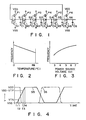
- Fig. 1 illustrates a conventional ring oscillator used as a refresh timer.
- the first five CMOS inverters I1 to I5 are coupled in ring, and the output of inverter I5 is coupled to the last CMOS inverter I6, which serves as a wave shaper.
- These inverters I1 to I6 have their respective output nodes S1 to S6 coupled to parasitic electrostatic capacitors C1 to C6, respectively.
- the ring oscillator When the ring oscillator is used as a refresh timer, its oscillation period is between, for example, 10 ⁇ s and 100 ⁇ s and its dissipation power determines the dissipation power of a DRAM in standby mode. Therefore, it is desirable to reduce the dissipation power of the ring oscillator itself as low as possible.
- each of the CMOS inverters coupled in ring e.g., P-channel MOS transistor P1 and N-channel MOS transistor N1 of inverter I1 are designed to have a long channel length L so that these transistors each have a small conductance. For instance, their channel width W is about 2 ⁇ m while the channel length L is 200 ⁇ m.
- transistors P6 and N6 constituting wave-shaping inverter I6 are designed to have a relatively large conductance; for instance, their channel width W is as wide as 100 ⁇ m.
- This wave-shaping inverter I6 drives another circuit (not shown) and electrostatic capacitor C6 coupled to its output node S6 has a capacitance as high as 5 pF.
- the aforementioned ring oscillator is used not only as the refresh timer, but also in a base-plate bias circuit that provides a base-plate bias voltage on chip.
- Figs. 2 and 3 respectively depict the temperature characteristic of the oscillation frequency and the dependency of the oscillation frequency on the power source voltage in the prior art ring oscillator. As indicated by the characteristic of Fig. 2, the oscillation frequency varies about 30-40 % between 0°C and 85°C. As should be clear from the characteristic curve of Fig. 3, the oscillation frequency also varies about 30 % when the power source voltage VDD varies between 4 V and 6 V.
- the refresh timer requires such a characteristic that the oscillation frequency is high at a high temperature and a low power source voltage.
- the prior art refresh timer actually has the contrary characteristics as shown in Figs. 2 and 3. Therefore, according to the prior art, the refresh timer is designed to have a minimum allowable frequency at a high temperature and a low power source voltage in order to ensure data holding even at these temperature and voltage levels. Consequently, the refresh timer oscillates at a higher frequency at a low temperature and a high power source voltage, thus significantly increasing the standby current.
- the refresh interval need not be short in these temperature and voltage conditions, the refresh operation is executed frequently and thus wastefully because the refresh timer oscillates at a high frequency.
- the standby current increases by 140 % (due to the temperature change) ⁇ 130 % (due to the power source voltage change) of what is necessary and becomes about 180 % of the proper amount, thus increasing the dissipation power.
- the actual standby current would be two to three times the proper standby current.
- transistors P1 and N1 of inverter I1 have a long channel length L so as to have a small conductance, the area occupied by each inverter on an integrated chip is above 10000 ⁇ m2, thus undesirably increasing the overall chip area.
- the prior art circuit has another shortcoming as follows.
- Fig. 4 shows the waveforms of the output voltages at output nodes S5 and S6 of the respective inverters I5 and I6 of the ring oscillator shown in Fig. 1.
- a variation in the output voltage of inverter I5 at node S5 is considerably gentle as compared with a variation in the output voltage of inverter I6 at node S6.
- the time interval between t1 where the output voltage at node S5 is VSS and t2 where it is increased to the threshold voltage VTN of the N-channel MOS transistor is 10 ⁇ s.
- the maximum current flowing between the voltage terminals in the ring oscillator is 5 mA and the channel widths W of transistors N6 and P6 are 100 ⁇ m and 200 ⁇ m, respectively. Then, the average current flowing in inverter I6 is 50 ⁇ A, making it difficult to attain a low dissipation power due to the presence of inverter I6.
- inverter I6 If the wave-shaping inverter I6 is omitted or the conductances of transistors P6 and N6 are reduced, the current path between the voltage terminals would disappear or the current would be reduced. However, in this case, the same phenomenon would in turn occur at the first stage of another circuit (not shown) which is driven by the output signal of inverter I6. After all, the dissipation power cannot be reduced. Although inverter I1 is also driven by the output signal of inverter I5, its conductance is as low as 1/10000 of that of the wave-shaping inverter I6 so that the current flowing between voltage terminals of inverter I1 is negligible.
- the prior art circuit has some shortcomings such that the temperature and voltage characteristics cannot be flexibly set, the dissipation power and the chip area cannot be reduced as desired, and the oscillation frequency is not stable with respect to a change in temperature, voltage and manufacturing processes.
- the semiconductor circuit initially defined is characterized in that: said current control circuit comprises a polysilicon resistor coupled between said drains of said second and fourth MOS transistors.
- an MOS semiconductor circuit comprising first and second voltage terminals; cascade-connected logic circuits; a first MOS transistor circuit having first MOS transistors coupled to said first voltage terminal in series with respective logic circuits; a second MOS transistor having the same conductivity type as said first MOS transistors and having a source, a gate coupled to a gate of said first MOS transistors and a drain coupled to said gate of said second MOS transistor; a first current control circuit, coupled to the drain of said second MOS transistor, for causing a first predetermined current to flow through the source-drain path of said second MOS transistor; a second MOS transistor circuit having third MOS transistors coupled to said second voltage terminal and in series with respective said logic circuits; a fourth MOS transistor of said current control circuit having the same conductivity type as said third MOS transistors and having a source, a gate coupled to a gate of said third MOS transistors and a drain coupled to said gate of said fourth MOS transistor; and a second current control circuit
- Fig. 5 is a circuit diagram showing the first embodiment of this invention in which an MOS semiconductor circuit of this invention is applied to a ring oscillator.
- the reference numerals used in the prior art circuit of Fig. 1 are also used for corresponding parts of Fig. 5.
- N-channel MOS transistors N11 to N15 are inserted between voltage terminal VSS and N-channel MOS transistors N1 to N5 of inverters I1 to I5, respectively.
- P-channel MOS transistors P11 to P15 are inserted between voltage terminal VDD and P-channel MOS transistors P1 to P5 of inverters I1 to I5, respectively.
- P-channel MOS transistor P16 has its source coupled to voltage terminal VDD and its gate and drain short-circuited.
- N-channel MOS transistor N16 has its source coupled to voltage terminal VSS and its gate and drain short-circuited.
- a resistor R1 formed of polysilicon is inserted between the drain of P-channel MOS transistor P16 and the drain of N-channel MOS transistor N16.
- the resistor R1 and two transistors P16 and N16 constitute a bias control circuit B1.
- a signal at output node S5 of inverter I5 is supplied to a toggle flip-flop circuit TFF through two inverters I7 and I8 serving as buffers.
- the gate and drain of transistor P16 are short-circuited and this gate is further coupled to the gates of transistors P11 to P15, while the gate and drain of transistor N16 are similarly short-circuited and this gate is further coupled to the gates of transistors N11 to N15.
- This arrangement is known as a current mirror circuit. Because transistor N16 has the same bias condition between its gate and source as, for example, transistor N11, the same current would flow in transistors N11 and N16 when these transistors have the same channel length and the same channel width.
- the bias current control means for transistor N16 is constituted by polysilicon resistor R1, and a current d1 determined by this resistor R1 equals a maximum current d2 of transistor N11. This current d2 causes discharging of electrostatic capacitor C1 coupled to output node S1.
- the temperature dependency of the oscillation frequency is explained.
- the capacitance of electrostatic capacitor C1 is hardly dependent on the temperature.
- current d1 which determines current d2 for discharging the charges accumulated in electrostatic capacitor C1
- polysilicon resistor R1 current d2 is also hardly dependent on the temperature.
- Fig. 6 shows the temperature dependency of the sheet resistance of the polysilicon resistor.
- the polysilicon resistor is significantly stable against a temperature change, and since the equivalent resistance of a transistor is determined by the amount of carriers moved, the polysilicon resistor is in a sharp contrast with the one having a large temperature dependency.
- toggle flip-flop circuit TFF is used to frequency-divided the output signal of inverter I5, thus ensuring the use of a lower oscillation frequency.
- each transistor in the conventional circuit of Fig. 1 is proportional to source voltage VDD. Therefore, the amount of charges accumulated in each electrostatic capacitor C is proportional to power source voltage VDD, which means the discharging time of electrostatic capacitor C1 is inversely proportional to power source voltage VDD. In this embodiment, however, the discharging time for each of electrostatic capacitors C1 to C5 does not depend on the equivalent resistances of transistors N1 to N5, but is proportional to current d1 flowing across resistor R1.
- this current d1 becomes a value obtained by subtracting threshold voltage VTP of p-channel MOS transistor P16 and threshold voltage VTN of N-channel MOS transistor N16 from the source voltage VDD and dividing the result by the resistance of resistor R1, the discharging time is proportional to (VDD - VTP - VTN). Assuming that threshold voltages VTP and VTN are sufficiently smaller than source voltage VDD, the discharge current and charges to be discharged are proportional to source voltage VDD. Accordingly, the discharging time is hardly dependent on the source voltage, so is the oscillation frequency, which is thus significantly improved as indicated by the solid line in Fig. 8, as compared with the conventional case that is indicated by the broken line in Fig. 8.
- Fig. 9 is a circuit diagram depicting the configuration of the second embodiment of this invention, which is designed to further reduce the source-voltage dependency.
- bias control circuits B2 and B3 are separately provided using P-channel MOS transistor P17 and N-channel MOS transistor N17, respectively.
- P-channel MOS transistor P17 has its gate and drain short-circuited and its source coupled to voltage terminal VDD, while N-channel MOS transistor N17 has its gate and drain short-circuited and its source coupled to voltage terminal VSS.
- bias control circuit B2 a polysilicon resistor R2 is inserted as a bias current control means between the drain of P-channel MOS transistor P17 and voltage terminal VSS, the gate of P-channel MOS transistor P17 is coupled to the gates of P-channel MOS transistors P11 to P15.
- bias control circuit B3 another polysilicon resistor R3 is provided, also as a bias current control means, between the drain of N-channel MOS transistor N17 and voltage terminal VSS, and the gate of transistor N17 is coupled to the gates of N-channel MOS transistors N11 to N15.
- each bias control circuit B2 or B3 includes only a single transistor and current d3 flowing across resistor R3 is proportional to (VDD - VTH), the discharging current and the amount of charges to be discharged are more faithfully proportional to power source voltage VDD.
- the Fig. 5 circuit is advantageous in that inverters I1 to I5 have the same rising characteristic.
- the P-channel MOS transistors and the N-channel MOS transistors of each inverter e.g. transistors P1 and N1, and control transistor P11 are provided in reverse order as compared with the circuit shown in Fig. 5.
- the circuit with this arrangement is otherwise substantially the same as the circuit of Fig. 5. It should be noted, however, that a current control N-channel MOS transistor is provided between voltage terminal VSS and each of output nodes S1 to S5 of inverters I1 to I5.
- the aforementioned embodiments use CMOS devices having P-channel and N-channel MOS transistors.
- Fig. 10 is a circuit diagram showing a further embodiment of this invention wherein a diode D1 is coupled, in parallel but with the reverse polarity, to resistor R1 of bias control circuit B1 of the embodiment shown in Fig. 5, thus constituting bias control circuit B5.
- circuits I1 to I5 are explained as inverters constituting a ring oscillator.
- the word "inverter” here indicates a circuit which logically performs an inverting operation when operated, and is not used in a narrow sense.
- transistors P16,N16,P19 and N19 need a small chip-occupying area, so that the chip-occupying area of the overall circuit is below one half of what is required for the conventional circuit.
- This feature solves one of the conventional problems which is concerned with the chip-occupying area.
- polysilicon resistor R1 may have to be as long as 10 mm, but this can be formed under an aluminium wire via an insulating layer so that the length does not increase the chip-occupying area.
- the oscillation frequency does not depend on a variation in manufacturing processes and is always stable.
- a variation in a polysilicon resistance is about 10 %.
- the ring oscillators of the aforementioned embodiments have a stable oscillation frequency, they do not waste the refresh current like the conventional one does and therefore realize a refresh timer with reduced dissipation power.
- transistors N16 and N11 have the same channel length, thus minimizing a deviation due to the short channel effect.
- a plurality of transistors having the same channel width need to be coupled in parallel with one another.
- Fig. 11 is a circuit diagram illustrating the configuration of a further embodiment of this invention. This embodiment is designed to prevent a formation of a current path between voltage terminals VDD and VSS due to a gradual change in the output waveform of inverter I5, which may occur in the conventional circuit.
- inverters I7 and I8 serving as buffers in the embodiment of Fig. 5 are eliminated, and NAND gate K1 and NOR gate K2, both of which receive the output signals from output nodes S5 and S2 of inverters I5 and I2 as their inputs, are provided.
- the circuit of Fig. 11 further has P-channel MOS transistor P31, having its source coupled to voltage terminal VDD, and N-channel MOS transistor N31, which has its source coupled to voltage terminal VSS and its drain coupled to the drain of transistor P31.
- transistors P31 and N31 constitute wave shaper I11, and the former transistor P31 has its gate supplied with the signal from output node S11 of NAND gate K1 and the latter one has its gate supplied with the signal from output node S12 of NOR gate K2.
- P-channel MOS transistors P32 and P33 which have their gates coupled to the gate of P-channel MOS transistor P16 of bias control circuit B1, are coupled to NAND gate K1 and NOR gate K2, respectively, on the voltage terminal VDD sides.
- N-channel MOS transistors N32 and N33 which have their gates coupled to the gate of N-channel MOS transistor N16, are coupled to NAND gate K1 and NOR gate K2, respectively, on the voltage terminal VSS sides.
- the signal from output nodes S13 of wave shaper I11 is output as an oscillation signal RING through inverters I12 and I13, and the output signal of inverter I13 is further output as an oscillation signal RING through another inverter I14.
- Fig. 12 shows the waveforms of the voltages at nodes S11 and S12 of the circuit shown in Fig. 11.
- N-channel MOS transistor N31 is turned on before t1 at which the voltage at node S12 becomes lower than threshold voltage VTN of the N-channel MOS transistors.
- P-channel MOS transistor P31 is turned off before t1 since the voltage at node S11 during this period is above (VDD - VTP).
- Both of P-channel MOS transistor P31 and N-channel MOS transistor N31 are turned off between t1 and t2 where the voltage at node S11 becomes lower than (VDD - VTP).
- the first-stage inverter of the two buffer inverters be constituted by a transistor having a small conductance, while the other buffer inverter be constituted by a transistor having a large conductance.
- the signals from the output nodes of two of five inverters I1 to I5, namely I2 and I5, are used in order to obtain the waveforms at nodes S11 and S12, as shown in Fig. 12.
- This may be modified such that the signal from the output node of one inverter and its delayed signal are used for the same purpose.
- the circuit of Fig. 11 may be modified as shown in Fig. 13.
- Fig. 13 is a circuit diagram showing another embodiment of this invention.
- the circuit of this embodiment is the circuit of Fig. 11 added with an inverter I15.
- Inverter I15 receives the output signal of inverter I12 and its output is fed back to output node S13 of wave shaper I11.
- inverter I15 has its operation current path coupled to P-channel MOS transistor P34 and an N-channel MOS transistor N34, which control the operation current.
- the MOS semiconductor circuit of Fig. 14 comprises logical circuits 10, current control P-channel MOS transistors 11 respectively provided between voltage terminal VDD and the source voltage nodes of these logical circuits, current control N-channel MOS transistors 12 respectively provided between voltage terminal VSS and the reference voltage node of logical circuits 10, N-channel MOS transistor 16, which has its gate and drain short-circuited and constitutes a current mirror circuit in association with the individual transistors 12, and current control means 15 expressed as a polysilicon resistor.
- This semiconductor circuit can be easily designed to have a specific temperature characteristic or source-voltage dependency.
- inverters I1 to I5 can have the same layout, ensuring that the current control transistors are formed with less variation therein.
- the total operation current will not greatly vary.
- the noise originating from a variation in the operation current can be considerably suppressed, thus providing a stable oscillating operation.
Landscapes
- Engineering & Computer Science (AREA)
- Microelectronics & Electronic Packaging (AREA)
- Logic Circuits (AREA)
- Dram (AREA)
- Pulse Circuits (AREA)
Claims (10)
- MOS-Halbleiterschaltung mit:
ersten und zweiten Spannungsklemmen (VDD und VSS);
Logikschaltungen (I1 bis I5) in Kaskadenschaltung;
einer ersten MOS-Transistorschaltung, die erste MOS-Transistoren (P11 bis P15) aufweist, die zwischen die erste Spannungsklemme (VDD) und Ausgangsknotenpunkte jeweiliger Logikschaltungen (I1 bis I5) gekoppelt ist;
einem zweiten MOS-Transistor (P16), der denselben Leitfähigkeitstyp aufweist wie die ersten MOS-Transistoren (P11 bis P15) und eine Source aufweist, ein an ein Gate der ersten MOS-Transistoren (P11 bis P15) gekoppeltes Gate, und einen Drain, der an das Gate des zweiten MOS-Transistors (P16) gekoppelt ist;
einer Stromsteuerschaltung (R1), die an den Drain des zweiten MOS-Transistors (P16) gekoppelt ist, um einen vorbestimmten Strom zum Fließen durch den Source-Drain-Pfad des zweiten MOS-Transistors (P16) zu veranlassen;
einer zweiten MOS-Transistorschaltung, die dritte MOS-Transistoren (N11 bis N15) aufweist, die zwischen die zweite Spannungsklemme (VSS) und jeweilige Ausgangsknotenpunkte der Logikschaltungen (I1 bis I5) gekoppelt ist; und
einem vierten MOS-Transistor (N16), der denselben Leitfähigkeitstyp aufweist wie der dritte MOS-Transistor (N11 bis N15), und der ein Gate aufweist, das an ein Gate der dritten MOS-Transistoren (N11 bis N15) gekoppelt ist, sowie einen Drain, der an das Gate des vierten MOS-Transistors (N16) gekoppelt ist;
dadurch gekennzeichnet, daß:
die Stromsteuerschaltung einen Polysilizium-Widerstand (R1) aufweist, der zwischen die Drains des zweiten und vierten MOS-Transistors (P16 und N16) geschaltet ist. - MOS-Halbieiterschaltung mit:
ersten und zweiten Spannungsklemmen (VDD und VSS);
Logikschaltungen (I1 bis I5) in Kaskadenschaltung;
einer ersten MOS-Transistorschaltung, die erste MOS-Transistoren (P11 bis P15) aufweist, die an die erste Spannungsklemme (VDD) in Reihe mit jeweiligen Logikschaltungen (I1 bis I5) gekoppelt sind;
einem zweiten MOS-Transistor (P17), der denselben Leitfähigkeitstyp aufweist wie die ersten MOS-Transistoren (P11 bis P15), und der eine Source aufweist, ein an ein Gate der ersten MOS-Transistoren (P11 bis P15) gekoppeltes Gate, und einen Drain, der an das Gate des zweiten MOS-Transistors (P17) gekoppelt ist;
einer ersten Stromsteuerschaltung (R2), die an den Drain des zweiten MOS-Transistors (P17) gekoppelt ist, um einen ersten vorbestimmten Strom zum Fließen durch den source-Drain-Pfad des zweiten MOS-Transistors (P17) zu veranlassen;
einer zweiten MOS-Transistorschaltung, die dritte MOS-Transistoren (N11 bis N15) aufweist, die an die zweite Spannungsklemme (VSS) und in Reihe mit einer jeweiligen Logikschaltung (I1 bis I5) gekoppelt sind;
einem vierten MOS-Transistor (N17) der Stromsteuerschaltung, der denselben Leitfähigkeitstyp aufweist wie die vierten MOS-Transistoren (N11 bis N15) und eine Source aufweist, ein an ein Gate der dritten MOS-Transistoren (N11 bis N15) gekoppeltes Gate, und einen Drain, der an das Gate des vierten MOS-Transistors (N17) gekoppelt ist; und
einer zweiten Stromsteuerschaltung (R3), die an den Drain des vierten MOS-Transistors (N17) gekoppelt ist, um einen zweiten vorbestimmten Strom zum Fließen durch den Source-Drain-Pfad des vierten MOS-Transistors zu veranlassen; dadurch gekennzeichnet, daß
die erste Stromsteuerschaltung einen ersten Polysilizium-Widerstand (R2) aufweist, der zwischen den Drain des zweiten MOS-Transistors (P17) und die zweite Spannungsversorgungsklemme (VSS) gekoppelt ist, um den ersten vorbestimmten Strom zur Verfügung zu stellen; und
die zweite Stromsteuerschaltung einen zweiten Polysilizium-Widerstand (R3) aufweist, der zwischen den Drain des vierten MOS-Transistors (N17) und die erste Spannungsversorgungsklemme (VDD) gekoppelt ist, um den zweiten vorbestimmten Strom zur Verfügung zu stellen. - MOS-Halbleiterschaltung nach Anspruch 1 oder 2, dadurch gekennzeichnet, daß eine Diode (D1) parallel zu dem oder jedem Polysilizium-Widerstand (R1; R2; R3) geschaltet ist.
- MOS-Halbleiterschaltung nach einem voranstehenden Anspruch, dadurch gekennzeichnet, daß die ersten und die zweiten MOS-Transistoren (P11 bis P15 und P16) dieselbe Kanal-Länge aufweisen.
- MOS-Halbleiterschaltung nach einem der Ansprüche 1 bis 3, dadurch gekennzeichnet, daß die ersten und die zweiten MOS-Transistoren (P11 bis P15 und P16) dieselbe Kanalbreite aufweisen.
- MOS-Halbleiterschaltung nach einem voranstehenden Anspruch, dadurch gekennzeichnet, daß jede der Logikschaltungen einen Inverter (I1 bis I5) aufweist, und daß die Logikschaltungen NOR- und NAND-Gatter (K2 und K1) aufweisen, die beide zum Empfang phasengleicher Ausgangssignale von zweien der Inverter (I1 bis I5) dienen, sowie eine Signalformschaltung (I11) zur Erzeugung von Ausgangssignalen, die den Ausgangssignalen von den zwei Invertern entsprechen, in Reaktion auf Ausgangssignale von den NOR- und NAND-Gattern (K2 und K1).
- MOS-Halbleiterschaltung nach einem der Ansprüche 1 bis 5, dadurch gekennzeichnet, daß jede der Logikschaltungen einen Inverter (I1 bis I5) aufweist, und daß eine Ausgangsklemme der letzten Stufe der Inverter (I1 bis I5) an eine Eingangsklemme der ersten Stufe der Inverter (I1 bis I5) gekoppelt ist, wodurch ein Ringoszillator ausgebildet wird.
- MOS-Halbleiterschaltung nach Anspruch 7, dadurch gekennzeichnet, daß weiterhin NOR- und NAND-Gatter (K2 und K1) vorgesehen sind, um phasengleiche Ausgangssignale von zweien der Inverter (I1 bis I5) zu empfangen, sowie eine Signalformschaltung (I11) zur Erzeugung von Ausgangssignalen, entsprechend den Ausgangssignalen der beiden Inverter, in Reaktion auf Ausgangssignale der NOR- und NAND-Gatter (K2 und K1).
- MOS-Halbleiterschaltung nach Anspruch 6 oder 8, dadurch gekennzeichnet, daß die Signalformschaltung einen P-Kanal-MOS-Transistor (P31) aufweist, dessen Gate an eine Ausgangsklemme des NAND-Gatters (K1) angekoppelt ist, und einen N-Kanal-MOS-Transistor (N31) aufweist, dessen Gate an eine Ausgangsklemme des NOR-Gatters (K2) gekoppelt ist, und daß der P-Kanal-MOS-Transistor (P31) und der N-Kanal-MOS-Transistor (N31) in Reihe zwischen die erste und zweite Spannungsklemme (VDD und VSS) gekoppelt sind.
- MOS-Halbleiterschaltung nach Anspruch 9, dadurch gekennzeichnet, daß weiterhin eine Rückkopplungseinrichtung (I12 und I15) vorgesehen ist, die an eine Ausgangsklemme der Signalformschaltung (I11) angekoppelt ist, um ein Potential der Ausgangsklemme der Signalformschaltung (I11) zu stabilisieren.
Applications Claiming Priority (2)
| Application Number | Priority Date | Filing Date | Title |
|---|---|---|---|
| JP168539/86 | 1986-07-17 | ||
| JP61168539A JPS6324712A (ja) | 1986-07-17 | 1986-07-17 | Mos型半導体回路 |
Publications (3)
| Publication Number | Publication Date |
|---|---|
| EP0254212A2 EP0254212A2 (de) | 1988-01-27 |
| EP0254212A3 EP0254212A3 (en) | 1988-04-06 |
| EP0254212B1 true EP0254212B1 (de) | 1992-10-28 |
Family
ID=15869890
Family Applications (1)
| Application Number | Title | Priority Date | Filing Date |
|---|---|---|---|
| EP87110298A Expired - Lifetime EP0254212B1 (de) | 1986-07-17 | 1987-07-16 | MOS-Halbleiterschaltung |
Country Status (5)
| Country | Link |
|---|---|
| US (1) | US4853654A (de) |
| EP (1) | EP0254212B1 (de) |
| JP (1) | JPS6324712A (de) |
| KR (1) | KR950008439B1 (de) |
| DE (1) | DE3782367T2 (de) |
Families Citing this family (63)
| Publication number | Priority date | Publication date | Assignee | Title |
|---|---|---|---|---|
| US4899071A (en) * | 1988-08-02 | 1990-02-06 | Standard Microsystems Corporation | Active delay line circuit |
| JP2928263B2 (ja) * | 1989-03-20 | 1999-08-03 | 株式会社日立製作所 | 半導体装置 |
| US5136182A (en) * | 1990-08-31 | 1992-08-04 | Advanced Micro Devices, Inc. | Controlled voltage or current source, and logic gate with same |
| US5081428A (en) * | 1991-03-29 | 1992-01-14 | Codex Corp. | Voltage controlled oscillator having 50% duty cycle clock |
| JPH06169237A (ja) * | 1991-09-13 | 1994-06-14 | Mitsubishi Electric Corp | リングオシレータ回路 |
| JP2998944B2 (ja) * | 1991-12-19 | 2000-01-17 | シャープ株式会社 | リングオシレータ |
| US5239274A (en) * | 1992-05-26 | 1993-08-24 | Digital Equipment Corporation | Voltage-controlled ring oscillator using complementary differential buffers for generating multiple phase signals |
| US5272453A (en) * | 1992-08-03 | 1993-12-21 | Motorola Inc. | Method and apparatus for switching between gain curves of a voltage controlled oscillator |
| JPH06152334A (ja) * | 1992-11-06 | 1994-05-31 | Mitsubishi Electric Corp | リングオシレータおよび定電圧発生回路 |
| JPH06260837A (ja) * | 1993-03-04 | 1994-09-16 | Nec Ic Microcomput Syst Ltd | 発振回路 |
| JP3026474B2 (ja) * | 1993-04-07 | 2000-03-27 | 株式会社東芝 | 半導体集積回路 |
| KR0132641B1 (ko) * | 1993-05-25 | 1998-04-16 | 세끼모또 타다히로 | 기판 바이어스 회로 |
| US5398001A (en) * | 1993-06-02 | 1995-03-14 | National Semiconductor Corporation | Self-timing four-phase clock generator |
| US5578954A (en) * | 1993-06-02 | 1996-11-26 | National Semiconductor Corporation | Self-timing four-phase clock generator |
| US5341112A (en) * | 1993-06-09 | 1994-08-23 | Rockwell International Corporation | Temperature stable oscillator circuit apparatus |
| US5442325A (en) * | 1993-10-08 | 1995-08-15 | Texas Instruments Incorporated | Voltage-controlled oscillator and system with reduced sensitivity to power supply variation |
| US5485126A (en) * | 1994-01-25 | 1996-01-16 | International Business Machines Corporation | Ring oscillator circuit having output with fifty percent duty cycle |
| JPH07240670A (ja) * | 1994-02-28 | 1995-09-12 | Toshiba Corp | リング発振回路 |
| JP3703516B2 (ja) * | 1994-04-25 | 2005-10-05 | セイコーインスツル株式会社 | 発振回路 |
| US5559473A (en) * | 1994-06-23 | 1996-09-24 | At&T Global Information Solutions Company | Multi-range voltage controlled oscillator |
| US5477198A (en) * | 1994-06-23 | 1995-12-19 | At&T Global Information Solutions Company | Extendible-range voltage controlled oscillator |
| US5440277A (en) * | 1994-09-02 | 1995-08-08 | International Business Machines Corporation | VCO bias circuit with low supply and temperature sensitivity |
| JPH08130449A (ja) * | 1994-11-01 | 1996-05-21 | Mitsubishi Electric Corp | 電圧制御型遅延回路およびそれを用いた内部クロック発生回路 |
| JP3780030B2 (ja) * | 1995-06-12 | 2006-05-31 | 株式会社ルネサステクノロジ | 発振回路およびdram |
| US5748050A (en) | 1996-03-29 | 1998-05-05 | Symbios Logic Inc. | Linearization method and apparatus for voltage controlled oscillator |
| KR0177586B1 (ko) * | 1996-06-29 | 1999-04-01 | 김주용 | 오실레이터 출력 발생장치 |
| US6034557A (en) * | 1998-07-31 | 2000-03-07 | Xilinx, Inc. | Delay circuit with temperature and voltage stability |
| JP2000077984A (ja) * | 1998-08-31 | 2000-03-14 | Nec Corp | リングオッシレータと遅延回路 |
| US6262616B1 (en) * | 1999-10-08 | 2001-07-17 | Cirrus Logic, Inc. | Open loop supply independent digital/logic delay circuit |
| US6469533B1 (en) * | 2000-04-10 | 2002-10-22 | Intel Corporation | Measuring a characteristic of an integrated circuit |
| JP2002091604A (ja) * | 2000-09-19 | 2002-03-29 | Mitsubishi Electric Corp | クロック発生回路 |
| US6529058B2 (en) * | 2001-01-11 | 2003-03-04 | Broadcom Corporation | Apparatus and method for obtaining stable delays for clock signals |
| US6867638B2 (en) * | 2002-01-10 | 2005-03-15 | Silicon Storage Technology, Inc. | High voltage generation and regulation system for digital multilevel nonvolatile memory |
| KR100502972B1 (ko) * | 2002-12-04 | 2005-07-26 | 주식회사 코아매직 | 리프레쉬 동작용 클럭발생기 |
| US7012459B2 (en) * | 2003-04-02 | 2006-03-14 | Sun Microsystems, Inc. | Method and apparatus for regulating heat in an asynchronous system |
| US7069525B2 (en) * | 2003-07-18 | 2006-06-27 | International Business Machines Corporation | Method and apparatus for determining characteristics of MOS devices |
| US7738568B2 (en) * | 2004-06-03 | 2010-06-15 | Silicon Laboratories Inc. | Multiplexed RF isolator |
| US7302247B2 (en) * | 2004-06-03 | 2007-11-27 | Silicon Laboratories Inc. | Spread spectrum isolator |
| US7460604B2 (en) | 2004-06-03 | 2008-12-02 | Silicon Laboratories Inc. | RF isolator for isolating voltage sensing and gate drivers |
| US7737871B2 (en) * | 2004-06-03 | 2010-06-15 | Silicon Laboratories Inc. | MCU with integrated voltage isolator to provide a galvanic isolation between input and output |
| US8441325B2 (en) * | 2004-06-03 | 2013-05-14 | Silicon Laboratories Inc. | Isolator with complementary configurable memory |
| US7577223B2 (en) * | 2004-06-03 | 2009-08-18 | Silicon Laboratories Inc. | Multiplexed RF isolator circuit |
| US8169108B2 (en) | 2004-06-03 | 2012-05-01 | Silicon Laboratories Inc. | Capacitive isolator |
| US8198951B2 (en) * | 2004-06-03 | 2012-06-12 | Silicon Laboratories Inc. | Capacitive isolation circuitry |
| US7447492B2 (en) | 2004-06-03 | 2008-11-04 | Silicon Laboratories Inc. | On chip transformer isolator |
| US8049573B2 (en) * | 2004-06-03 | 2011-11-01 | Silicon Laboratories Inc. | Bidirectional multiplexed RF isolator |
| US7821428B2 (en) * | 2004-06-03 | 2010-10-26 | Silicon Laboratories Inc. | MCU with integrated voltage isolator and integrated galvanically isolated asynchronous serial data link |
| US7902627B2 (en) * | 2004-06-03 | 2011-03-08 | Silicon Laboratories Inc. | Capacitive isolation circuitry with improved common mode detector |
| DE602007011612D1 (de) * | 2006-06-20 | 2011-02-10 | Nxp Bv | Halbleiterbauelement mit teststruktur und testverfahren für ein halbleiterbauelement |
| JP2009010498A (ja) * | 2007-06-26 | 2009-01-15 | Nec Electronics Corp | 半導体回路 |
| US7795927B2 (en) * | 2007-08-17 | 2010-09-14 | Raytheon Company | Digital circuits with adaptive resistance to single event upset |
| KR100928096B1 (ko) * | 2007-11-07 | 2009-11-24 | 주식회사 동부하이텍 | 전압 제어 발진기 |
| KR100948076B1 (ko) * | 2008-04-14 | 2010-03-16 | 주식회사 하이닉스반도체 | 지연회로 및 이를 포함하는 반도체 메모리장치 |
| KR20100102460A (ko) * | 2009-03-11 | 2010-09-24 | 삼성전자주식회사 | 역 온도반응 딜레이 셀 |
| US8451032B2 (en) | 2010-12-22 | 2013-05-28 | Silicon Laboratories Inc. | Capacitive isolator with schmitt trigger |
| US8797106B2 (en) | 2012-03-28 | 2014-08-05 | Micron Technology, Inc. | Circuits, apparatuses, and methods for oscillators |
| JP5939947B2 (ja) * | 2012-09-27 | 2016-06-22 | トランスフォーム・ジャパン株式会社 | ショットキー型トランジスタの駆動回路 |
| JP6479484B2 (ja) * | 2015-01-15 | 2019-03-06 | ラピスセミコンダクタ株式会社 | 発振回路 |
| US9692396B2 (en) | 2015-05-13 | 2017-06-27 | Qualcomm Incorporated | Ring oscillator architecture with controlled sensitivity to supply voltage |
| EP3293888B1 (de) | 2016-09-13 | 2020-08-26 | Allegro MicroSystems, LLC | Signalisolator mit bidirektionaler kommunikation zwischen chips |
| US10547273B2 (en) * | 2017-10-27 | 2020-01-28 | Advanced Micro Devices, Inc. | Compact supply independent temperature sensor |
| US11115244B2 (en) | 2019-09-17 | 2021-09-07 | Allegro Microsystems, Llc | Signal isolator with three state data transmission |
| WO2022106960A1 (en) | 2020-11-23 | 2022-05-27 | Silanna Asia Pte Ltd | Noise-tolerant delay circuit |
Family Cites Families (10)
| Publication number | Priority date | Publication date | Assignee | Title |
|---|---|---|---|---|
| JPS5022593B1 (de) * | 1970-06-15 | 1975-07-31 | ||
| JPS5686509A (en) * | 1979-12-17 | 1981-07-14 | Seiko Epson Corp | Voltage controlled oscillator |
| JPS56110267A (en) * | 1980-02-06 | 1981-09-01 | Nec Corp | Semiconductor device |
| US4451742A (en) * | 1981-05-27 | 1984-05-29 | Mostek Corporation | Power supply control for integrated circuit |
| JPS58207728A (ja) * | 1982-05-28 | 1983-12-03 | Nec Corp | トランジスタ回路 |
| US4388536A (en) * | 1982-06-21 | 1983-06-14 | General Electric Company | Pulse generator for IC fabrication |
| US4592087B1 (en) * | 1983-12-08 | 1996-08-13 | Knowles Electronics Inc | Class D hearing aid amplifier |
| JPS60158717A (ja) * | 1984-01-27 | 1985-08-20 | Seiko Instr & Electronics Ltd | 温度補償付発振回路 |
| JPS60251722A (ja) * | 1984-05-29 | 1985-12-12 | Sony Corp | D/a変換回路 |
| JPS62214716A (ja) * | 1986-03-14 | 1987-09-21 | Matsushita Electric Ind Co Ltd | Cmos可変遅延線 |
-
1986
- 1986-07-17 JP JP61168539A patent/JPS6324712A/ja active Pending
-
1987
- 1987-07-13 US US07/072,443 patent/US4853654A/en not_active Expired - Lifetime
- 1987-07-16 KR KR1019870007757A patent/KR950008439B1/ko not_active Expired - Lifetime
- 1987-07-16 DE DE8787110298T patent/DE3782367T2/de not_active Expired - Lifetime
- 1987-07-16 EP EP87110298A patent/EP0254212B1/de not_active Expired - Lifetime
Non-Patent Citations (1)
| Title |
|---|
| IEEE TRANSACTIONS ON ELECTRON DEVICES, Vol. ED-29, N° 4, April 1982, N.C-C. LU et al. : "Scaling Limitations of Monolithic, Polycrystalline-Silicon Resistors in VLSI Static RAMs and Logic", pages 682-690. * |
Also Published As
| Publication number | Publication date |
|---|---|
| DE3782367T2 (de) | 1993-05-06 |
| JPS6324712A (ja) | 1988-02-02 |
| KR880002179A (ko) | 1988-04-29 |
| US4853654A (en) | 1989-08-01 |
| EP0254212A2 (de) | 1988-01-27 |
| KR950008439B1 (ko) | 1995-07-31 |
| DE3782367D1 (de) | 1992-12-03 |
| EP0254212A3 (en) | 1988-04-06 |
Similar Documents
| Publication | Publication Date | Title |
|---|---|---|
| EP0254212B1 (de) | MOS-Halbleiterschaltung | |
| US6236249B1 (en) | Power-on reset circuit for a high density integrated circuit | |
| US5345195A (en) | Low power Vcc and temperature independent oscillator | |
| US5446418A (en) | Ring oscillator and constant voltage generation circuit | |
| EP0901127B1 (de) | Temperaturunabhängiger Oszillator | |
| US5121014A (en) | CMOS delay circuit with controllable delay | |
| KR100440448B1 (ko) | 온도 변화에 무관한 지연 시간을 확보할 수 있는 반도체집적 회로장치 | |
| US6304120B1 (en) | Buffer circuit operating with a small through current and potential detecting circuit using the same | |
| US4958093A (en) | Voltage clamping circuits with high current capability | |
| US10719094B2 (en) | Internal voltage generation circuits | |
| US6346841B2 (en) | Pulse generator | |
| US6563351B2 (en) | Semiconductor integrated circuit having output buffer | |
| US20060145749A1 (en) | Bias circuit having reduced power-up delay | |
| JP4017250B2 (ja) | 安定したデータラッチ動作のためのsram及びその駆動方法 | |
| US3965460A (en) | MOS speed-up circuit | |
| JPH04212783A (ja) | メモリバスのプリチャージ回路 | |
| KR100233331B1 (ko) | 신호천이검출회로 | |
| JPH07262781A (ja) | 半導体集積回路 | |
| US5734271A (en) | Wideband power driver with separate setting delays of leading and trailing edges | |
| JP3083654B2 (ja) | 出力回路 | |
| KR20010048992A (ko) | 전류 조절 인버터 딜레이 회로 | |
| KR100275105B1 (ko) | 저전력회로 | |
| US6088273A (en) | Method and circuit for measuring the read operation delay on DRAM bit lines | |
| KR920009869B1 (ko) | 집적화용 지연회로 | |
| JPH098644A (ja) | 論理&レベル変換回路及び半導体装置 |
Legal Events
| Date | Code | Title | Description |
|---|---|---|---|
| PUAI | Public reference made under article 153(3) epc to a published international application that has entered the european phase |
Free format text: ORIGINAL CODE: 0009012 |
|
| 17P | Request for examination filed |
Effective date: 19870716 |
|
| AK | Designated contracting states |
Kind code of ref document: A2 Designated state(s): DE FR GB |
|
| PUAL | Search report despatched |
Free format text: ORIGINAL CODE: 0009013 |
|
| AK | Designated contracting states |
Kind code of ref document: A3 Designated state(s): DE FR GB |
|
| 17Q | First examination report despatched |
Effective date: 19891127 |
|
| GRAA | (expected) grant |
Free format text: ORIGINAL CODE: 0009210 |
|
| AK | Designated contracting states |
Kind code of ref document: B1 Designated state(s): DE FR GB |
|
| REF | Corresponds to: |
Ref document number: 3782367 Country of ref document: DE Date of ref document: 19921203 |
|
| ET | Fr: translation filed | ||
| PLBE | No opposition filed within time limit |
Free format text: ORIGINAL CODE: 0009261 |
|
| STAA | Information on the status of an ep patent application or granted ep patent |
Free format text: STATUS: NO OPPOSITION FILED WITHIN TIME LIMIT |
|
| 26N | No opposition filed | ||
| REG | Reference to a national code |
Ref country code: GB Ref legal event code: 746 Effective date: 19981015 |
|
| REG | Reference to a national code |
Ref country code: FR Ref legal event code: D6 |
|
| REG | Reference to a national code |
Ref country code: GB Ref legal event code: IF02 |
|
| PGFP | Annual fee paid to national office [announced via postgrant information from national office to epo] |
Ref country code: GB Payment date: 20060712 Year of fee payment: 20 |
|
| PGFP | Annual fee paid to national office [announced via postgrant information from national office to epo] |
Ref country code: DE Payment date: 20060713 Year of fee payment: 20 |
|
| PGFP | Annual fee paid to national office [announced via postgrant information from national office to epo] |
Ref country code: FR Payment date: 20060719 Year of fee payment: 20 |
|
| REG | Reference to a national code |
Ref country code: GB Ref legal event code: PE20 |
|
| PG25 | Lapsed in a contracting state [announced via postgrant information from national office to epo] |
Ref country code: GB Free format text: LAPSE BECAUSE OF EXPIRATION OF PROTECTION Effective date: 20070715 |