EP0257738B1 - Composants électriques à pièces conductrices ajoutées - Google Patents
Composants électriques à pièces conductrices ajoutées Download PDFInfo
- Publication number
- EP0257738B1 EP0257738B1 EP87305109A EP87305109A EP0257738B1 EP 0257738 B1 EP0257738 B1 EP 0257738B1 EP 87305109 A EP87305109 A EP 87305109A EP 87305109 A EP87305109 A EP 87305109A EP 0257738 B1 EP0257738 B1 EP 0257738B1
- Authority
- EP
- European Patent Office
- Prior art keywords
- conducting
- paths
- conducting paths
- electrical component
- path
- Prior art date
- Legal status (The legal status is an assumption and is not a legal conclusion. Google has not performed a legal analysis and makes no representation as to the accuracy of the status listed.)
- Expired
Links
Images


Classifications
-
- H—ELECTRICITY
- H01—ELECTRIC ELEMENTS
- H01F—MAGNETS; INDUCTANCES; TRANSFORMERS; SELECTION OF MATERIALS FOR THEIR MAGNETIC PROPERTIES
- H01F5/00—Coils
- H01F5/04—Arrangements of electric connections to coils, e.g. leads
-
- H—ELECTRICITY
- H05—ELECTRIC TECHNIQUES NOT OTHERWISE PROVIDED FOR
- H05K—PRINTED CIRCUITS; CASINGS OR CONSTRUCTIONAL DETAILS OF ELECTRIC APPARATUS; MANUFACTURE OF ASSEMBLAGES OF ELECTRICAL COMPONENTS
- H05K3/00—Apparatus or processes for manufacturing printed circuits
- H05K3/30—Assembling printed circuits with electric components, e.g. with resistors
- H05K3/301—Assembling printed circuits with electric components, e.g. with resistors by means of a mounting structure
-
- H—ELECTRICITY
- H01—ELECTRIC ELEMENTS
- H01F—MAGNETS; INDUCTANCES; TRANSFORMERS; SELECTION OF MATERIALS FOR THEIR MAGNETIC PROPERTIES
- H01F5/00—Coils
- H01F5/04—Arrangements of electric connections to coils, e.g. leads
- H01F2005/046—Details of formers and pin terminals related to mounting on printed circuits
-
- H—ELECTRICITY
- H05—ELECTRIC TECHNIQUES NOT OTHERWISE PROVIDED FOR
- H05K—PRINTED CIRCUITS; CASINGS OR CONSTRUCTIONAL DETAILS OF ELECTRIC APPARATUS; MANUFACTURE OF ASSEMBLAGES OF ELECTRICAL COMPONENTS
- H05K2201/00—Indexing scheme relating to printed circuits covered by H05K1/00
- H05K2201/04—Assemblies of printed circuits
- H05K2201/049—PCB for one component, e.g. for mounting onto mother PCB
-
- H—ELECTRICITY
- H05—ELECTRIC TECHNIQUES NOT OTHERWISE PROVIDED FOR
- H05K—PRINTED CIRCUITS; CASINGS OR CONSTRUCTIONAL DETAILS OF ELECTRIC APPARATUS; MANUFACTURE OF ASSEMBLAGES OF ELECTRICAL COMPONENTS
- H05K2201/00—Indexing scheme relating to printed circuits covered by H05K1/00
- H05K2201/10—Details of components or other objects attached to or integrated in a printed circuit board
- H05K2201/10431—Details of mounted components
- H05K2201/10606—Permanent holder for component or auxiliary printed circuits mounted on a printed circuit board [PCB]
Definitions
- This invention relates to circuits having a high density array of conducting paths and more particularly to supplying additional conduction paths in a high density conducting path environment.
- US-A-4 130 722 shows a thick-film circuit module including a monolithic ceramic cross-over device, wherein the thick-film circuit includes a first conductive path and a second, interrupted conductive path, tranverse to the first conductive path and having spaced apart ends, and wherein the cross-over device is used in the second electrically conductive path as an electrically conductive device and for providing an insulative barrier between the first and second electrically conductive paths.
- the invention is defined in claim 1.
- Additional conducting paths are provided in high density circuits in accord with the invention by providing connecting conducting paths in components mounted on the circuit substrate and which particular conducting paths are utilized solely to interconnect two points on the substrate with a high current conducting path that is unrelated to the electrical function of the component's electrical device.
- a surface mounted magnetic component such as an inductor or transformer on a hybrid thick film circuit layered in turn on a ceramic substrate is used to provide connecting conducting paths.
- This magnetic component includes independent connecting conduction paths on a plastic base on which the magnetic element is mounted that interconnect two added or unused terminal members on the periphery of the base. These connecting conductor paths are electrically joined to existing conducting paths on the substrate at these terminal members.
- These independent connecting conducting paths are unrelated as part of the component to the magnetic element (i.e. transformer or inductor) and its winding terminations and operates solely to provide additional connecting conducting paths that normally would have to be overlaid or deposited on the ceramic substrate. It is readily apparent that this provides an inexpensive and viable method of providing high current crossing conduction paths in very congested density populated portions of the substrate requiring many crossing conductor paths.
- a simple surface mountable inductor structure including auxiliary connecting conducting paths illustrative of the principles of the invention is disclosed in an exploded perspective view in FIG. 1 of the drawing.
- a base structure 10 is shown including connecting conductor paths 20 and 21 placed on a top surface 9 of the base 10 and interconnecting opposing mounting tabs of the base 10.
- Connecting conducting path 20 a thin copper sheet strip is secured to the top surface 9 of base 10, interconnects the two component mounting tabs 11 and 12.
- the toroid core 30 which may be composed of a ferrite material is shown including a winding 31 whose terminal ends 32 and 33 (as shown by dotted lines 34 and 35) are intended to be connected to the mounting tabs 17 and 18 and wrapped with tinned wire 15 to permit reflow surface mounting.
- the tinned solder melts and when it solidifies it provides an electrical connection to the component footprints or conduction lands on the substrate and also secures the component to the substrate.
- An insulation layer 40 is positioned between the toroid structure and the base surface 9 to electrically isolate the core 30 and winding 31 from the connecting conducting paths 20 and 21.
- FIG. 2 A typical conduction path layout of a circuit deposited on a ceramic substrate 200 is shown in FIG. 2 with a defined outline 250 of the electrical component of FIG. 1 overlaid thereon in order to show how the connecting conducting paths are used to interconnect conducting paths deposited on the ceramic substrate.
- Two heavy duty conducting paths 201 and 202 are shown passing under the base area 203 of the component (defined by line 250) which is covered by the electrical component. It is desired to provide interconnections to the circuit via additional conducting paths that bridge both of these heavy duty conducting paths 201 and 202. In particular it is desired to connect a terminus 204 of conducting path 205 to a conducting land 206 and a terminus 207 of conducting path 208 to a terminus 211 of conducting path 212.
- connecting conducting paths 214 and 215 are provided on the base of the electrical component rather than overlaying and depositing conducting paths on the substrate itself. These connecting conducting paths 214 and 215 are added to the component base structure solely as connecting conducting paths and have no relation to the operation or functioning of the component's electrical device.
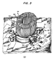
- FIG. 3 A perspective view of the electrical component surface mounted on a circuit substrate 300 (shown in fragmentary form) is shown in FIG. 3.
- the terminal members 317 and 318 connect the electrical device (inductor 350) of the component to the circuit conducting paths at the substrate.
- the tabs 311 and 312 represent the ends of one connecting conducting path and electrically connect the conducting leads 305 and 306.
- tabs 313 and 314 are the end at another connecting conducting path joining the conducting leads 307 and 308.
Landscapes
- Engineering & Computer Science (AREA)
- Manufacturing & Machinery (AREA)
- Microelectronics & Electronic Packaging (AREA)
- Power Engineering (AREA)
- Coils Or Transformers For Communication (AREA)
- Combinations Of Printed Boards (AREA)
- Coupling Device And Connection With Printed Circuit (AREA)
- Multi-Conductor Connections (AREA)
Claims (4)
- En combinaison :
un substrat de circuit (200; 300);
des premier (205; 305) et second (206; 306)
chemins conducteurs sur le substrat de circuit;
un composant électrique (250) prévu pour être monté sur le substrat, et comprenant :
un dispositif électrique (30);
un élément de base (10) destiné à supporter le dispositif électrique, comprenant :
des languettes (17, 18; 317; 318) qui sont destinées à recevoir des conducteurs de terminaisons (32-35) du dispositif électrique;
un chemin conducteur de connexion (20; 214) monté sur l'élément de base;
des première (11; 311) et seconde (12; 312) languettes supplémentaires auxquelles le chemin conducteur de connexion est connecté;
les première et seconde languettes supplémenres étant placées de façon à être connectées électriquement aux premier et second chemins conducteurs lorsque le composant électrique est monté sur le substrat de circuit. - La combinaison définie dans la revendication 1,
CARACTERISEE EN CE QUE
le chemin conducteur de connexion comprend un conducteur en cuivre plat qui est relié par un fil étamé (15) aux première et seconde languettes. - La combinaison définie dans la revendication 2,
CARACTERISEE EN OUTRE PAR
des troisième (209; 307) et quatrième (212; 308) chemins conducteurs sur le substrat de circuit,
un second chemin conducteur de connexion (21; 215) formé sur l'élément de base, et
des troisième (13; 313) et quatrième (14; 314) languettes supplémentaires, auxquelles le second chemin conducteur de connexion est connecté,
les troisième et quatrième languettes supplémentaires étant placées de façon à être connectées électriquement aux troisième et quatrième chemins conducteurs lorsque le composant électrique est monté sur le substrat de circuit. - Une combinaison définie dans la revendication 3,
CARACTERISEE EN CE QUE
le composant électrique est monté en surface sur le substrat.
Applications Claiming Priority (2)
| Application Number | Priority Date | Filing Date | Title |
|---|---|---|---|
| US06/900,558 US4754370A (en) | 1986-08-26 | 1986-08-26 | Electrical component with added connecting conducting paths |
| US900558 | 1997-07-25 |
Publications (3)
| Publication Number | Publication Date |
|---|---|
| EP0257738A2 EP0257738A2 (fr) | 1988-03-02 |
| EP0257738A3 EP0257738A3 (en) | 1989-12-06 |
| EP0257738B1 true EP0257738B1 (fr) | 1992-10-28 |
Family
ID=25412713
Family Applications (1)
| Application Number | Title | Priority Date | Filing Date |
|---|---|---|---|
| EP87305109A Expired EP0257738B1 (fr) | 1986-08-26 | 1987-06-10 | Composants électriques à pièces conductrices ajoutées |
Country Status (5)
| Country | Link |
|---|---|
| US (1) | US4754370A (fr) |
| EP (1) | EP0257738B1 (fr) |
| JP (1) | JPS6366868A (fr) |
| CA (1) | CA1257011A (fr) |
| DE (1) | DE3782380T2 (fr) |
Families Citing this family (13)
| Publication number | Priority date | Publication date | Assignee | Title |
|---|---|---|---|---|
| JPS63142894A (ja) * | 1986-12-06 | 1988-06-15 | 株式会社東芝 | フラツトパツケ−ジ集積回路の配線基板 |
| US5351167A (en) * | 1992-01-24 | 1994-09-27 | Pulse Engineering, Inc. | Self-leaded surface mounted rod inductor |
| US5212345A (en) * | 1992-01-24 | 1993-05-18 | Pulse Engineering, Inc. | Self leaded surface mounted coplanar header |
| GB2296387B (en) * | 1994-12-02 | 1999-10-13 | Dale Electronics | Low profile inductor/transformer component |
| US6102741A (en) * | 1996-06-03 | 2000-08-15 | Amphenol Corporation | Common mode filter connector with isolation |
| AT407463B (de) * | 1998-06-04 | 2001-03-26 | Siemens Ag Oesterreich | Spule zur stehenden montage auf schaltungsträgern |
| US6570478B2 (en) * | 2000-06-15 | 2003-05-27 | Standex Electronics | Surface mounted low profile inductor |
| DE10124378A1 (de) * | 2001-05-18 | 2002-11-21 | Pemetzrieder Neosid | Induktives Miniaturbauelement für SMD-Montage sowie Verfahren zu seiner Herstellung |
| US7002074B2 (en) | 2002-03-27 | 2006-02-21 | Tyco Electronics Corporation | Self-leaded surface mount component holder |
| US20030184423A1 (en) * | 2002-03-27 | 2003-10-02 | Holdahl Jimmy D. | Low profile high current multiple gap inductor assembly |
| US6897753B2 (en) | 2002-09-03 | 2005-05-24 | Artesyn Technologies, Inc. | Housing for a transformer |
| JP4317394B2 (ja) * | 2003-07-01 | 2009-08-19 | スミダコーポレーション株式会社 | 面実装インダクタ |
| US6986684B1 (en) * | 2004-11-10 | 2006-01-17 | Superworld Electronics Co., Ltd. | Internal structure for connector with coil positioning seats |
Family Cites Families (10)
| Publication number | Priority date | Publication date | Assignee | Title |
|---|---|---|---|---|
| US2927251A (en) * | 1955-04-28 | 1960-03-01 | Burroughs Corp | Arrangement and method for connecting electrical circuit elements |
| US3670208A (en) * | 1970-07-13 | 1972-06-13 | Logic Dynamics Inc | Microelectronic package, buss strip and printed circuit base assembly |
| US3959579A (en) * | 1974-08-19 | 1976-05-25 | International Business Machines Corporation | Apertured semi-conductor device mounted on a substrate |
| US4372037A (en) * | 1975-03-03 | 1983-02-08 | Hughes Aircraft Company | Large area hybrid microcircuit assembly |
| GB1501500A (en) * | 1975-06-20 | 1978-02-15 | Int Computers Ltd | Multilayer printed circuit boards |
| US4130722A (en) * | 1977-01-10 | 1978-12-19 | Globe-Union Inc. | Thick-film circuit module including a monolithic ceramic cross-over device |
| US4288841A (en) * | 1979-09-20 | 1981-09-08 | Bell Telephone Laboratories, Incorporated | Double cavity semiconductor chip carrier |
| US4591950A (en) * | 1983-09-09 | 1986-05-27 | American Manufacturing Company, Inc. | Circuit board-terminal-housing assembly |
| US4628411A (en) * | 1984-03-12 | 1986-12-09 | International Business Machines Corporation | Apparatus for directly powering a multi-chip module from a power distribution bus |
| JPS61151386U (fr) * | 1985-03-12 | 1986-09-18 |
-
1986
- 1986-08-26 US US06/900,558 patent/US4754370A/en not_active Expired - Fee Related
-
1987
- 1987-06-09 CA CA000539225A patent/CA1257011A/fr not_active Expired
- 1987-06-10 DE DE8787305109T patent/DE3782380T2/de not_active Expired - Fee Related
- 1987-06-10 EP EP87305109A patent/EP0257738B1/fr not_active Expired
- 1987-08-26 JP JP62210354A patent/JPS6366868A/ja active Pending
Also Published As
| Publication number | Publication date |
|---|---|
| DE3782380T2 (de) | 1993-03-11 |
| EP0257738A3 (en) | 1989-12-06 |
| EP0257738A2 (fr) | 1988-03-02 |
| JPS6366868A (ja) | 1988-03-25 |
| DE3782380D1 (de) | 1992-12-03 |
| US4754370A (en) | 1988-06-28 |
| CA1257011A (fr) | 1989-07-04 |
Similar Documents
| Publication | Publication Date | Title |
|---|---|---|
| US5386206A (en) | Layered transformer coil having conductors projecting into through holes | |
| US5251108A (en) | Laminated electronic device with staggered holes in the conductors | |
| EP0257738B1 (fr) | Composants électriques à pièces conductrices ajoutées | |
| JP2649491B2 (ja) | Smd構造の抵抗器、その製造方法及びこの抵抗器を取り付けたプリント回路板 | |
| US5321380A (en) | Low profile printed circuit board | |
| US5565837A (en) | Low profile printed circuit board | |
| US6903938B2 (en) | Printed circuit board | |
| US5363081A (en) | Line transformer and manufacturing process thereof | |
| US20050181684A1 (en) | Electronic component | |
| US5402098A (en) | Coil | |
| WO1999019934A1 (fr) | Dispositif de couplage pour montage en surface | |
| CN101502187A (zh) | 具有可构形的接地联接、共面的电路和接地轨迹的电路板 | |
| JPH0214794B2 (fr) | ||
| JPH03183106A (ja) | プリント配線板 | |
| US4136356A (en) | Wiring substrate for a matrix circuit | |
| US4652065A (en) | Method and apparatus for providing a carrier termination for a semiconductor package | |
| US5708568A (en) | Electronic module with low impedance ground connection using flexible circuits | |
| US4967175A (en) | Inductor and carrier suitable for attaching to a hybrid substrate or the like | |
| EP0287681A1 (fr) | Carte a circuits imprimes multi-couche et son procede de fabrication | |
| US6310536B1 (en) | Termination resistor in printed circuit board | |
| JPH07272934A (ja) | プリント基板 | |
| JPH05183274A (ja) | プリント回路基板 | |
| US4962287A (en) | Flexible printed wire board | |
| US5416274A (en) | Circuit board | |
| JP2000077218A (ja) | チップ形抵抗ネットワーク |
Legal Events
| Date | Code | Title | Description |
|---|---|---|---|
| PUAI | Public reference made under article 153(3) epc to a published international application that has entered the european phase |
Free format text: ORIGINAL CODE: 0009012 |
|
| AK | Designated contracting states |
Kind code of ref document: A2 Designated state(s): DE FR GB IT NL |
|
| PUAL | Search report despatched |
Free format text: ORIGINAL CODE: 0009013 |
|
| AK | Designated contracting states |
Kind code of ref document: A3 Designated state(s): DE FR GB IT NL |
|
| 17P | Request for examination filed |
Effective date: 19900515 |
|
| 17Q | First examination report despatched |
Effective date: 19911212 |
|
| GRAA | (expected) grant |
Free format text: ORIGINAL CODE: 0009210 |
|
| AK | Designated contracting states |
Kind code of ref document: B1 Designated state(s): DE FR GB IT NL |
|
| REF | Corresponds to: |
Ref document number: 3782380 Country of ref document: DE Date of ref document: 19921203 |
|
| ET | Fr: translation filed | ||
| ITF | It: translation for a ep patent filed | ||
| PLBE | No opposition filed within time limit |
Free format text: ORIGINAL CODE: 0009261 |
|
| STAA | Information on the status of an ep patent application or granted ep patent |
Free format text: STATUS: NO OPPOSITION FILED WITHIN TIME LIMIT |
|
| 26N | No opposition filed | ||
| PGFP | Annual fee paid to national office [announced via postgrant information from national office to epo] |
Ref country code: FR Payment date: 19980507 Year of fee payment: 12 |
|
| PGFP | Annual fee paid to national office [announced via postgrant information from national office to epo] |
Ref country code: GB Payment date: 19980515 Year of fee payment: 12 |
|
| PGFP | Annual fee paid to national office [announced via postgrant information from national office to epo] |
Ref country code: NL Payment date: 19980518 Year of fee payment: 12 |
|
| PGFP | Annual fee paid to national office [announced via postgrant information from national office to epo] |
Ref country code: DE Payment date: 19980630 Year of fee payment: 12 |
|
| PG25 | Lapsed in a contracting state [announced via postgrant information from national office to epo] |
Ref country code: GB Free format text: LAPSE BECAUSE OF NON-PAYMENT OF DUE FEES Effective date: 19990610 |
|
| PG25 | Lapsed in a contracting state [announced via postgrant information from national office to epo] |
Ref country code: FR Free format text: THE PATENT HAS BEEN ANNULLED BY A DECISION OF A NATIONAL AUTHORITY Effective date: 19990630 |
|
| PG25 | Lapsed in a contracting state [announced via postgrant information from national office to epo] |
Ref country code: NL Free format text: LAPSE BECAUSE OF NON-PAYMENT OF DUE FEES Effective date: 20000101 |
|
| GBPC | Gb: european patent ceased through non-payment of renewal fee |
Effective date: 19990610 |
|
| NLV4 | Nl: lapsed or anulled due to non-payment of the annual fee |
Effective date: 20000101 |
|
| PG25 | Lapsed in a contracting state [announced via postgrant information from national office to epo] |
Ref country code: DE Free format text: LAPSE BECAUSE OF NON-PAYMENT OF DUE FEES Effective date: 20000503 |
|
| REG | Reference to a national code |
Ref country code: FR Ref legal event code: ST |
|
| PG25 | Lapsed in a contracting state [announced via postgrant information from national office to epo] |
Ref country code: IT Free format text: LAPSE BECAUSE OF NON-PAYMENT OF DUE FEES Effective date: 20050610 |