EP0313452B1 - Procédé de dépot de siliciure de métal réfractaire pour la fabrication de circuits intégrés - Google Patents
Procédé de dépot de siliciure de métal réfractaire pour la fabrication de circuits intégrés Download PDFInfo
- Publication number
- EP0313452B1 EP0313452B1 EP88402620A EP88402620A EP0313452B1 EP 0313452 B1 EP0313452 B1 EP 0313452B1 EP 88402620 A EP88402620 A EP 88402620A EP 88402620 A EP88402620 A EP 88402620A EP 0313452 B1 EP0313452 B1 EP 0313452B1
- Authority
- EP
- European Patent Office
- Prior art keywords
- silicon
- process according
- deposition
- precursor
- refractory metal
- Prior art date
- Legal status (The legal status is an assumption and is not a legal conclusion. Google has not performed a legal analysis and makes no representation as to the accuracy of the status listed.)
- Expired - Lifetime
Links
Images


Classifications
-
- C—CHEMISTRY; METALLURGY
- C23—COATING METALLIC MATERIAL; COATING MATERIAL WITH METALLIC MATERIAL; CHEMICAL SURFACE TREATMENT; DIFFUSION TREATMENT OF METALLIC MATERIAL; COATING BY VACUUM EVAPORATION, BY SPUTTERING, BY ION IMPLANTATION OR BY CHEMICAL VAPOUR DEPOSITION, IN GENERAL; INHIBITING CORROSION OF METALLIC MATERIAL OR INCRUSTATION IN GENERAL
- C23C—COATING METALLIC MATERIAL; COATING MATERIAL WITH METALLIC MATERIAL; SURFACE TREATMENT OF METALLIC MATERIAL BY DIFFUSION INTO THE SURFACE, BY CHEMICAL CONVERSION OR SUBSTITUTION; COATING BY VACUUM EVAPORATION, BY SPUTTERING, BY ION IMPLANTATION OR BY CHEMICAL VAPOUR DEPOSITION, IN GENERAL
- C23C16/00—Chemical coating by decomposition of gaseous compounds, without leaving reaction products of surface material in the coating, i.e. chemical vapour deposition [CVD] processes
- C23C16/22—Chemical coating by decomposition of gaseous compounds, without leaving reaction products of surface material in the coating, i.e. chemical vapour deposition [CVD] processes characterised by the deposition of inorganic material, other than metallic material
- C23C16/30—Deposition of compounds, mixtures or solid solutions, e.g. borides, carbides, nitrides
- C23C16/42—Silicides
-
- H—ELECTRICITY
- H10—SEMICONDUCTOR DEVICES; ELECTRIC SOLID-STATE DEVICES NOT OTHERWISE PROVIDED FOR
- H10D—INORGANIC ELECTRIC SEMICONDUCTOR DEVICES
- H10D64/00—Electrodes of devices having potential barriers
- H10D64/01—Manufacture or treatment
- H10D64/011—Manufacture or treatment of electrodes ohmically coupled to a semiconductor
- H10D64/0111—Manufacture or treatment of electrodes ohmically coupled to a semiconductor to Group IV semiconductors
- H10D64/0112—Manufacture or treatment of electrodes ohmically coupled to a semiconductor to Group IV semiconductors using conductive layers comprising silicides
-
- H—ELECTRICITY
- H10—SEMICONDUCTOR DEVICES; ELECTRIC SOLID-STATE DEVICES NOT OTHERWISE PROVIDED FOR
- H10P—GENERIC PROCESSES OR APPARATUS FOR THE MANUFACTURE OR TREATMENT OF DEVICES COVERED BY CLASS H10
- H10P14/00—Formation of materials, e.g. in the shape of layers or pillars
- H10P14/40—Formation of materials, e.g. in the shape of layers or pillars of conductive or resistive materials
- H10P14/412—Deposition of metallic or metal-silicide materials
- H10P14/414—Deposition of metallic or metal-silicide materials of metal-silicide materials
Definitions
- the present invention relates to a method of depositing refractory metal silicide by the chemical vapor deposition technique for the manufacture of integrated circuits.
- the problem of depositing refractory metal silicides from essentially fluorinated precursors is solved according to the invention.
- the deposition method according to the invention is characterized in that the refractory metal precursor is mixed in gaseous form with silicon sub-fluorides just before deposition.
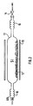
- FIG 1 appears a deposition oven comprising a sealed chamber 1, a vapor phase (CVD), provided with means 10 for depressurization not shown and gas analysis means (QMS), and a loading chamber 2 with a valve 9 make it possible to isolate the silicon wafers (Wafers) before loading and to avoid their contamination.
- a wafer 3 is placed in the sealed reaction chamber 1 on a support 4 comprising a halogen lamp 5, which makes it possible to heat the wafer 3 through a quartz plate 6.
- the precursor and vector gases are introduced above the section treated 3 by a nozzle 7.
- the temperatures are measured using an infrared thermometer 8.
- Figure 2 appears a tubular furnace for manufacturing sub-fluorides.
- the charge of SiF4 passes into the furnace 11 charged with pieces of silicon.
- the oven 11 is heated by electrical resistors capable of bringing the Si to approximately 1200 to 1500K.
- a valve 14 makes it possible to isolate the furnace 11 from the CVD device, (downstream of the valve 14).
- Hoses 15, 16 connect the furnace on the one hand to the source of SiF4 (not shown) and to the valve 14.
- the SiF2 and SiF3 species are generated by passing SiF4 over pieces of Si heated to 1400 K, as shown in FIG. 2. Under these temperature conditions, the mixture of fluoride and sub-fluorides comprises approximately 51% of SiF3, 46% of SiF4 and 3% of SiF2.
- This mixture of the precursors of W, WF6 and of silicon, the silicon sub-fluorides react according to the reaction: aWF6 + bSiF3 + cSiF2 ⁇ gWSi x + hSiF4 where a, b, c, g and h are thermodynamic parameters.
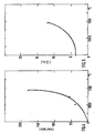
- Figure 3 shows that no deposit is made (thickness of the deposit (mm) as a function of the ratio of the WF6 / SF4 flow rates) when WF6 and SF4 are brought into contact, after a deposition period of 7 min and for a temperature 400 ° C silicon wafer.
- Figures 4 and 5 respectively represent the deposition speed (nm / min) and the resistivity of the deposition produced for various temperatures of the SiF4 furnace.
- the WF6 / SiF4 flow ratio is 1/50, the pressure of the order of 0.472-0.482 Torr, and the temperature of the wafer of 350 ° C.
- FIGS. 6 and 7 respectively represent the speed deposit and the resistivity of the deposited layer as a function of the ratio x of the H2 / SiF4 flow rates.
Landscapes
- Chemical & Material Sciences (AREA)
- Mechanical Engineering (AREA)
- Organic Chemistry (AREA)
- Chemical Kinetics & Catalysis (AREA)
- Engineering & Computer Science (AREA)
- Materials Engineering (AREA)
- Inorganic Chemistry (AREA)
- Metallurgy (AREA)
- General Chemical & Material Sciences (AREA)
- Chemical Vapour Deposition (AREA)
- Electrodes Of Semiconductors (AREA)
- Internal Circuitry In Semiconductor Integrated Circuit Devices (AREA)
- Silicon Compounds (AREA)
- Catalysts (AREA)
- Insulated Gate Type Field-Effect Transistor (AREA)
Description
- La présente invention concerne un procédé de dépôt de siliciure de métal réfractaire par la technique de dépôt chimique en phase vapeur pour la fabrication de circuits intégrés.
- Dans la fabrication de circuits intégrés, pour réaliser des interconnections en particulier, il est nécessaire de pouvoir déposer du silicium polycristallin, ou des métaux réfractaires, meilleurs conducteurs, ou encore des composés intermédiaires du type WSix, par exemple, c'est à dire des siliciures de métal réfractaire.
- Classiquement, on réalise la réaction:
WF₆ + 2 SiH₄→ WSi₂ + 6 HF + H₂
qui peut produire WSi₂ à partir de précurseurs classiques de W et du Si. Une telle réaction est par exemple décrite dans EP-A-0157052. D'une part, cette technique présente le désavantage de produire HF en grande quantité ce qui est néfaste tant pour les pompes que pour SiO₂. D'autre part, la demanderesse a mis en évidence que WF₆, en présence de SiF₄, peut ne donner aucun dépôt dans des conditions usuelles. - Le problème du dépôt de siliciures de métaux réfractaires à partir de précurseurs fluorés essentiellement est résolu selon l'invention. En effet, le procédé de dépôt selon l'invention est caractérisé en ce que le précurseur de métal réfractaire est mélangé sous forme gazeuse à des sous-fluorures de silicium juste avant le dépôt.
- Ce procédé permet des dépôts particulièrement non sélectifs et conformes. Les exemples et la description ci-dessous concernent des dépôts de WSix en particulier, mais d'autres métaux réfractaires sont cependant envisageables, comme Mo et Ti. Dans le cas du tungstène, selon l'invention, on utilise de préférence comme précursseur du WF₆.
- D'autre caractéristiques et avantages de l'invention apparaitront dans la description détaillée ci-après et sur les dessins annexés qui représentent:
- ― à la figure 1, un shéma de réacteur à parois froide en dépression pour la mise en oeuvre du procédé;
- ― à la figure 2, un shéma d'un four tubulaire pour produire des sous-fluorures;
- ― aux figures 3 à 7, des courbes présentant les résultats de dépôts réalisés comme cela sera décrit ci après.
- Sur la figure 1 apparait un four de dépôt comportant une chambre étanche 1, une phase vapeur (CVD), munis de moyens 10 de mise en dépression non représentés et de moyens d'analyse des gaz (QMS), et une chambre de chargement 2 avec une vanne 9 permettent d'isoler les tranches de silicium (Wafers) avant leur chargement et d'éviter leur contamination. Une tranche 3 est disposée dans la chambre de réaction étanche 1 sur un support 4 comportant une lampe à halogène 5, qui permet de chauffer la tranche 3 au travers d'une plaque de quartz 6. Les gaz précursseurs et vecteurs sont introduits au dessus de la tranche traitée 3 par une buse 7. Les températures sont mesurées à l'aide d'un thermomètre à infrarouge 8.
- A la figure 2 apparait un four tubulaire de fabrication des sous-fluorures.
- La charge de SiF₄ passe dans le four 11 chargé en morceaux de silicium. Le four 11 est chauffé par des résistances électriques capables de porter le Si à environ 1200 à 1500K. Une vanne 14 permet d'isoler le four 11 du dispositif de CVD, (en aval de la vanne 14). Des flexibles 15, 16 relient le four d'une part à la source de SiF₄ (non représentée) et à la vanne 14.
- Les espèces SiF₂ et SiF₃ sont générés par passage de SiF₄ sur des morceaux de Si chauffés à 1 400 K, comme le montre la figure 2. Dans ces conditions de température, le mélange de fluorure et sous-fluorures comporte environ 51% de SiF₃, 46% de SiF₄ et 3% de SiF₂.
- Ce mélange des précursseurs de W, WF₆ et de silicium, les sous-fluorures de silicium réagissent selon la réaction:
aWF₆ + bSiF₃ + cSiF₂ → gWSix + hSiF₄
où a, b, c, g et h sont des paramètres thermodynamiques. - La figure 3 montre qu'aucun dépôt n'est réalisé (épaisseur du dépôt (mm) en fonction du rapport des débits WF₆ / SF₄) quand on met en présence WF₆ et SF₄, après une durée de dépôt de 7 mn et pour une température de tranche de silicium de 400°C.
- Les figures 4 et 5 représentent respectivement la vitessse de dépôt (nm/min) et la résistivité du dépôt réalisé pour diverses températures du four à SiF₄. Le rapport de débit WF₆/SiF₄ est de 1/50, la pression de l'ordre de 0,472-0,482 Torr, et la température de la tranche de 350°C.
- Dans un mode de réalisation particulier, on peut mélanger aux précurseurs et gaz vecteurs classiquement utilisés (Ar et He) de l'hydrogène; un dépôt a lieu, pour une température de four à Si de 1090°C, une température de tranche de silicium de 350°C et une durée de dépôt de 5 mm, les figures 6 et 7 représentent respectivement la vitesse de dépôt et la résistivité de la couche déposée en fonction du rapport x des débits H₂/SiF₄.
Claims (8)
Priority Applications (1)
| Application Number | Priority Date | Filing Date | Title |
|---|---|---|---|
| AT88402620T ATE67629T1 (de) | 1987-10-19 | 1988-10-18 | Verfahren um hochschmelzendes metallsilizid niederzuschlagen zur herstellung von integrierten schaltungen. |
Applications Claiming Priority (2)
| Application Number | Priority Date | Filing Date | Title |
|---|---|---|---|
| FR8714383 | 1987-10-19 | ||
| FR8714383A FR2622052B1 (fr) | 1987-10-19 | 1987-10-19 | Procede de depot de siliciure de metal refractaire pour la fabrication de circuits integres |
Publications (2)
| Publication Number | Publication Date |
|---|---|
| EP0313452A1 EP0313452A1 (fr) | 1989-04-26 |
| EP0313452B1 true EP0313452B1 (fr) | 1991-09-18 |
Family
ID=9355934
Family Applications (1)
| Application Number | Title | Priority Date | Filing Date |
|---|---|---|---|
| EP88402620A Expired - Lifetime EP0313452B1 (fr) | 1987-10-19 | 1988-10-18 | Procédé de dépot de siliciure de métal réfractaire pour la fabrication de circuits intégrés |
Country Status (11)
| Country | Link |
|---|---|
| US (1) | US4981723A (fr) |
| EP (1) | EP0313452B1 (fr) |
| JP (1) | JPH027423A (fr) |
| KR (1) | KR890007388A (fr) |
| AT (1) | ATE67629T1 (fr) |
| CA (1) | CA1337547C (fr) |
| DE (1) | DE3864971D1 (fr) |
| ES (1) | ES2024672B3 (fr) |
| FI (1) | FI884788A7 (fr) |
| FR (1) | FR2622052B1 (fr) |
| NO (1) | NO884603L (fr) |
Families Citing this family (3)
| Publication number | Priority date | Publication date | Assignee | Title |
|---|---|---|---|---|
| KR930002673B1 (ko) * | 1990-07-05 | 1993-04-07 | 삼성전자 주식회사 | 고융점금속 성장방법 |
| TW396646B (en) | 1997-09-11 | 2000-07-01 | Lg Semicon Co Ltd | Manufacturing method of semiconductor devices |
| KR100425147B1 (ko) * | 1997-09-29 | 2004-05-17 | 주식회사 하이닉스반도체 | 반도체소자의제조방법 |
Family Cites Families (7)
| Publication number | Priority date | Publication date | Assignee | Title |
|---|---|---|---|---|
| JPS5860640A (ja) * | 1981-10-01 | 1983-04-11 | Hoya Corp | 光学ガラス |
| DE3141567C2 (de) * | 1981-10-20 | 1986-02-06 | Siemens AG, 1000 Berlin und 8000 München | Verfahren zum Herstellen von aus Tantal, Wolfram oder Molybdän bestehenden Schichten bei niedrigen Temperaturen und Verwendung dieser Schichten |
| US4557943A (en) * | 1983-10-31 | 1985-12-10 | Advanced Semiconductor Materials America, Inc. | Metal-silicide deposition using plasma-enhanced chemical vapor deposition |
| JPS60170234A (ja) * | 1984-02-15 | 1985-09-03 | Semiconductor Energy Lab Co Ltd | 気相反応装置および気相反応被膜作製方法 |
| US4629635A (en) * | 1984-03-16 | 1986-12-16 | Genus, Inc. | Process for depositing a low resistivity tungsten silicon composite film on a substrate |
| JPS61276976A (ja) * | 1985-05-31 | 1986-12-06 | Res Dev Corp Of Japan | 中間状態種を用いた熱cvd法によるシリコン含有高品質薄膜の製造方法及び装置 |
| US4684542A (en) * | 1986-08-11 | 1987-08-04 | International Business Machines Corporation | Low pressure chemical vapor deposition of tungsten silicide |
-
1987
- 1987-10-19 FR FR8714383A patent/FR2622052B1/fr not_active Expired - Fee Related
-
1988
- 1988-10-17 US US07/258,764 patent/US4981723A/en not_active Expired - Fee Related
- 1988-10-17 FI FI884788A patent/FI884788A7/fi not_active IP Right Cessation
- 1988-10-17 NO NO88884603A patent/NO884603L/no unknown
- 1988-10-18 EP EP88402620A patent/EP0313452B1/fr not_active Expired - Lifetime
- 1988-10-18 DE DE8888402620T patent/DE3864971D1/de not_active Expired - Lifetime
- 1988-10-18 KR KR1019880013562A patent/KR890007388A/ko not_active Withdrawn
- 1988-10-18 AT AT88402620T patent/ATE67629T1/de not_active IP Right Cessation
- 1988-10-18 ES ES88402620T patent/ES2024672B3/es not_active Expired - Lifetime
- 1988-10-18 JP JP63260693A patent/JPH027423A/ja active Pending
- 1988-10-18 CA CA000580443A patent/CA1337547C/fr not_active Expired - Fee Related
Non-Patent Citations (1)
| Title |
|---|
| JOURNAL OF MATERIALS SCIENCE, vol. 22, no. 2, février 1987, pages 547-553, Londres, GB; S.MOTOJIMA et al.: "PREPARATION AND PROPERTIES OF NICKEL SILICIDE LAYERS BY THE DIFFUSION AND CVD processes using Si2C16 as a source of silicon". * |
Also Published As
| Publication number | Publication date |
|---|---|
| DE3864971D1 (de) | 1991-10-24 |
| JPH027423A (ja) | 1990-01-11 |
| NO884603D0 (no) | 1988-10-17 |
| FR2622052B1 (fr) | 1990-02-16 |
| ATE67629T1 (de) | 1991-10-15 |
| NO884603L (no) | 1989-04-20 |
| EP0313452A1 (fr) | 1989-04-26 |
| US4981723A (en) | 1991-01-01 |
| FR2622052A1 (fr) | 1989-04-21 |
| FI884788L (fi) | 1989-04-20 |
| KR890007388A (ko) | 1989-06-19 |
| FI884788A7 (fi) | 1989-04-20 |
| ES2024672B3 (es) | 1992-03-01 |
| FI884788A0 (fi) | 1988-10-17 |
| CA1337547C (fr) | 1995-11-14 |
Similar Documents
| Publication | Publication Date | Title |
|---|---|---|
| KR100296533B1 (ko) | 실란의사용없이진공챔버내에서wf6환원에의해수행되는텅스텐cvd공정중에서의텅스텐핵형성방법 | |
| US6626188B2 (en) | Method for cleaning and preconditioning a chemical vapor deposition chamber dome | |
| US5421957A (en) | Low temperature etching in cold-wall CVD systems | |
| JP3902408B2 (ja) | セルフクリーニング用の遠隔プラズマソースを備えた半導体処理装置 | |
| KR100421572B1 (ko) | 화학적 기상 증착 챔버를 비활성화하는 방법 | |
| US4563367A (en) | Apparatus and method for high rate deposition and etching | |
| US5231056A (en) | Tungsten silicide (WSix) deposition process for semiconductor manufacture | |
| JP2004153265A (ja) | 酸化クリーニングガスを熱活性化する方法および装置 | |
| US20020185067A1 (en) | Apparatus and method for in-situ cleaning of a throttle valve in a CVD system | |
| US20070087579A1 (en) | Semiconductor device manufacturing method | |
| KR20040021533A (ko) | 반도체 기판에 막을 형성하는 방법 | |
| EP1619267A2 (fr) | Procédé pour enlever des résidus carbonnés d'un substrat | |
| JPH11162880A (ja) | 半導体装置の製造装置および半導体装置の製造方法 | |
| US5491112A (en) | Method and arrangement for treating silicon plates | |
| JP7414708B2 (ja) | 半導体膜を堆積させるための方法 | |
| EP0313452B1 (fr) | Procédé de dépot de siliciure de métal réfractaire pour la fabrication de circuits intégrés | |
| Kobayashi et al. | In situ infrared reflection and transmission absorption spectroscopy study of surface reactions in selective chemical‐vapor deposition of tungsten using WF6 and SiH4 | |
| EP1154036A1 (fr) | Réactions en phase gazeuse pour éliminer des contaminantes dans un réacteur CVD | |
| JPH0641631B2 (ja) | 酸化タンタル膜の化学気相成長法および化学気相成長装置 | |
| JPH11162875A (ja) | 半導体装置の製造方法 | |
| JPH1197434A (ja) | 成膜装置、クリーニング方法、及び成膜方法 | |
| JP2013541187A (ja) | 分子状フッ素を用いる化学気相成長チャンバのクリーニング | |
| JP3820212B2 (ja) | Cvdチャンバクリーニング後にcvdチャンバをコンディショニングする方法 | |
| KR930005947B1 (ko) | 반도체장치 제조방법 | |
| EP1154037A1 (fr) | Méthode pour améliorer un procédé de dépôt chimique en phase vapeur |
Legal Events
| Date | Code | Title | Description |
|---|---|---|---|
| PUAI | Public reference made under article 153(3) epc to a published international application that has entered the european phase |
Free format text: ORIGINAL CODE: 0009012 |
|
| 17P | Request for examination filed |
Effective date: 19881026 |
|
| AK | Designated contracting states |
Kind code of ref document: A1 Designated state(s): AT BE CH DE ES FR GB IT LI NL SE |
|
| 17Q | First examination report despatched |
Effective date: 19910305 |
|
| GRAA | (expected) grant |
Free format text: ORIGINAL CODE: 0009210 |
|
| AK | Designated contracting states |
Kind code of ref document: B1 Designated state(s): AT BE CH DE ES FR GB IT LI NL SE |
|
| ITF | It: translation for a ep patent filed | ||
| PG25 | Lapsed in a contracting state [announced via postgrant information from national office to epo] |
Ref country code: AT Effective date: 19910918 |
|
| REF | Corresponds to: |
Ref document number: 67629 Country of ref document: AT Date of ref document: 19911015 Kind code of ref document: T |
|
| REF | Corresponds to: |
Ref document number: 3864971 Country of ref document: DE Date of ref document: 19911024 |
|
| GBT | Gb: translation of ep patent filed (gb section 77(6)(a)/1977) | ||
| REG | Reference to a national code |
Ref country code: ES Ref legal event code: FG2A Ref document number: 2024672 Country of ref document: ES Kind code of ref document: B3 |
|
| PLBE | No opposition filed within time limit |
Free format text: ORIGINAL CODE: 0009261 |
|
| STAA | Information on the status of an ep patent application or granted ep patent |
Free format text: STATUS: NO OPPOSITION FILED WITHIN TIME LIMIT |
|
| 26N | No opposition filed | ||
| PGFP | Annual fee paid to national office [announced via postgrant information from national office to epo] |
Ref country code: CH Payment date: 19920915 Year of fee payment: 5 |
|
| PG25 | Lapsed in a contracting state [announced via postgrant information from national office to epo] |
Ref country code: LI Effective date: 19931031 Ref country code: CH Effective date: 19931031 |
|
| REG | Reference to a national code |
Ref country code: CH Ref legal event code: PL |
|
| EAL | Se: european patent in force in sweden |
Ref document number: 88402620.4 |
|
| PGFP | Annual fee paid to national office [announced via postgrant information from national office to epo] |
Ref country code: FR Payment date: 20000911 Year of fee payment: 13 |
|
| PGFP | Annual fee paid to national office [announced via postgrant information from national office to epo] |
Ref country code: GB Payment date: 20000919 Year of fee payment: 13 |
|
| PGFP | Annual fee paid to national office [announced via postgrant information from national office to epo] |
Ref country code: SE Payment date: 20000920 Year of fee payment: 13 |
|
| PGFP | Annual fee paid to national office [announced via postgrant information from national office to epo] |
Ref country code: NL Payment date: 20000925 Year of fee payment: 13 Ref country code: DE Payment date: 20000925 Year of fee payment: 13 |
|
| PGFP | Annual fee paid to national office [announced via postgrant information from national office to epo] |
Ref country code: ES Payment date: 20001009 Year of fee payment: 13 |
|
| PGFP | Annual fee paid to national office [announced via postgrant information from national office to epo] |
Ref country code: BE Payment date: 20001016 Year of fee payment: 13 |
|
| PG25 | Lapsed in a contracting state [announced via postgrant information from national office to epo] |
Ref country code: GB Free format text: LAPSE BECAUSE OF NON-PAYMENT OF DUE FEES Effective date: 20011018 |
|
| PG25 | Lapsed in a contracting state [announced via postgrant information from national office to epo] |
Ref country code: SE Free format text: LAPSE BECAUSE OF NON-PAYMENT OF DUE FEES Effective date: 20011019 Ref country code: ES Free format text: LAPSE BECAUSE OF NON-PAYMENT OF DUE FEES Effective date: 20011019 |
|
| PG25 | Lapsed in a contracting state [announced via postgrant information from national office to epo] |
Ref country code: BE Free format text: LAPSE BECAUSE OF NON-PAYMENT OF DUE FEES Effective date: 20011031 |
|
| REG | Reference to a national code |
Ref country code: GB Ref legal event code: IF02 |
|
| BERE | Be: lapsed |
Owner name: S.A. L' AIR LIQUIDE POUR L'ETUDE ET L'EXPLOITATION Effective date: 20011031 |
|
| PG25 | Lapsed in a contracting state [announced via postgrant information from national office to epo] |
Ref country code: NL Free format text: LAPSE BECAUSE OF NON-PAYMENT OF DUE FEES Effective date: 20020501 |
|
| EUG | Se: european patent has lapsed |
Ref document number: 88402620.4 |
|
| GBPC | Gb: european patent ceased through non-payment of renewal fee |
Effective date: 20011018 |
|
| PG25 | Lapsed in a contracting state [announced via postgrant information from national office to epo] |
Ref country code: FR Free format text: LAPSE BECAUSE OF NON-PAYMENT OF DUE FEES Effective date: 20020628 |
|
| NLV4 | Nl: lapsed or anulled due to non-payment of the annual fee |
Effective date: 20020501 |
|
| PG25 | Lapsed in a contracting state [announced via postgrant information from national office to epo] |
Ref country code: DE Free format text: LAPSE BECAUSE OF NON-PAYMENT OF DUE FEES Effective date: 20020702 |
|
| REG | Reference to a national code |
Ref country code: FR Ref legal event code: ST |
|
| REG | Reference to a national code |
Ref country code: ES Ref legal event code: FD2A Effective date: 20021113 |
|
| PG25 | Lapsed in a contracting state [announced via postgrant information from national office to epo] |
Ref country code: IT Free format text: LAPSE BECAUSE OF NON-PAYMENT OF DUE FEES;WARNING: LAPSES OF ITALIAN PATENTS WITH EFFECTIVE DATE BEFORE 2007 MAY HAVE OCCURRED AT ANY TIME BEFORE 2007. THE CORRECT EFFECTIVE DATE MAY BE DIFFERENT FROM THE ONE RECORDED. Effective date: 20051018 |