EP0334102B1 - Dispositif d'imprimante - Google Patents
Dispositif d'imprimante Download PDFInfo
- Publication number
- EP0334102B1 EP0334102B1 EP19890104025 EP89104025A EP0334102B1 EP 0334102 B1 EP0334102 B1 EP 0334102B1 EP 19890104025 EP19890104025 EP 19890104025 EP 89104025 A EP89104025 A EP 89104025A EP 0334102 B1 EP0334102 B1 EP 0334102B1
- Authority
- EP
- European Patent Office
- Prior art keywords
- block
- image memory
- data
- memory
- effective
- Prior art date
- Legal status (The legal status is an assumption and is not a legal conclusion. Google has not performed a legal analysis and makes no representation as to the accuracy of the status listed.)
- Expired - Lifetime
Links
Images


Classifications
-
- G—PHYSICS
- G06—COMPUTING OR CALCULATING; COUNTING
- G06T—IMAGE DATA PROCESSING OR GENERATION, IN GENERAL
- G06T1/00—General purpose image data processing
- G06T1/60—Memory management
-
- G—PHYSICS
- G06—COMPUTING OR CALCULATING; COUNTING
- G06K—GRAPHICAL DATA READING; PRESENTATION OF DATA; RECORD CARRIERS; HANDLING RECORD CARRIERS
- G06K15/00—Arrangements for producing a permanent visual presentation of the output data, e.g. computer output printers
-
- G—PHYSICS
- G06—COMPUTING OR CALCULATING; COUNTING
- G06K—GRAPHICAL DATA READING; PRESENTATION OF DATA; RECORD CARRIERS; HANDLING RECORD CARRIERS
- G06K2215/00—Arrangements for producing a permanent visual presentation of the output data
- G06K2215/0002—Handling the output data
- G06K2215/0062—Handling the output data combining generic and host data, e.g. filling a raster
- G06K2215/0065—Page or partial page composition
-
- G—PHYSICS
- G06—COMPUTING OR CALCULATING; COUNTING
- G06K—GRAPHICAL DATA READING; PRESENTATION OF DATA; RECORD CARRIERS; HANDLING RECORD CARRIERS
- G06K2215/00—Arrangements for producing a permanent visual presentation of the output data
- G06K2215/0002—Handling the output data
- G06K2215/0077—Raster outputting to the print element(s)
- G06K2215/008—Raster outputting to the print element(s) from more than one raster memory
Definitions
- the present invention relates to a printing apparatus for storing print data in an image memory and reading the print data for printing on printing paper.
- Known devices for printing on paper in accordance with print data generated by a host control unit include electrophotograph printers, thermal printers, wire-dot printers, and many others.
- the known printing apparatus comprises: a working memory for storing print data of virtual pages, an image memory for storing print data of effective blocks containing effective data, a printing section receiving the print data from the image memory for printing on the printing paper, an image memory control section for controlling writing of the print data in said image memory, and reading of the print data from the image memory, wherein said image memory control section comprises a block identifying section responsive to the print data from the working memory for each block to identify whether each block is an effective block containing effective data or an empty block containing no effective data, an address converting section for correlating the block addresses of the effective blocks within said virtual page with the block addresses within said image memory in which the data of said effective blocks are written by storing an address of the image memory block in which effective data of the virtual page block are stored, and storing mapping flags for indicating whether each block of the virtual page is an effective block or an empty block
- the prior art printing apparatus have limitations with respect to the operating speed or the memory size and the cost.
- An object of the invention is to improve the known printing apparatus with regard to memory space and processing time.
- Fig. 1 is a schematic diagram showing a printing apparatus according to the invention.
- Fig. 2 is a block diagram showing a print control unit.
- Fig. 3 is a schematic diagram showing the details of the image memory control section.
- Fig. 4 is a schematic diagram showing how the print data are output from the image memory in the prior art.
- Fig. 5 is a schematic diagram showing how the print data are stored in the image memory in the prior art.
- Fig. 6 is a schematic diagram showing how the print data are dismantled and assembled during writing into the image memory and during reading form the image memory.
- Fig. 7 is a schematic diagram showing details of the address converting section.
- Fig. 8 is a flow chart showing the operation of the printing apparatus during writing of the print data in the image memory.
- Fig. 9 is a flow chart showing the operating of the printing apparatus during reading of the print data from the image memory.
- Fig. 10 is a schematic diagram showing a modification of the address converting section.
- Fig. 11 is a schematic diagram showing another modification of the address converting section.
- Fig. 1 is a schematic view showing an electrophotograph printing apparatus, taken as an example for describing the invention.
- Fig. 2 is a block diagram showing a print control unit 8 which is incorporated in the printing apparatus of Fig. 1.
- Trays 11a and 11b contain sheets of printing paper 12 that are stacked. This printing paper 12 is picked up, one sheet at a time, by a hopping roller 13a or 13b and is made to travel along a transport path 14.
- a photosensitive drum 15 having a photosensitive layer on the periphery is disposed on the transport path 14.
- a writing device 16 writes electrostatic latent image on the outer periphery of the photosensitive drum 15.
- the photosensitive drum 15 is rotated in synchronism with the writing by the writing device 16.
- the writing device 16 is formed, for example, of a light-emitting diode array, a laser head, or the like.
- a light-emitting diodes array an array of light-emitting diodes "writes" an image onto the drum, one row of dots at a time.
- a beam of light "writes" the image onto the drum, while being scanned along the length of the drum.
- the image data or pixel signals to be written are supplied from an image memory 30 in the print control unit 8, shown in Fig. 2.
- a system bus 3 is connected via an interface 2 to a host control unit 1.
- a processor central processing unit, or CPU
- a program memory 5 is connected to the image memory control section 40.
- a font memory 7 is connected to the image memory control section 40.
- a print engine 10 which includes the writing device.
- the host control unit 1 is a device such as a computer, a word processor, or an image reading device, which generates print data.
- the interface 2 is a known circuit formed for example of a serial interface, such as the one identified by RS232C interface, or a parallel interface.
- the processor 4 performs control over the entire printing apparatus.
- the program for the operation of the processor 4 is stored in the program memory 5.
- the working memory 6 is formed of a random access memory, and stores and manages the data supplied through the interface 2.
- the font memory 7 converts character codes and other codes sent from the host control unit 1 into print font data, i.e., pixel signals representing the dots or pixels of print output.
- the image memory 30 is a random access memory for storing the print data that have been edited into the form of an image consisting of pixel signals.
- the image memory 30 has a capacity for image data or pixel signals making up one print output page, i.e., one complete page of printed paper.
- the image memory control section 40 controls writing in and reading from the image memory 30. It will later be described in further detail.
- the print engine 10 includes the writing device 16 shown in Fig. 1, and is responsive to the print data stored in the image memory 30 for printing on printing paper.
- the print engine interface 9 is an interface which follows the instructions from the processor 4 to read print data 9a from the image memory 30, to transfer the print data 9a to the print engine 10 or to accept print control signals 9b output from the print engine 10 and to transmit the control signals 9b to the processor 4 and other components.
- control commands, character codes, graphic commands, bit image data, and the like transmitted from the host control unit 1 via the interface 2 are stored in the working memory 6, and translated under control of the processor 4 into print data in the form of pixel signals and stored in the image memory 30.
- the image memory control section 40 will later be described in further detail.
- electrostatic latent image corresponding to the print data is created in succession.
- the latent image is developed by use of toner and transferred onto printing paper 12 and fixed. This printing process is effected continuously and cannot be interrupted. Accordingly, the transport of the printing paper is commenced after the print data is completely edited into the image memory 30.
- the printing paper 12 when the printing paper 12 is transported along the transport path 14 and reaches a transfer position Wo, the toner on the photosensitive drum 15 is transferred, and fixed by a fixing device, not shown, and the paper is then discharged.
- the transport of the printing paper 12 is interrupted at a point Wp on the transport path by a resist roller or the like, for standby, and resumed simultaneously with the writing of the latent image by the writing device 16. That is, while the photosensitive drum 15 rotates by l0 (angle ⁇ ), the printing paper 12 is transported by l0′ to reach the transfer position Wo.
- the print data are transferred from the image memory 30 in Fig. 2 to the writing device 16 when the hopping roller 13a has transported the printing paper 12 by l1, or the hopping roller 13b has transported the printing paper 12 by l1+l2.
- each virtual page contains 128 x 128 pixels, and one page consists of 8 rows x 10 columns of blocks.
- Blocks containing no effective data are regarded as an empty block, and the pixel signals for such an empty block are not stored in the image memory 30, but instead information indicating the emptiness is stored in a separated memory, to be described later, and a block of empty data (all "0") are supplied to the print engine 10 when the writing device 16 writes the image data on the drum 15.
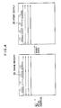
- Fig. 4 is a schematic diagram for explaining the reading operation of the print outputs from the image memory in the prior art.
- the image memory 30 is usually set to have a storage capacity adequate for print output 20 of one page.
- Fig. 4 shows allocation of words (each word containing 8 bits, for example) in the image memory schematically.
- the positions of the memory locations in the image memory correspond to the positions on the printing output page.
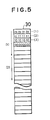
- Fig. 5 is another form of representation.
- the words are shown in an array, in a single sequence.
- the respective words of image data are stored in the respective memory locations in the image memory 30.
- each word of image data is stored in the image memory 30 corresponding to the position on the print output page at which the particular word of the image data should appear (i.e., should be printed). In the invention, this correspondence is not maintained. This is because words contained in the empty blocks are not stored in the image memory, and the effective blocks are stored in succession, without leaving empty blocks therebetween. This will be better understood from the following description of the concept of the invention with reference to Fig. 6.
- page [1] does not necessarily mean the first page in a series of pages making up of a complete document to be printed, but rather successive pages alternately named as page [1] and page [2].
- Each of the virtual pages is divided into blocks 62 and 62′.
- Each block may for example consists of 128 x 128 bits.
- the blocks can be classified into empty blocks 62′ containing empty data only (all "0"), and effective blocks 62 containing effective data (at least one bit having a value "1").
- the print control unit 8 shown in Fig. 2 writes only the data in the effective blocks 62 within the virtual pages in the image memory 30. With this arrangement, the image of the virtual pages are dismantled into segments, but the effective blocks 62 of more than one page can be concurrently stored in the image memory 30 having a capacity of a single print output page.
- print outputs corresponding to the virtual pages can be reproduced.
- the print data for the other virtual page can simultaneously be written in the image memory 30. Accordingly, when data of the first virtual page have been written in the image memory 30, they can be supplied to the writing device 16, and also writing of data of the second virtual page can be commenced. The data of the second virtual page can be written in the image memory 30 starting at the block next to the block in which the last effective block in the first virtual page is stored. Similarly, if data of a third virtual page are inputted, the effective blocks in the third virtual page can be written in the image memory 30, starting at the block next to the block in which the last effective block of the second virtual page is stored. Similar process is continued.
- the image memory 30 For rewriting the print data in the image memory 30, the image memory 30 has to be cleared before the writing new data. This is because of the algorithm used. In the invention, the clearance of the image memory is performed one block at a time, immediately before new data of an effective block are written. This contributes to a great saving of the memory clearance operation and the time therefor.
- Fig. 3 is a block diagram showing details of the image memory control section 40, and how its components are connected with other components in the printing apparatus shown in Fig. 1.
- the image memory control section 40 comprises a block identifying section 41 for receiving print data 60 from the working memory 6, dividing each virtual page consisting of image of one print output page, into a plurality of blocks, and identifying whether each block is an empty block consisting only of empty data or an effective block containing effective data.
- the image memory control section 40 also comprises a memory block assignment control section 42 for assigning a memory location in the image memory 30 for writing image data.
- the image memory control section 40 further comprises a block address generating section 43 for generating a block address, and a connection switching circuit 45 for switching the path for input of data to be written into the image memory 30 or for output of data read from the image memory 30.
- the memory block assignment control section 42, the block address generating section 43 and the connection switching section 45 form a writing control section which is responsive to the result of the identification by the block identifying section 41 for selecting only the effective blocks and for writing data into the image memory 30, block by block.
- the image memory control section 40 further comprises an address converting section 44 for performing address conversion. That is, the address converting section 44 correlates the virtual page block address, i.e., the block address within the virtual page with the image memory block address, i.e., the block address within the image memory 30 in which the effective block has been written, and storing mapping flags for discriminating between the effective block and the empty block within the virtual page, and a page identification flags for identifying the virtual page to which each effective block that has been written in the image memory belongs.
- the address converting section 44 correlates the virtual page block address, i.e., the block address within the virtual page with the image memory block address, i.e., the block address within the image memory 30 in which the effective block has been written, and storing mapping flags for discriminating between the effective block and the empty block within the virtual page, and a page identification flags for identifying the virtual page to which each effective block that has been written in the image memory belongs.
- the print data 60 for the virtual page 61 are divided into a plurality of blocks 62.
- Print data 60 in the working memory are processed page by page, and block by block.
- the block identifying section 41 judges whether each of the blocks 62 constituting the virtual page 61 is an empty block or an effective block. That is, the value of writing data, i.e., the number of bits having a value "1" in the word and a reference value 41a (data set for the level of the empty block, that is set at "0") are input to a comparator 41b provided in the block identifying section 41. When they match for all the words within a particular block, the block is found to be an empty block. When they do not match with regard to any of the words in the block, the block is found to be an effective block. The result of the identification is output to the block assignment control section 42.
- the memory block assignment control section 42 is a circuit formed of a microprocessor or the like for controlling writing of data into the image memory 30.
- the memory block assignment control section 42 is responsive to the result of identification output from the comparator 41b for performing control to prevent the writing of data into the image memory 30 when the block of the virtual page 61 consists of empty data only, and to permit writing of the data for inputting via the connection switching circuit 45 into the image memory 30 at proper memory locations when the block contains effective data.
- the address converting section 44 includes an address converting memory 44a and an empty block indication memory 44b.
- the address converting section 44 is illustrated in greater detail in Fig. 7.
- the address converting memory 44a stores, at each of the addresses corresponding to the block addresses Vn(x,y) of the respective virtual pages n, mapping flags T for indicating whether the particular block address of the virtual page is an effective block or an empty block, and in case of an effective block, the address RM(x,y) of the image memory block in which data of the virtual page block are stored.
- the address converting memory 44a has a capacity for storing flags for a plurality of virtual pages.
- the empty block indication memory 44b stores, at each of its memory locations corresponding to the image memory block addresses, page identification flags in columns P1 and P2 respectively corresponding to the virtual page [1] and the virtual page [2] for identifying the virtual page whose data have been written in each memory location in the image memory 30. That is, if the page identification flag is set at "1" in a column P1 at a certain address RM(x,y), it means that data of a block of the virtual page [1] are stored in the memory block RM(x,y) in the image memory 30.
- the page identifications flags are stored for all the image memory block addresses RM(x,y).
- the flags in the column P1 can be cleared and the column P1 can be used for storing the flags for a next virtual page, i.e., the third page, if the virtual page [1] and virtual page [2] initially correspond to the first and the second virtual pages.
- the fourth virtual page can use the column P2, and so on.
- the number of columns P1, P2 and the like can be increased. If for example, four columns P1 to P4 are provided, the first to fourth virtual pages can use the first to fourth columns P1 to P4, and the fifth virtual page is made use the first column P1, the sixth virtual page uses the second column P2, and so on.
- the memory block assignment control section 42 refers to the address converting section 44 for writing data of the virtual page, in the manner described with reference to Fig. 6, and reads the data via the connection switching circuit 45 to the print engine 10.
- Fig. 8 is a flow chart showing the operation of the data writing in the apparatus of the present invention.
- step S1 when writing operation is commenced, reading of the virtual page is conducted (step S1).
- the blocks are processed starting with the first block.
- step S2 judgment is made on whether or not the block read out is an empty block (step S2). In the case of the empty block, the flag T of the block of the corresponding page in the address converting memory is kept at "0" (step S3).
- step S4 judgment is made on whether or not the flag T is "1" (step S4). Initially, when the first data in the corresponding block is written, the flag T is at "0", so the flag T of the block of the corresponding virtual page in the address converting memory is set to "1" (step S5). Then, the empty block indication memory 44b is referred to, to determine the image memory block address RM(x,y) in which the data should be written (step S6).
- step S7 the corresponding block address RM(x,y) is written in the address converting memory 44a (step S7). Then, before the writing of the data, the corresponding image memory block is cleared (step S8). Then, the data in the effective block in the virtual page are written in the corresponding image memory block (step S9). After that, judgment is made on whether or not the writing operation for the entire virtual page has been completed (step S10). When the writing operation for the entire virtual page has not been completed, the next step is the step S1. After the first effective data in the block have been written the flag T is at "1", so the step S4 is followed by the step S9, and the next data are overwritten in the corresponding block in the image memory.
- step S4 is followed by the step S5.
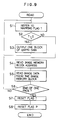
- Fig. 9 is a flow chart showing the operation of the data reading.
- step S1 the mapping flag T in the address converting memory is first referred to (step S1). Then, judgment is made on whether or not the flag T is "0" (step S2). If the flag T is at "0", the block in question is an empty block, so the empty data of one block is output (step S3). If the flag T is not at "0", the block in question is an effective block, then the corresponding image memory block at the address RM(x,y) is referred to (step S4). Then, the effective block of data at the image memory block address RM(x,y) are read out (step S5). After that, judgment is made on whether the reading for the one page has been completed (step S6). If it has not been completed, the next step is the step S1.
- step S7 the next step is the step S7.
- the flags T in the address converting memory 44a corresponding to the virtual page whose data have been read out are all reset.
- the flags in column P1 or P2 assigned to the particular virtual page are all reset (step S8).
- the image memory is not cleared.
- the page identification flag is set at "1", when the mapping has been made, and is set at "0" when the mapping has not been made. Accordingly, for each block of the image memory 30, the fact that the page identification flags are all"0" means that no mapping has been made on the block, and the fact that any of the page identification flags is at "1" mean that mapping has been made.
- the empty block indication memory 44b is referred to.
- the mapping flag is kept unchanged at "0" and the image memory block address RM(x,y) is kept indefinite.
- the memory block assignment control section 42 assigns an unused image memory block by referring to the page identification flags in the empty block indication memory 44b. For instance, the unused image memory block immediately following the series of the used image memory blocks is selected.
- the term "used image memory block” means the image memory block in which the image data waiting for printing are stored, while the term "unused image memory block” covers the image memory block from which the image data have already been read for being sent to the writing device 16 for printing, as well as the image memory block in which image data for printing have never been written after the system has started the operation.
- the appropriate page identification flag depending on which of the virtual page [1] and virtual page [2] is being written, is set at "1"
- the image memory block address RM(x,y) is written at the memory location Vn(x,y) in the address converting memory 44a corresponding to the virtual page block being written, and the mapping flag at the same memory location Vn(x,y) is set at "1”.
- the image memory block RM(x,y) which has been assigned to the virtual page block Vn(x,y) is cleared. After the memory clearance, the data of the particular virtual page block are written in the image memory block that has been assigned.
- the page identification flag is set in the column P1 in the empty block indication memory 44b to enable identification of the virtual page whose data have been stored in the memory block designated by the image memory block address RM(x,y).
- the address generating section 43 generates the virtual page addresses Vn(x,y) along the rasters in Fig. 3. Responsive to the addresses, the memory block assignment control section 42 refers to the mapping flag T at the address Vn(x,y) in the address converting memory 44a.
- mapping flag T at the address Vn(x,y) is at "1"
- the value of the image memory block address RM(x,y) as stored at the same address Vn(x,y) in the block address converting memory 44a is referred to and the data are read from the image memory block designated by the address value RM(x,y) as read out from the address converting memory 44a, and the print data are sent via the connection switching circuit 45 to the print engine 10.
- the mapping flag T which is referred to is at "0" the memory block assignment control section 42 generates empty data, which are then sent via the connection switching circuit 45 to the print engine 10, as the print data for the virtual page block.
- the image of the virtual page 61 can be reproduced as a print output, as shown in Fig. 6.
- the mapping flags T in the virtual page are all reset or cleared to "0". This permits the writing of the next virtual page.
- the block is found to be empty. If any of the words in the block is found to be effective, the block is found to be effective.
- mapping flag that is initially set at "0" is kept unchanged and the block address RM(x,y) in the image memory 30 is kept indefinite.
- the mapping flag T at the address Vn(x,y) in the address converting memory 44a is raised to "1”
- the address value RM(x,y) of the image memory block address is written at the memory location Vn(x,y)
- the page identification flag in the corresponding column P1 or P2, at the corresponding address is raised to "1".
- an unused image memory block RM(x,y) which has been assigned to the virtual page block Vn(x,y) is cleared, and then the data of the first word in the virtual page block are written in the appropriate, or corresponding word location in the image memory block that has been assigned. Following the data of the first word, data of the subsequent words in the same block are successively read. Each time reading is effected, when the mapping flag T is referred to, it is found to be set at "1" meaning that mapping has been made, so that the data are written in the corresponding word location in the image memory block.
- An address pointer is provided for the image memory 30 and incremented each time data of one word are written.
- the present invention is not limited to the above embodiments.
- the address converting section 44 can have different configurations. What are required of the address converting section 44 are that it correlates the virtual page block address with the image memory block address, that mapping flags are provided for identifying whether each virtual page block is an effective block or an empty block, and that page identification flags are provided for identifying the virtual page containing the effective block that has been written in each image memory block.
- Fig. 10 shows a modification of the address converting section.
- the address values are made to represent virtual page block addresses Vn(x,y) when the image memory block address RM(x,y) or the mapping flag T is referred to, while the address values are made to represent the image memory block addresses RM(x,y) when the page identification flags are referred to.
- each memory location can store 16 bits of information.
- the address converting section is configured assuming that the four virtual pages can be concurrently stored in the image memory. That is, four bits of page identification flags, one bit of the mapping flag, and remaining eleven bits of block addresses are provided.
- mapping flags T can be coded, mapping flags for four pages can be represented by two bits.
- Fig. 11 is another modification of the address converting section for the case where a larger number of virtual pages are written, i.e., more precisely, the sum of the number of virtual pages that can be stored concurrently in the image memory, and the number of bits of the addresses of the image memory block plus one for the mapping flag T is greater than the number of bits of the data that can be stored in each memory location (which is assumed to be 16).
- two adjacent memory locations are used in combination.
- page identification flags P1 to Px, and the mapping flag T and part of the image memory block address value RM(x,y) are stored.
- the remaining part of the image memory block address value RM(x,y) is stored.
- Each of the virtual page block addresses is made to correspond to the first memory location in each combination.
- the virtual page block addresses are made to correspond to the alternate memory locations.
- the structure of the address converting section 44 is simplified and the operation of the memory block assignment control section 42 can be simplified.
- the printing section is not limited to one of the electrophotography type, but can be of the wire dot type, and the like.
- the print control unit can be replaced by any of various circuits having similar functions.
- an image memory of a relatively small capacity such as one for a single page is used to store print data for two or more pages, and high-speed printing without waiting time is possible. Moreover, because of the reduction of the memory capacity, the cost of the printing apparatus can be lowered.
- clearance of the image memory is conducted for the parts corresponding to the effective blocks of the virtual page corresponding to the print data, so unnecessary clearance operation can be considerably reduced as compared with the prior art, with the result that the speed-up of the printing can be achieved.
Landscapes
- Engineering & Computer Science (AREA)
- Physics & Mathematics (AREA)
- General Physics & Mathematics (AREA)
- Theoretical Computer Science (AREA)
- General Engineering & Computer Science (AREA)
- Record Information Processing For Printing (AREA)
- Storing Facsimile Image Data (AREA)
Claims (7)
- Appareil d'impression pour imprimer sur un papier d'impression, page par page, dans lequel les données d'impression de chacune des pages virtuelles sont divisées en blocs, comprenant :
une mémoire de travail (6) pour stocker les données d'impression des pages virtuelles,
une mémoire d'image (30) pour stocker les données d'impression des blocs effectifs contenant les données effectives,
une section d'impression (10) recevant les données d'impression provenant de la mémoire d'image pour les imprimer sur le papier d'impression,
une section de commande de mémoire d'image (40) pour commander l'écriture des données d'impression dans ladite mémoire d'image (30), et pour commander la lecture des données d'impression provenant de la mémoire d'image (30),
dans lequel
ladite section de commande de mémoire d'image (40) comprend une section d'identification de bloc (41) sensible aux données d'impression provenant de la mémoire de travail (6) pour chaque bloc, pour identifier si chaque bloc est un bloc effectif contenant des données effectives ou un bloc vide ne contenant pas de données effectives,
une section de transformation d'adresse (44) sensible au résultat de l'identification de ladite section d'identification de bloc (41) pour corréler les adresses de bloc des blocs effectifs à l'intérieur de ladite page virtuelle aux adresses de bloc à l'intérieur de ladite mémoire d'image (30) dans laquelle les données desdits blocs effectifs sont écrites en stockant une adresse du bloc de mémoire d'image dans laquelle les données effectives du bloc de page virtuelle sont stockées, et pour stocker des indicateurs de cartographie (T) pour indiquer si chaque bloc de la page virtuelle est un bloc effectif ou un bloc vide, la section de transformation d'adresse comprenant, de plus, une mémoire d'indication de bloc vide (44b) qui stocke au niveau de chacun de ses emplacements de mémoire correspondant à ladite adresse de bloc de mémoire d'image, des indicateurs d'identification de page (P1, P2) pour identifier la page virtuelle à laquelle appartiennent les données de chaque bloc effectif qui ont été écrites dans ladite mémoire d'image, lesdits indicateurs d'identification de page étant agencés dans des colonnes respectives correspondant à la page virtuelle dont le bloc effectif est stocké dans ledit emplacement dans la mémoire d'image,
la section de commande d'attribution de bloc de mémoire (42) recevant le résultat de l'identification par ladite identification de bloc et se référant aux indicateurs d'identification de page, stockés dans ladite section de transformation d'adresse (44) pour attribuer, pendant l'écriture des données d'impression dans ladite mémoire d'image (30), un bloc dans la mémoire d'image qui est disponible pour les données d'impression d'un bloc effectif, l'attribution étant faite à la suite de sorte qu'aucun bloc vide n'est laissé entre des blocs effectifs,
ladite section de commande d'attribution de bloc de mémoire (42) commandant l'écriture des données d'impression des blocs effectifs dans ladite mémoire d'image (30) et pour éviter l'écriture des données dans ladite mémoire d'image lorsque le bloc est un bloc vide, et stockant les informations sur les données d'impression du bloc vide, et fournissant les données d'impression des blocs effectifs provenant de la mémoire d'image à la section d'impression (10) en se référant auxdits indicateurs d'identification de page, et fournissant les données d'impression des blocs vides à ladite section d'impression. - Appareil d'impression selon la revendication 1, dans lequel ladite section de commande de mémoire d'image (40) comprend, de plus, une section de production d'adresse de bloc (43) pour produire des adresses des données d'impression dans ladite mémoire de travail (6) pour fournir les données d'impression en provenance de la mémoire de travail (6), bloc par bloc, à ladite mémoire d'image (30).
- Appareil d'impression selon la revendication 2, dans lequel ladite section de production d'adresse (43) produit, de manière successive, des adresses de données pour chaque bloc, pendant l'écriture dans ladite mémoire d'image et pendant la lecture depuis ladite mémoire d'image.
- Appareil d'impression selon la revendication 1, dans lequel ladite section de commande d'attribution de bloc de mémoire (42) efface le bloc attribué dans ladite mémoire d'image (30) après l'attribution des données d'image et avant l'écriture des données d'impression dans ledit bloc.
- Appareil d'impression selon la revendication 1, dans lequel ladite section de commande de mémoire d'image (40) réinitialise ledit indicateur de cartographie et ledit indicateur d'identification de page après lecture des données du bloc effectif en provenance de ladite mémoire d'image.
- Appareil d'impression selon la revendication 1, dans lequel chacun desdits blocs est constitué de signaux d'éléments d'image correspondant à l'élément d'image disposé dans une zone rectangulaire dans la page de sortie d'impression.
- Appareil d'impression selon la revendication 1, dans lequel les données d'impression, telles que stockées dans ladite mémoire d'image et telles que fournies à ladite section d'impression, sont sous la forme de signaux d'éléments d'image représentant respectivement des points formant une matrice de points.
Applications Claiming Priority (4)
| Application Number | Priority Date | Filing Date | Title |
|---|---|---|---|
| JP63053555A JPH01228263A (ja) | 1988-03-09 | 1988-03-09 | 印刷装置 |
| JP53555/88 | 1988-03-09 | ||
| JP63146764A JPH023351A (ja) | 1988-06-16 | 1988-06-16 | 印刷装置 |
| JP146764/88 | 1988-06-16 |
Publications (2)
| Publication Number | Publication Date |
|---|---|
| EP0334102A1 EP0334102A1 (fr) | 1989-09-27 |
| EP0334102B1 true EP0334102B1 (fr) | 1994-11-30 |
Family
ID=26394269
Family Applications (1)
| Application Number | Title | Priority Date | Filing Date |
|---|---|---|---|
| EP19890104025 Expired - Lifetime EP0334102B1 (fr) | 1988-03-09 | 1989-03-07 | Dispositif d'imprimante |
Country Status (2)
| Country | Link |
|---|---|
| EP (1) | EP0334102B1 (fr) |
| DE (1) | DE68919493T2 (fr) |
Families Citing this family (2)
| Publication number | Priority date | Publication date | Assignee | Title |
|---|---|---|---|---|
| US5194899A (en) * | 1992-03-24 | 1993-03-16 | Lexmark International, Inc. | Complex page bit map composition |
| US5623585A (en) * | 1994-07-15 | 1997-04-22 | Eastman Kodak Company | Method and apparatus for parallel processing of a document image |
Family Cites Families (3)
| Publication number | Priority date | Publication date | Assignee | Title |
|---|---|---|---|---|
| US4074254A (en) * | 1976-07-22 | 1978-02-14 | International Business Machines Corporation | Xy addressable and updateable compressed video refresh buffer for digital tv display |
| JPS60181942A (ja) * | 1984-02-29 | 1985-09-17 | Fujitsu Ltd | メモリ制御装置 |
| ATE115749T1 (de) * | 1987-07-31 | 1994-12-15 | Qms Inc | Seitendrucksystem mit virtuellem speicher. |
-
1989
- 1989-03-07 EP EP19890104025 patent/EP0334102B1/fr not_active Expired - Lifetime
- 1989-03-07 DE DE1989619493 patent/DE68919493T2/de not_active Expired - Fee Related
Also Published As
| Publication number | Publication date |
|---|---|
| DE68919493D1 (de) | 1995-01-12 |
| EP0334102A1 (fr) | 1989-09-27 |
| DE68919493T2 (de) | 1995-06-22 |
Similar Documents
| Publication | Publication Date | Title |
|---|---|---|
| US4635212A (en) | Method for generating a rotated print pattern | |
| US5717840A (en) | Method and apparatus for printing according to a graphic language | |
| US5315691A (en) | Print control apparatus | |
| US5136688A (en) | Print data processing apparatus for an image forming apparatus | |
| US5237645A (en) | Printing apparatus | |
| EP0583101A2 (fr) | Méthode et appareil générateur de motif de caractères | |
| US6348975B1 (en) | Image processing apparatus, image processing method, and storage medium | |
| US5040129A (en) | Data processor for generating character image | |
| EP0458612B1 (fr) | Dispositif d'impression | |
| US6985260B1 (en) | Apparatus and method for drawing a gradient fill object | |
| EP0510931B1 (fr) | Procédé et appareil de sortie | |
| EP0334102B1 (fr) | Dispositif d'imprimante | |
| US5020004A (en) | Image output apparatus capable of outputting forms in special colors | |
| EP0554998B1 (fr) | Procédé et dispositif pour le traitement des images | |
| EP0481787B1 (fr) | Procédé et appareil de sortie | |
| US6061070A (en) | Character outputting | |
| EP0146714B1 (fr) | Méthode et dispositif de création d'affichages visuels de données d'un ensemble de données d'entrée | |
| JPH023351A (ja) | 印刷装置 | |
| US5781706A (en) | Reducing memory capacity requirements in image output while maintaining output speed | |
| EP0145888A2 (fr) | Méthode et dispositif de création d'affichages visuels de données d'un ensemble de données d'entrée | |
| JP2575227B2 (ja) | 印刷装置 | |
| JPH10304180A (ja) | 描画処理装置及び描画処理方法 | |
| JP2575208B2 (ja) | 印刷装置 | |
| JPH01228263A (ja) | 印刷装置 | |
| JPH02266965A (ja) | 印刷装置 |
Legal Events
| Date | Code | Title | Description |
|---|---|---|---|
| PUAI | Public reference made under article 153(3) epc to a published international application that has entered the european phase |
Free format text: ORIGINAL CODE: 0009012 |
|
| AK | Designated contracting states |
Kind code of ref document: A1 Designated state(s): DE FR GB |
|
| 17P | Request for examination filed |
Effective date: 19900327 |
|
| 17Q | First examination report despatched |
Effective date: 19921202 |
|
| GRAA | (expected) grant |
Free format text: ORIGINAL CODE: 0009210 |
|
| AK | Designated contracting states |
Kind code of ref document: B1 Designated state(s): DE FR GB |
|
| ET | Fr: translation filed | ||
| REF | Corresponds to: |
Ref document number: 68919493 Country of ref document: DE Date of ref document: 19950112 |
|
| PLBE | No opposition filed within time limit |
Free format text: ORIGINAL CODE: 0009261 |
|
| STAA | Information on the status of an ep patent application or granted ep patent |
Free format text: STATUS: NO OPPOSITION FILED WITHIN TIME LIMIT |
|
| 26N | No opposition filed | ||
| REG | Reference to a national code |
Ref country code: GB Ref legal event code: IF02 |
|
| PGFP | Annual fee paid to national office [announced via postgrant information from national office to epo] |
Ref country code: DE Payment date: 20070301 Year of fee payment: 19 |
|
| PGFP | Annual fee paid to national office [announced via postgrant information from national office to epo] |
Ref country code: GB Payment date: 20070307 Year of fee payment: 19 |
|
| PGFP | Annual fee paid to national office [announced via postgrant information from national office to epo] |
Ref country code: FR Payment date: 20070308 Year of fee payment: 19 |
|
| GBPC | Gb: european patent ceased through non-payment of renewal fee |
Effective date: 20080307 |
|
| REG | Reference to a national code |
Ref country code: FR Ref legal event code: ST Effective date: 20081125 |
|
| PG25 | Lapsed in a contracting state [announced via postgrant information from national office to epo] |
Ref country code: DE Free format text: LAPSE BECAUSE OF NON-PAYMENT OF DUE FEES Effective date: 20081001 |
|
| PG25 | Lapsed in a contracting state [announced via postgrant information from national office to epo] |
Ref country code: FR Free format text: LAPSE BECAUSE OF NON-PAYMENT OF DUE FEES Effective date: 20080331 |
|
| PG25 | Lapsed in a contracting state [announced via postgrant information from national office to epo] |
Ref country code: GB Free format text: LAPSE BECAUSE OF NON-PAYMENT OF DUE FEES Effective date: 20080307 |