EP0367536B1 - Rod base material for providing wafers used for electronic devices and a method of manufacturing wafers used for electronic device - Google Patents
Rod base material for providing wafers used for electronic devices and a method of manufacturing wafers used for electronic device Download PDFInfo
- Publication number
- EP0367536B1 EP0367536B1 EP89311180A EP89311180A EP0367536B1 EP 0367536 B1 EP0367536 B1 EP 0367536B1 EP 89311180 A EP89311180 A EP 89311180A EP 89311180 A EP89311180 A EP 89311180A EP 0367536 B1 EP0367536 B1 EP 0367536B1
- Authority
- EP
- European Patent Office
- Prior art keywords
- rod members
- wafer
- single crystal
- rod
- bonding
- Prior art date
- Legal status (The legal status is an assumption and is not a legal conclusion. Google has not performed a legal analysis and makes no representation as to the accuracy of the status listed.)
- Expired - Lifetime
Links
Images


Classifications
-
- H—ELECTRICITY
- H10—SEMICONDUCTOR DEVICES; ELECTRIC SOLID-STATE DEVICES NOT OTHERWISE PROVIDED FOR
- H10P—GENERIC PROCESSES OR APPARATUS FOR THE MANUFACTURE OR TREATMENT OF DEVICES COVERED BY CLASS H10
- H10P90/00—Preparation of wafers not covered by a single main group of this subclass, e.g. wafer reinforcement
-
- H—ELECTRICITY
- H10—SEMICONDUCTOR DEVICES; ELECTRIC SOLID-STATE DEVICES NOT OTHERWISE PROVIDED FOR
- H10P—GENERIC PROCESSES OR APPARATUS FOR THE MANUFACTURE OR TREATMENT OF DEVICES COVERED BY CLASS H10
- H10P52/00—Grinding, lapping or polishing of wafers, substrates or parts of devices
-
- C—CHEMISTRY; METALLURGY
- C30—CRYSTAL GROWTH
- C30B—SINGLE-CRYSTAL GROWTH; UNIDIRECTIONAL SOLIDIFICATION OF EUTECTIC MATERIAL OR UNIDIRECTIONAL DEMIXING OF EUTECTOID MATERIAL; REFINING BY ZONE-MELTING OF MATERIAL; PRODUCTION OF A HOMOGENEOUS POLYCRYSTALLINE MATERIAL WITH DEFINED STRUCTURE; SINGLE CRYSTALS OR HOMOGENEOUS POLYCRYSTALLINE MATERIAL WITH DEFINED STRUCTURE; AFTER-TREATMENT OF SINGLE CRYSTALS OR A HOMOGENEOUS POLYCRYSTALLINE MATERIAL WITH DEFINED STRUCTURE; APPARATUS THEREFOR
- C30B29/00—Single crystals or homogeneous polycrystalline material with defined structure characterised by the material or by their shape
- C30B29/02—Elements
- C30B29/06—Silicon
-
- C—CHEMISTRY; METALLURGY
- C30—CRYSTAL GROWTH
- C30B—SINGLE-CRYSTAL GROWTH; UNIDIRECTIONAL SOLIDIFICATION OF EUTECTIC MATERIAL OR UNIDIRECTIONAL DEMIXING OF EUTECTOID MATERIAL; REFINING BY ZONE-MELTING OF MATERIAL; PRODUCTION OF A HOMOGENEOUS POLYCRYSTALLINE MATERIAL WITH DEFINED STRUCTURE; SINGLE CRYSTALS OR HOMOGENEOUS POLYCRYSTALLINE MATERIAL WITH DEFINED STRUCTURE; AFTER-TREATMENT OF SINGLE CRYSTALS OR A HOMOGENEOUS POLYCRYSTALLINE MATERIAL WITH DEFINED STRUCTURE; APPARATUS THEREFOR
- C30B33/00—After-treatment of single crystals or homogeneous polycrystalline material with defined structure
-
- H—ELECTRICITY
- H10—SEMICONDUCTOR DEVICES; ELECTRIC SOLID-STATE DEVICES NOT OTHERWISE PROVIDED FOR
- H10P—GENERIC PROCESSES OR APPARATUS FOR THE MANUFACTURE OR TREATMENT OF DEVICES COVERED BY CLASS H10
- H10P10/00—Bonding of wafers, substrates or parts of devices
- H10P10/12—Bonding of semiconductor wafers or semiconductor substrates to semiconductor wafers or semiconductor substrates
- H10P10/128—Bonding of semiconductor wafers or semiconductor substrates to semiconductor wafers or semiconductor substrates by direct semiconductor to semiconductor bonding
-
- Y—GENERAL TAGGING OF NEW TECHNOLOGICAL DEVELOPMENTS; GENERAL TAGGING OF CROSS-SECTIONAL TECHNOLOGIES SPANNING OVER SEVERAL SECTIONS OF THE IPC; TECHNICAL SUBJECTS COVERED BY FORMER USPC CROSS-REFERENCE ART COLLECTIONS [XRACs] AND DIGESTS
- Y10—TECHNICAL SUBJECTS COVERED BY FORMER USPC
- Y10S—TECHNICAL SUBJECTS COVERED BY FORMER USPC CROSS-REFERENCE ART COLLECTIONS [XRACs] AND DIGESTS
- Y10S148/00—Metal treatment
- Y10S148/012—Bonding, e.g. electrostatic for strain gauges
-
- Y—GENERAL TAGGING OF NEW TECHNOLOGICAL DEVELOPMENTS; GENERAL TAGGING OF CROSS-SECTIONAL TECHNOLOGIES SPANNING OVER SEVERAL SECTIONS OF THE IPC; TECHNICAL SUBJECTS COVERED BY FORMER USPC CROSS-REFERENCE ART COLLECTIONS [XRACs] AND DIGESTS
- Y10—TECHNICAL SUBJECTS COVERED BY FORMER USPC
- Y10S—TECHNICAL SUBJECTS COVERED BY FORMER USPC CROSS-REFERENCE ART COLLECTIONS [XRACs] AND DIGESTS
- Y10S148/00—Metal treatment
- Y10S148/017—Clean surfaces
-
- Y—GENERAL TAGGING OF NEW TECHNOLOGICAL DEVELOPMENTS; GENERAL TAGGING OF CROSS-SECTIONAL TECHNOLOGIES SPANNING OVER SEVERAL SECTIONS OF THE IPC; TECHNICAL SUBJECTS COVERED BY FORMER USPC CROSS-REFERENCE ART COLLECTIONS [XRACs] AND DIGESTS
- Y10—TECHNICAL SUBJECTS COVERED BY FORMER USPC
- Y10T—TECHNICAL SUBJECTS COVERED BY FORMER US CLASSIFICATION
- Y10T156/00—Adhesive bonding and miscellaneous chemical manufacture
- Y10T156/10—Methods of surface bonding and/or assembly therefor
- Y10T156/1052—Methods of surface bonding and/or assembly therefor with cutting, punching, tearing or severing
Definitions
- the present invention relates to a wafer for producing electronic devices, a process for producing wafers for electronic devices, and a rod assembly for the production of wafers.
- a Si single crystal ingot 1 is prepared as shown in Fig. 31.
- the outer circumference of the Si single crystal ingot 1 is shaped into a regular cylindrical form. Further, the upper end and the lower end in the longitudinal direction of the Si single crystal ingot 1 are removed.
- a planar portion 3 extended in the longitudinal direction is formed to the Si single crystal rod member 2 shaped into the regular cylindrical form for indicating the direction of the crystallographic axis of the single crystals.
- the rod member 2 of Si single crystals is applied with slicing thereby providing a plurality of Si single crystal wafers 4 each of a thickness of several hundreds of micrometers.
- FIG. 33 A plurality of wafers 4 thus obtained are shown in Fig. 33.
- the main surface 5 of the wafer 4 is mirror-finished by means of lapping and polishing.
- Fig. 34 illustrating the plan view of the wafer 4, a plurality of semiconductor integrated circuits 6 are formed on the main surface 5 of the wafer 4 in the subsequent steps.
- Fig. 34 various advantages can be obtained by forming a plurality of semiconductor integrated circuits 6 on one wafer 4.
- individual electronic devices such as vacuum tubes, resistance elements and capacitance elements had to be manufactured, basically, one by one even if they are mass-produced mechanically.
- electronic circuits had to be constituted by individual operations mainly by means of soldering. For instance, operations for connecting copper wires by means of soldering, operations for connection individual devices to printed circuit boards by means of soldering, etc. were required respectively.
- the photolithography step is preceded and followed by various steps such as an epitaxial step for laminating crystals on a Si single crystal wafer, an ion implantation step for introducing impurities into the single crystal wafer, a diffusion step for diffusing impurities introduced into the wafer, an oxidation step of applying an oxidative treatment to a specific region for selectively introducing impurities into the wafer or protecting the bonded surface, a CVD step, a metallizing step for forming electrodes or wirings, etc. These steps are applied not individually to each of the circuits but on every single crystal wafers or pluralities of the single crystal wafers.
- the manufacturing cost per one identical circuit constitution can be reduced outstanding by simultaneously forming a plurality of identical semiconductor integrated circuits on one identical single crystal wafer.
- the number of identical semiconductor integrated circuits that can be formed at a same time on the wafer may be increased.
- the leading principle for miniaturizing the minimum line width in the photolithography technology from the value greater than 10 ⁇ m to the value of less than 1.0 ⁇ m mainly consists in removal of defects. That is, for miniaturizing the circuits, it has been conducted to remove dusts present in the production steps, ensure the pattern accuracy by ensuring the mechanical accuracy for mask alignment upon photolithography, or eliminate defects or unnecessary impurities present in crystals or thin films. Accordingly, in order to realize them, not only the softwares for the steps have to be changed but also change of hardwares such as introduction of production facilities of higher performance has been required. That is, much investment in equipment cost is necessary on every reduction of design rules. In this way, if the production cost per identical circuit construction is intended to be reduced by the miniaturization of the circuits, the production cost can not be reduced as expected because of much investment in equipment.
- circuit miniaturization is intended to attain by applying improvement to steric structures (three dimensional structures) rather than by miniaturizing the planar circuit constitution, this increases the number of production steps required per unit wafer such as addition of trenching steps or lamination steps.
- UV-ray have usually been employed in the level of the existent design rules.
- UV-rays bring about deflection or interference, such UV-rays can no more be used under the design rule at submicron level. Accordingly, use of radiation-rays will be necessitated as a light source for the mask alignment by photolithography.
- difficulty in the circuit production is increased as the present design rule (e.g. the minimum dimension permitted) is reduced.
- An extreme difficulty is expected for reducing the minimum line width in the photolithography from 1.0 ⁇ m level to 0.1 ⁇ m level, that is, to increase the area effect by 100 times.
- the design rule at a submicron level the reduction for the cost of semiconductor integrated circuits in accordance with the reduction in the chip area by the circuit miniaturization is saturated. That is, further miniaturization will be accomplished at a cost which will preclude further reduction in cost per chip.
- Increase in the wafer diameter is determined, at first, by the production technology for single crystal ingot.
- the maximum diameter is 150mm (6 inch) at present.
- the maximum diameter for Si single crystal wafers at a trial level is 250mm (10 inch).
- the leading principle for increasing the wafer diameter from 25mm (1 inch) level to 250mm (10 inch) level consists in the scale-up of the facilities and removal of defects. That is, for the production of single crystal ingots of larger diameter, a facility of greater scale corresponding to the size is inevitably necessary. Along with the increase in the diameter of single crystal ingots, defects caused by localized stresses, etc. are brought about.
- the maximum diameter of Si single crystal ingots at the trial level is limited within a level of 250mm (10 inch) because of the reasons as described above. Further, the increase in the diameter of the Si single crystal wafer have developed from 50mm (2 inch) level only by each step of 25-50mm (1-2 inch) because of the same reasons as described above.
- the foregoing difficulty in increased along with the increase in the ingot diameter. That is, an extreme difficulty is expected for increasing the maximum ingot diameter from the 250mm (10 inch) level to the 500mm (20 inch) level, that is, for increasing the area effect by four times.
- reduction of the cost for the semiconductor integrated circuits in compliance with the increase in the area of the single crystal wafer by the increase in the ingot diameter is saturated. That is, capital costs of producing large diameter crystals offset economics of producing more chips per wafer at larger wafer diameters.
- a process for producing wafers for electronic device production which wafers are able to withstand stresses imposed by wafer handling and wafer processing in the course of electronic device production, as defined in claim 1.
- Optional features in this process are set out in claims 2 to 16.
- a wafer for producing electronic devices which wafer is able to withstand stresses imposed by wafer handling and wafer processing in the course of electronic device production, as defined in claim 17.
- Optional features of this wafer are set out in claims 18 to 23.
- a rod assembly for the production of wafers as defined in claim 24.
- Optional features of this assembly are set out in claims 25 to 27.
- Embodiments of the present invention provide a rod base material used for wafers capable of remarkable reduction of the cost of semiconductor integrated circuits.
- Embodiments of the present invention provide wafers used for electronic devices having a considerably greater area as compared with that of conventional wafers.
- Embodiments of the present invention provide a method for producing wafers capable of remarkably reducing the cost for semiconductor integrated circuits.
- Embodiments of the present invention provide a method for producing wafers used for electronic devices having considerably greater area as compared with that of conventional wafers.
- the rod base material in accordance with embodiments of the present invention provides a plurality of wafers used for electronic devices by slicing, in which a plurality of rod members prepared from materials which constitute wafers used for electronic devices are assembled in parallel and connected with each other into an integrated body.
- the wafer used for electronic devices in accordance with embodiments of the present invention is obtained by applying slicing to the rod base material as described above.
- a plurality of rod members are prepared at first and a mirror-finished joining surface is formed to the outer surface for each of the rod members. Then, the joining surface for each of the rod members is cleaned by surface treatment using chemicals. Then, respective rod members are assembled in parallel and respective joining surfaces are brought into contact with each other to prepare a rod base material as an assembly of the respective rod members. Then, the rod base material is maintained in a heated atmosphere. Finally, wafers for electronic devices are obtained by applying slicing of the rod base material formed as an integrated body.
- the rod base material has a structure in which a plurality of rod members are assembled in parallel and connected with each other into an integrated body, the diameter of the integrated body of rod base material can be remarkably increased. Accordingly, the diameter of the wafers obtained by slicing the rod base material is also increased remarkably. Since the wafer diameter is increased remarkably, the cost per one electronic device on the wafer is also reduced remarkably.
- the diameter of the rod base material is increased correspondingly. It is technically impossible to obtain a rod base material of such a large diameter as obtained in accordance with embodiments of the present invention from one ingot or, if it is possible, only at a remarkable increase in the production cost.
- a rod base material 7 shown in Fig. 1 comprises four rod members 8 each of a square prism shape prepared from Si single crystals which are assembled in parallel and connected with each other.
- the rod base material 7 as an assembly of four rod members 8 is then placed in a high temperature atmosphere.
- respective rod members 8 are firmly bonded to each other and, as a result, the rod base material 7 exhibits an appearance as if it was a single rod cut out from one Si single crystal ingot as shown in Fig. 2.
- a plurality of Si single crystal wafers 9 used for a plurality of electronic devices can be obtained as shown in Fig. 3.
- the main surface 10 of the wafer 9 is mirror finished, on which a plurality of semiconductor integrated circuits 11 are formed as shown in Fig. 4.
- Fig. 5 shows a preferred sequence of production steps for forming semiconductor integrated circuits on the main surface of the Si single crystal wafer.
- the production steps for forming the semiconductor integrated circuits are to be explained mainly referring to Fig. 5.
- step S1 four Si single crystal ingots 12 as shown in Fig. 6 are prepared.
- Each of the Si single crystal ingots 12 is removed with the upper end and the lower end in the longitudinal direction and, further, applied with grinding for the outer circumferential portion thereof to be formed into a square prism rod member 8 (step S2).
- a square prism rod member 8 each of an identical size are prepared as shown in Fig. 7.
- the side 8a of the rod member 8 is selected so as to direct a specific direction in order to indicate the direction of crystallographic axis of Si single crystals.
- Each of the rod members 8 has four sides 8a, among which specific sides to be in contact with adjacent rod members are mirror-finished by lapping and polishing (step S3).
- the surface accuracy on the mirror-finished surface is such that the flatness is less than 10 ⁇ m and the surface roughness is less than 10 nm. The accuracy at such a level can easily be attained by the existent techniques.
- step S4 surface treatment by means of chemicals is applied to the sides, which are to be joined, of each of the rod members 8 shaped into the square prism form.
- the side of the rod member 8 is coarsely washed and then degreased by being immersed in heated trichloroethylene (step S4).
- step S5 the side of the rod member 8 is immersed in a heated concentrated sulfuric acid.
- Deposits adhered to the side member 8 are removed by oxidation by the oxidative effect of the concentrated sulfuric acid. Possible deposits are, four example, organic dusts, etc. or metal dusts, etc.
- step S6 Si atoms situated on the side of the rod member 8 are oxidized by the oxidative effect of nitric acid and, as a result, the side of the rod member 8 is rendered from instable and not uniformly oxidized state into a stable and uniformly oxidized state.
- step S7 After washing the side of the rod member 8 with water, the side is immersed in a diluted aqueous fluoric acid solution (step S7). Then, the outermost surface of Si oxide film layers formed on the side of the rod member 8 is removed by the etching effect of fluoric acid to the Si oxide film layers and, at the same time, unnecessary atoms present at the outermost surface of the side are also removed.
- the steps may be applied repeatedly as required. Particularly, for rendering the outermost surface on the side of the rod member 8 into oxidized state or hydroxidized state, surface treatment using a nitric solution or a hydrogen peroxide solution may be applied to the side of the rod member 8.
- each of the rod members 8 is washed with water and dried (step S8).
- Fig. 7 four square prism rod members 8 shown in Fig. 7 are assembled in parallel in a clean atmosphere at room temperature so that their respective bonding faces (sides) are brought into contact with each other (step S9).
- the rod base material 7 as an assembly of four rod members 8 is shown in Fig. 1. If the side for each of the rod members 8 finished into a mirror-face state is an ideal surface in view of atom arrangement, respective rod members 8 assembled in parallel and brought into contact with each other, theoretically, form a jointless structure of Si single crystals. However, in an actual state, the surface of the side 8a for each of the rod members 8 is different from the ideal state.
- the side 8a of the rod member 8 when the side 8a of the rod member 8 is observed under magnification, the side will somewhat waving and a plurality of irregularities will be formed thereon. Accordingly, when the sides 8a for the respective rod members 8 are brought into contact with each other, the portion of contact is not present over the entire surface of the side of the rod member 8 but is present only in a partial region in view of the atom arrangement.
- the cleaning treatment is applied in a clean atmosphere, for example, to the sides of the respective rod members 8 in contact with adjacent rod members 8, a great amount of deposits such as dust, etc. are deposited to the sides from a micro point of view. Presence of such deposits hinder the contact between each of atoms for the respective rod members 8.
- Si atoms are not ideally exposed on the side for each of the rod members 8, but the surface portion of the side is generally in an oxidized or hyrdroxidized state.
- the oxide or hydroxide layers do not constitute a single atom layer but are in the state in which a plurality of not aligned atoms are overlapped with each other. Further, moistures, etc. are absorbed to the layer. Such a state also hinders contact between each of the atoms in adjacent rod members 8.
- the surface state on the sides 8a for the respective rod members 8 to be brought into contact with each other is different from the ideal state.
- the side for each of the rod member 8 has such a specular finish (e.g. optical flatness) and cleanness as are obtainable by the existing technical level
- the sides for the respective rod members 8 are joined with a bonding strength at a level of 5 kg/cm2 with the effect of hydrogen bond, etc. when they are brought into contact under the normal atmosphere at a room temperature, to thereby obtain an integrated rod base material 7 comprising Si single crystals.
- the rod base material 7 as the assembly of each of the rod members 8 is heated in a nitrogen atmosphere at about 400°C for 30 min (step S10).
- adsorbed molecules, mainly, of moisture etc. present in the portion of contact between each of the rod members 8 are removed.
- the rod base material 7 is heated in a nitrogen atmosphere at about 600°C for 30 min (step S11).
- the sides of the respective rod members 8 are joined with each other by way of oxygen due to condensating reaction or joined with each other by direct atom bonding of Si atoms.
- the rod base material 7 is heated in a nitrogen atmosphere at 1,000°C for one hour (step S12).
- the reaction described above takes place more completely.
- the heating and cooling procedures for the rod base material 7 are, of course, applied gradually for avoiding undesired effects of stresses.
- the respective rod members 8 When the respective rod members 8 are assembled in parallel and brought into contact with each other under the normal atmosphere at a room temperature, the respective rod members 8 are joined with each other with a bonding strength at a level of 5 kg/cm2.
- the respective rod members 8 By heating the assembly comprising each of the rod members 8 in a nitrogen atmosphere in the subsequent step, the respective rod members 8 are joined with each other by means of atom bonding with the bonding strength at a level of 100 to 200 kg/cm2.
- the rod base material 7 as an integrated comprising Si single crystals is obtained.
- the value of the bonding strength of from 100 to 200 kg/cm2 is at the same level as the tensile strength of Si single crystals.
- the rod base material as the assemble comprising each of the rod member 8 is integrated in view of the atom arrangement. If the difference in the direction of crystallographic axes between the sides for the respective rod members 8 is within 1 degree, the rod base material 7 comprises single crystals integrated from a crystallographic point of view. The difference in the direction of the crystallographic axes can be easily retained within the level of 1 degree by the existent technique although "1 degree" is not critical.
- the rod base material 7 is sliced to obtain plurality of Si single crystal wafers 9 each of a thickness of several hundreds of micrometers (step S19). This corresponds to the state shown in Fig. 3.
- the main surface 10 of the Si single crystal wafer 9 is mirror-finished by means of lapping and polishing (step S14).
- a plurality of semiconductor integrated circuits 11 are formed on the main surface of the Si single crystal wafer 9 finished into a mirror face (step S15). The state is shown in Fig. 4.
- the atom arrangement on the surface takes a structure as shown in Fig. 8, when schematically illustrated in a 2-dimensional view.
- Fig. 8 when schematically illustrated in a 2-dimensional view.
- Si Si atoms
- - means single bond
- ".” means a radical or potential bond.
- the actual surface of Si single crystals does not form an ideal surface even if it is polished physically or chemically into a mirror-finished state. That is, the actual surface of the Si single crystals is covered with a natural oxide film layer comprising several atom layers and the thickness of the film layer is about several nanometers (several tens of angstroms).
- a natural oxide film layer comprising several atom layers and the thickness of the film layer is about several nanometers (several tens of angstroms).
- Such an atom arrangement has a structure as shown in Fig. 9 when schematically illustrated in a 2-dimensional view.
- the natural oxide film layer 13 has OH groups on the terminal ends of the Si structure, or it adsorbs water (H2O) by hydrogen bonding.
- the atom arrangement when schematically illustrated in a 2-dimensional view, has a structure shown in Fig. 10.
- the reference numeral 14 denotes hydroxy groups and the reference numeral 15 denotes absorbed water.
- “H” denotes hydrogen atom and "---" denotes hydrogen bond.
- the ratio that the terminal end forms OH group or the ratio that it adsorbs water (H2O) by means of hydrogen bond is, of course, effected by the temperature and the humidity under which the natural oxide film layer is formed.
- organic materials such as oils present on the outermost surface have to be removed.
- an organic solvent there can be mentioned, for example, chlorine type solvent such as trichlene, dimethyl ethane and carbon tetrachloride, fluorine type solvent such as freon, ketone or alcohol solvent such as acetone or methanol.
- the organic materials may be burned to remove by the oxidative effect of heated sulfuric acid.
- a method of applying slight etching to the surface of the Si single crystals by means of an aqueous fluoric acid (HF) solution, thereby removing the organic material such as oils deposited to the surface is also effective.
- the atom arrangement at the surface when schematically illustrated in a 2-dimensional view, has a structure as shown in Fig. 10 described above. Further, by treating with an aqueous solution of hydrofluoric acid (HF) and applying water washing, all of the ends in the atom arrangement at the surface portion are basically terminated with hydroxy groups (OH group).
- HF hydrofluoric acid
- the surface of the Si single crystals may be treated with an aqueous solution having oxidative effect such as sulfric acid (H2SO4), nitric acid (HNO3), hydrogen peroxide (H2O2), etc. followed by water washing.
- H2SO4 sulfric acid
- HNO3 nitric acid
- H2O2O2O2 hydrogen peroxide
- atom arrangement in the bonded state in which all of the ends in the atom structure are terminated with hydroxy groups (OH group) at the surface of the Si single crystals when schematically illustrated in a 2-dimensional view, takes a structure as shown in Fig. 15.
- the portion depicted by the reference numeral 16 represents the region for the bonded portion.
- atom arrangement in the bonded state in which dehydrating condensation is taken place between hydroxy groups (OH group) at the surface of the Si single crystals and water (H2O) is absorbed to that portion when schematically illustrated in a 2-dimensional view, takes a structure as shown in Fig. 16.
- the portion depicted by the reference numeral 17 is a region for the bonded portion.
- the two mirror-finished surfaces of the Si single crystals applied with degreasing and cleaning by means of an acid type solution and then washed with water and dried to have hydrophilic property can easily be bonded by merely bringing them into contact with each other. If the Si single crystals are stored for a long period of time in dry atmosphere or excessively heated to dry before contact, hydroxy groups (OH group) at the terminal in the atom arrangement on the surface cause dehydrating condensation. Accordingly, it is not preferred to store them for a long time in dry atmosphere or heat and dry them excessively before contact. In addition, if the Si single crystals are stored for a long time in a room, etc. before contact, oils, etc. in air re-adsorbed to the surface of the Si single crystals, which is not preferred.
- Si surfaces having hydrophilic surfaces When two Si surfaces having hydrophilic surfaces are brought into contact with each other, it is preferred that they are kept in a somewhat wet state, because if there is a gap between the portion of contact of two surfaces of the Si single crystals, the gap-forming portion is bonded by the effect of hydrogen bond of water (H2O) and because this can prevent the adsorption of oils, etc. to the surface of contact.
- H2O hydrogen bond of water
- Si surfaces are kept in water when two Si surfaces are brought into contact with each other.
- a weight may be applied in addition to the self weight of the rod member of the Si single crystal or a pressure may be applied by means of a clamping device, jig, etc.
- the value varies within a range from 0.5 to 5.0 kg/cm2. If the surface roughness of the mirror-face of the Si single crystals is near 20 nm, the tensile strength takes a value of about 0.5 kg/cm2. On the other hand, if the surface roughness for the mirror-face of the Si single crystals is from 5 to 10 nm, the value of the tensile strength is about from 3.0 to 5.0 kg/cm2.
- the surface roughness for the mirror-face of the Si single crystals can be sufficiently reduced to about 2 nm by the existent technical level. Accordingly, there is no problem for the surface roughness of the mirror-face.
- the reason why the tensile strength varies as described above is attributable to the fact that the bonding between hydroxy groups (OH group) to each other by means of the hydrogen bonding is not present over the entire surface of the Si single crystals. In other words, if the hydroxy groups (OH group) are bonded to each other by means of the hydrogen bond over the entire surface of the Si single crystals, it is considered that the tensile strength takes a value at a level of 5 kg/cm2.
- the tensile strength is increased.
- the tensile strength starts to increase abruptly at a temperature in excess of 200°C.
- a value of about 50 kg/cm2 is obtained.
- the tensile strength is saturated (e.g. exhibits a substantially constant value) within a range of the heat temperature from 400 to 800°C.
- the tensile strength starts to increase further abruptly. If the temperature strength is measured after heating the rod members of the Si single crystals bonded to each other in the nitrogen atmosphere within the temperature range from 1000°C to 1200°C, a value from 100 to 200 kg/cm2 is obtained. In this case, destruction of the boundary is caused in the bulk of the Si single crystals, and the value of the tensile strength of 100 to 200 kg/cm2 is at an identical level for the tensile strength of the Si single crystals. It is to be understood that it is possible to form an integrated body like as a single crystal. In the meanwhile, the tensile strength is sufficient to withstand the slicing force at the slicing process.
- the tensile strength starts to increase abruptly when the heating temperature exceeds 200°C, because hydroxy groups (OH group) starts to take place dehydrating condensation to each other on the surface of contact of the rod members of the Si single crystals. Namely, it is considered that the hydrogen bonding between the hydroxy groups (OH groups) to each other starts to change to the bonding of Si-O-Si.
- the tensile is saturated within the range of the heating temperature of from 400°C to 800°C, because there is a balance between the increase of the void due to water (H2O) formed by the dehydrating condensation and the increase in the Si-O-Si bonding.
- H2O water
- the tensile strength starts to increase further abruptly if the heating temperature exceeds 800°C, because the voids start to decrease and the effect of increasing the Si-O-Si bonding becomes predominant. It is considered that the value of the tensile strength is settled to 100-200 kg/cm2 when the heating temperature reaches 1000°C - 1200°C, because the dehydrating condensation is completed.
- the rod members of the Si single crystals bonded to each other at a room temperature are heated in a nitrogen atmosphere at a temperature from 1000°C to 1200°C for about 2 hours, substantially complete bonding can be obtained.
- the heating rate to the rod members of the Si single crystals bonded to each other is such that the rod members of the Si single crystals are at first maintained at a temperature from 200°C to 400°C for about 30 min to one hour and, thereafter, maintained at a temperature of 400°C to 800°C for about 30 min to one hour, in order to prevent abrupt occurrence of voids.
- a nitrogen atmosphere may be used in a case where the flatness at the mirror-surface of the Si single crystals is satisfactory, but it is desirable to mix oxygen into nitrogen or mix steam and oxygen into nitrogen for making more reliable bonding over the entire mirror-finished surface of the Si single crystal.
- a weight may be added in addition to the self-weight of the rod members of the Si single crystal, or a pressure may be applied by means of clamping jig, in order to prevent undesired effects caused by vibrations, etc.
- the flatness for the mirror-finished face of the rod members of the Si single crystals is less than 10 ⁇ m.
- the allowable deviation from flatness is different also depending on the heating atmosphere, the heating temperature conditions and the heating time.
- the tolerance of allowable flatness is not affected by the chemical treatment or an applying force.
- the gap may be filled with silane type organic material having terminals capable of condensating reaction in the atom arrangement. While the silane organic materials are bonded to each other by means of hydrogen bond at a room temperature, they are condensated by heating to introduce Si-O-Si bonding or Si-Si bond into the gap between the non-contact surfaces. In the case of filling the silane organic material, it is required to restrict the amount as low as possible so as not to give undesired effect on the direct mirror-finished contact surfaces.
- the atom arrangement upon introducing the silane type organic material when schematically illustrated in a 2-dimensional view, takes a structure, for example, as shown in Fig. 18. In the drawing, the portion depicted by the reference numeral 19 is a region for the bonded portion.
- the rod base material 7 comprises four rod members 8 assembled in parallel and connected with each other into an integrated body.
- the area of the wafer 9 obtained by slicing the rod base material 7 has an area four times as large as that of the wafer obtained by slicing one rod member 8.
- the diameter of the Si single crystal wafer has been determined depending on the diameter of the single crystal ingot. In view of the production technique for the single crystal ingot, the maximum diameter of the Si single crystal wafer is 150mm (6 inch) at the mass production level. On the other hand, the maximum diameter of the Si single crystal wafer is 250mm (10 inch) at the trial level.
- the wafers 9 are obtained by assembling the four rod members 8 formed from single crystal ingots into an integrated circuit body and then slicing the rod base material 7 as the integrated body therefrom, it is possible to obtain a wafer of such a great diameter as can not be produced so far. In addition, Si single crystal wafers of such great area can be obtained at a relatively reduced cost.
- the rod base material 7 of the Si single crystal having a great cross sectional area is sliced and, further, by way of the steps such as lapping and polishing, Si single crystal wafer 9 of a great area is prepared.
- These steps basically comprise a plurality of divided steps operated on every surfaces. Accordingly, when comparing the case of preparing a plurality of the Si single crystal wafers each of a small area and the case of preparing one Si single crystal of such a great area as having the identical area with that of the total area for the plurality of wafers, the cost per area is possibly reduced in the case of the Si single crystal wafer 9 of a large area, with the reason as described below.
- the embodiment of the present invention can provide remarkable reduction in the cost. From an overall point of view, reduction in the cost obtained by manufacturing wafers by fabricating the rod base material as an assembly of a plurality of rod members is predominant over the increase in the cost required for assembling plurality of rod members.
- the embodiment of the present invention can provide reduction in the cost.
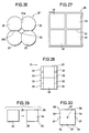
- the effect of the cost reduction becomes greater as the number of the assembled rod members 8 is increased (e.g. to 9, 16, 25 etc. or other numbers as shown in Figs. 21, 24 and 28).
- a plurality of semiconductor integrated circuits 11 are formed on the main surface 10 of the Si single crystal wafer 9. It is apparent that the number of the semiconductor integrated circuits to be formed on the wafer 9 is increased as the area of the wafer 9 is greater.
- a plurality of identical circuits can basically be manufactured by using photolithography technique. Accordingly, the production cost for one identical circuit constitution can be reduced outstandingly as compared with individual production of each one circuit. The effect of the cost reduction becomes increased as the number of the semiconductor integrated circuits 11 that are formed simultaneously is increased. Accordingly, the production cost per one identical circuit constitution is reduced as the area of the Si single crystal wafer 9 is greater.
- the Si single crystal wafer is processed on a single wafer or on a plurality of wafers at a time in the steps before and after the photolithography step. Accordingly, as the area of the Si single crystal wafer 9 is increased, more identical circuits can be manufactured at the same time, thereby enabling reduction of the production cost per one identical circuit constitution of the semiconductor integrated circuit.
- These steps can include, for example, an epitaxial step for making crystals grow on a Si single crystal wafer, an ion implantation step for introducing impurities into the single crystal wafer and a diffusing step subsequent thereto, an oxidizing step or CVD step for selectively introducing impurities or protecting the bonded surface, a metallizing step for forming electrodes or wiring layers, etc. These steps are applied on every single crystal wafers or on every lots of single crystal wafers.
- the cost per one semiconductor integrated circuit 11 can be reduced.
- the cost for semiconductor integrated circuit comprises design cost, material cost, fabrication cost, managing cost, etc.
- the design cost, the managing cost, etc. are relatively increased, they are generally utilizable, whereas the design cost, managing cost, etc. are relatively lower in the case of mass-produced products.
- the effect of reducing the fabrication cost in the embodiment of the present invention is particularly remarkable for the products having general utilizability and mass-produced, for example, main semiconductor integrated circuits such as memories of large capacity.
- the reason why the semiconductor integrated circuit industry is called a plant industry is that the production facilities are expensive. Particularly, facilities in the steps for wafer processing are expensive. Wafer processing steps at present will give an impression as if they are laboratories rather than factories, because the maximum diameter for the Si single crystal wafers that are put to practical use at present is at a level of 0.15 m and the area is too small to be used as the material for the mass-production in factories.
- the area of the Si single crystal wafer can be increased, theoretically, with no limit. For instance, it is possible to prepare a square-shaped Si single crystal wafer with 1.0 m length for one side.
- the rod members 8 are prepared by using Si single crystal ingots of the same size as those produced so far, and the rod members 8 are assembled in parallel to form a rod base material 7 which is then sliced to produce a Si single crystal wafer of a greater area, production facilities for the Si single crystal ingots used so far can be employed successively without discarding or obsolescence. That is, even when the increase in the area of the Si single crystal wafers has been progressed rapidly, production facilities used so far for the Si single crystal ingots are not wasted. Accordingly, increase in the area of the Si single wafers imposes not so large burden on Si wafer manufacturers.
- embodiments of the present invention may be applicable to other application uses. That is, if an embodiment of the present invention is applied to such a use that a plurality of electronic devices are formed simultaneously on a wafer, the cost for manufacturing the electronic devices will be reduced.
- individual semiconductor devices other than semiconductor integrated circuits there can be mentioned, for example, transistors, diodes, thyristors, etc. to which embodiments of the present invention are also applicable.
- embodiments of the present invention are also applicable to other electronic devices than the semiconductor devices, for example, resistance elements, and arrays, decoder, LED's and arrays, capacitance elements, sensors, etc.
- each of the rod members can be assembled to each other into an integrated body in the same method.
- rod members are connected with each other not by means of Si-O-Si bond but Ge-O-Ge bond.
- the melting point of Si is 1412°C
- the rod member of Si crystal can be heated to a temperature of 1200°C.
- the melting point of Ge is 958.5°C
- the heating temperature upon heating the Ge crystal rod member should not exceed 900°C.
- rod members comprising single crystals or polycrystals of compound semiconductors such as GaAs, InP and CdS, or to assemble and bond a plurality of rod members comprising oxides such as quartz (SiO2) or sapphire (Al2O3) with each other.
- oxides such as quartz (SiO2) or sapphire (Al2O3)
- the temperature is set as low as possible.
- SiO2 may be deposited intentionally on the rod member of the Si single crystal and, thereafter, Si single crystal rod member may be bonded to each other by means of SiO2.
- Various methods can be selected for depositing SiO2. For instance, the rod member of Si single crystals may be heated in a wet oxygen atmosphere (H2O + O2 + N2) at 900°C, thereby depositing oxide film layers of 0.5 - 2 ⁇ m thickness to the surface of the rod members.
- oxide film layers may be deposited to the surface of the rod members by using the thermal decomposing method of silane type compound (SiH4 + O2 or Si(OC2H5)4, etc.).
- oxide film layers of about 0.5 - 2 ⁇ m may be deposited to the surface of the rod member by a so-called CVD process.
- the chemical treatment and heat treatment after intentionally depositing SiO2 to the surface of the rod members of Si single crystal is the same as in the case of bonding the rod members of Si single crystals with each other.
- the rod members are more readily bonded with each other by intentionally depositing SiO2 to the surface of the rod members of Si single crystals, if the thickness of the oxide film layer is too great, it reduces the effect of compensating the gap at the surface of contact due to oxidation expansion of Si. Accordingly, excess increases in the thickness of the oxide film layers should be avoided.
- a plurality of rod members of Si single crystals may be bonded with each other by way of Si polycrystals.
- Si polycrystals can be deposited to the surface of the rod members of Si single crystals by means of thermal decomposition of silane (SiH4).
- SiH4 silane
- the deposited Si polycrystals provide an effect of moderating stresses.
- rod members comprising Ge crystals, rod members comprising various compound semiconductors, rod members comprising oxides, etc. can also be bonded with each other by way of materials different from that of such rod members.
- oxide film layers to the surface of rod members of GaAs single crystals by various methods.
- the rod members of GaAs single crystals are heated to a temperature from 350 to 500°C in a dry or wet atmosphere.
- the rod members of GaAs single crystals are oxidized at such a low temperature, for preventing dissociation.
- Oxides formed on the surface of the rod members of GaAs single crystals are Ga2O3.
- As2O3 can also be obtained as oxides.
- the surface of rod members of GaAs single crystals may be anodically oxidized by immersing them into an aqueous solution of NH4B5O8, an aqueous 1 % solution of HPO4, an aqueous 3 % solution of H3BO4, an aqueous 30 % of H2O2, etc.
- a plurality of rod members of GaAs single crystals may be bonded with each other by way of silicon nitride (Si3N4).
- silicon nitride (Si3N4) has an effect of preventing As dissociation under a high temperature.
- Si3N4 is deposited to the surface of the rod members of GaAs single crystals by means of CVD process (by thermal decomposition of SiH4 + NH3). Since there is no bonding force between each of Si3N4, polycrystalline Si is further deposited on the deposition layer of Si3N4 by means of CVD process (by way of thermal decomposition of SiH4). Then, SiO2 is deposited to the polycrystalline Si deposition layer by means of CVD process (by way of thermal decomposition of SiH4 + O2 or Si(C2H5)4). The subsequent chemical treatment and the heat treatment are the same as those for the rod members of Si single crystals described above. However, since the melting point of GaAs is 1238°C, it is desirable that the heating does not exceed 1000°.
- Al2O3 aluminum oxide
- Si3N4 silicon nitride
- CVD process by way of thermal decomposition of Al(OC3H7)3.
- Si polycrystals may directly be deposited to the surface of the rod members of GaAs single crystals, or SiO2 may be deposited directly if the flatness at the surface is satisfactory.
- a plurality of rod members comprising different material may be assembled in parallel and connected with each other into an integrated body.
- rod members comprising Si single crystals and rod members comprising GaAs single crystals may be deposited to the outermost surface of the rod members of GaAs single crystals.
- each of the rod members 8 to be assembled with each other has a square prism shape, it is not necessarily limited to such a shape.
- an ingot 19 is divided into one rod member 20 having a square cross sectional shape and four rod members 21 each having a trapezoidal cross sectional shape.
- rod members 21 and Fig. 22 it is also possible to assemble and connect a plurality of rod members 21 each having a trapezoidal cross sectional shape, after taken out from the ingot 19, with each other into one rod base material 22.
- the efficiency for utilizing material can be improved.
- an ingot 23 having a trapezoidal cross sectional shape as shown in Fig. 23.
- a GaAs ingot prepared by a Horizontal Bridgeman method forms a rod having a trapezoidal cross sectional shape as shown in Fig. 23.
- the rod members to be assembled is in a square prism shape. That is, the rod member has any configuration so long as it has a bonded face extended in the longitudinal direction thereof and finished into. a mirror-face state.
- a rod member 25 is substantially of a circular cylindrical shape having two bonded faces 25a, 25b.
- a cavity 26 is formed at the central portion thereof.
- the embodiment shown in Fig. 26 can increase the efficiency of using material and also provide a effect of moderating internal stresses caused at the inside of the rod base material 27.
- the 27 comprises Si single crystals, in which four square prism rod members 29 each having a square cross sectional shape are assembled and connected with each other into an integrated body.
- the respective rod members 29 are connected with each other by way of SiO2 film layers 30 intervening at the bonded faces.
- the material intervening between each of the rod members is not restricted only to the oxides of the rod member. For instance, nitrides or polycrystalline body of the rod member may be intervened. Otherwise, single crystals, polycrystals, oxides, nitrides, etc. of materials different from that of the rod member may be intervened.
- a rod base material 31 shown in Fig. 28 comprises rod members prepared from different material which are assembled in parallel and connected with each other into an integrated body.
- the rod base material 31 comprises two Si single crystal rod members 32 and eight GaAs single crystal members 33 which are assembled in parallel into an integrated body.
- each of the rod members 34 to be assembled is of a square prism shape, corners thereof may be chamfered as shown by the reference numeral 35.
- Fig. 30 shows a rod base material 36 comprising four such chamfered rod members 34 assembled in parallel into an integrated circuit body. Since the corners 35 of the rod member 34 are chamfered, recesses 37 and a cavity 38 are formed at the bonded portions for the respective rod members 34. In this embodiment, the bonded portion between each of the rod members can clearly observed. The cavity can help the water, which is produced by condensating reaction, to be away from the bonded portion.
- the rod base material providing a plurality of wafers for electronic devices by slicing comprises a plurality of rod members which are assembled in parallel and connected with each other into an integrated body, it is possible to obtain wafers used for electronic devices each having a considerably great area. Accordingly, wafers used for a lot of electronic devices can be formed on a wafer of a great area to reduce the cost per one electronic device.
Landscapes
- Chemical & Material Sciences (AREA)
- Engineering & Computer Science (AREA)
- Crystallography & Structural Chemistry (AREA)
- Materials Engineering (AREA)
- Metallurgy (AREA)
- Organic Chemistry (AREA)
- Crystals, And After-Treatments Of Crystals (AREA)
- Processing Of Stones Or Stones Resemblance Materials (AREA)
- Liquid Deposition Of Substances Of Which Semiconductor Devices Are Composed (AREA)
- Mechanical Treatment Of Semiconductor (AREA)
- Pressure Welding/Diffusion-Bonding (AREA)
Applications Claiming Priority (2)
| Application Number | Priority Date | Filing Date | Title |
|---|---|---|---|
| JP277975/88 | 1988-11-01 | ||
| JP63277975A JPH07101679B2 (ja) | 1988-11-01 | 1988-11-01 | 電子デバイス用ウエハ,ウエハ用棒状基材および電子デバイス |
Publications (3)
| Publication Number | Publication Date |
|---|---|
| EP0367536A2 EP0367536A2 (en) | 1990-05-09 |
| EP0367536A3 EP0367536A3 (en) | 1990-09-26 |
| EP0367536B1 true EP0367536B1 (en) | 1994-03-30 |
Family
ID=17590877
Family Applications (1)
| Application Number | Title | Priority Date | Filing Date |
|---|---|---|---|
| EP89311180A Expired - Lifetime EP0367536B1 (en) | 1988-11-01 | 1989-10-30 | Rod base material for providing wafers used for electronic devices and a method of manufacturing wafers used for electronic device |
Country Status (6)
| Country | Link |
|---|---|
| US (2) | US5105254A (ja) |
| EP (1) | EP0367536B1 (ja) |
| JP (1) | JPH07101679B2 (ja) |
| KR (1) | KR930010970B1 (ja) |
| CA (1) | CA2001934C (ja) |
| DE (1) | DE68914249T2 (ja) |
Cited By (1)
| Publication number | Priority date | Publication date | Assignee | Title |
|---|---|---|---|---|
| CN111452236A (zh) * | 2020-04-16 | 2020-07-28 | 西安奕斯伟硅片技术有限公司 | 晶棒粘接方法及晶棒粘接装置 |
Families Citing this family (22)
| Publication number | Priority date | Publication date | Assignee | Title |
|---|---|---|---|---|
| US5201977A (en) * | 1989-08-09 | 1993-04-13 | Hiroaki Aoshima | Process for producing structures from synthetic single-crystal pieces |
| JP2566175B2 (ja) * | 1990-04-27 | 1996-12-25 | セイコー電子工業株式会社 | 半導体装置及びその製造方法 |
| EP0456060B1 (en) * | 1990-04-27 | 1995-09-13 | Hiroaki Aoshima | Process for bonding synthetic singel crystals |
| JP2701709B2 (ja) * | 1993-02-16 | 1998-01-21 | 株式会社デンソー | 2つの材料の直接接合方法及び材料直接接合装置 |
| DE59309969D1 (de) * | 1993-05-28 | 2000-04-13 | Ibm | Verfahren zur Herstellung eines Plattenstapels aus direkt miteinander verbundenen Siliziumplatten |
| WO1996013060A1 (de) * | 1994-10-24 | 1996-05-02 | Daimler-Benz Aktiengesellschaft | Verfahren zum direkten verbinden von planaren körpern und nach dem verfahren aus planaren körpern hergestellte gegenstände |
| JPH0982588A (ja) * | 1995-09-12 | 1997-03-28 | Denso Corp | 窒化物の直接接合方法及びその直接接合物 |
| US6239038B1 (en) | 1995-10-13 | 2001-05-29 | Ziying Wen | Method for chemical processing semiconductor wafers |
| RU2160329C1 (ru) * | 1997-06-27 | 2000-12-10 | Ниппон Пиллар Пэкинг Ко., Лтд | МОНОКРИСТАЛЛ SiC И СПОСОБ ЕГО ПОЛУЧЕНИЯ |
| US5980873A (en) * | 1997-07-07 | 1999-11-09 | Kapral; Ales M. | Additive for cosmetics and other topically applied materials |
| KR100560853B1 (ko) * | 1997-10-06 | 2006-06-16 | 윤덕주 | 실리콘웨이퍼표면평활처리방법및장치 |
| US7637801B2 (en) | 2000-09-28 | 2009-12-29 | Sharp Kabushiki Kaisha | Method of making solar cell |
| JP3649393B2 (ja) * | 2000-09-28 | 2005-05-18 | シャープ株式会社 | シリコンウエハの加工方法、シリコンウエハおよびシリコンブロック |
| JP2002293686A (ja) * | 2001-04-03 | 2002-10-09 | Hitachi Cable Ltd | 化合物半導体単結晶の成長方法及びそれから切り出した基板 |
| DE102004010956B9 (de) * | 2004-03-03 | 2010-08-05 | Infineon Technologies Ag | Halbleiterbauteil mit einem dünnen Halbleiterchip und einem steifen Verdrahtungssubstrat sowie Verfahren zur Herstellung und Weiterverarbeitung von dünnen Halbleiterchips |
| JP4667263B2 (ja) * | 2006-02-02 | 2011-04-06 | シャープ株式会社 | シリコンウエハの製造方法 |
| JP4847836B2 (ja) * | 2006-09-29 | 2011-12-28 | 京セラキンセキ株式会社 | ウェハの製造方法 |
| JP5394043B2 (ja) * | 2007-11-19 | 2014-01-22 | 株式会社半導体エネルギー研究所 | 半導体基板及びそれを用いた半導体装置、並びにそれらの作製方法 |
| FR2939151A1 (fr) * | 2008-12-01 | 2010-06-04 | Soitec Silicon On Insulator | Lingots formes d'au moins deux lingots elementaires, un procede de fabrication et une plaquette qui en est issue |
| JP2011246315A (ja) * | 2010-05-28 | 2011-12-08 | Sumitomo Electric Ind Ltd | 炭化珪素基板およびその製造方法 |
| JP7149767B2 (ja) * | 2018-08-13 | 2022-10-07 | 昭和電工株式会社 | SiC単結晶の貼合方法、SiCインゴットの製造方法及びSiC単結晶成長用台座 |
| CN111270314A (zh) * | 2020-04-17 | 2020-06-12 | 中国电子科技南湖研究院 | 一种制备大尺寸单晶的方法 |
Family Cites Families (9)
| Publication number | Priority date | Publication date | Assignee | Title |
|---|---|---|---|---|
| US602159A (en) * | 1898-04-12 | Method of producing pyroxylin imitations of mosaic | ||
| US639015A (en) * | 1898-12-15 | 1899-12-12 | Edward G E Folkes | Feed-cutter. |
| US3235428A (en) * | 1963-04-10 | 1966-02-15 | Bell Telephone Labor Inc | Method of making integrated semiconductor devices |
| US3422527A (en) * | 1965-06-21 | 1969-01-21 | Int Rectifier Corp | Method of manufacture of high voltage solar cell |
| JPS56105638A (en) * | 1980-01-26 | 1981-08-22 | Sumitomo Electric Ind Ltd | Manufacture of circular gallium arsenide wafer |
| US4411731A (en) * | 1982-12-27 | 1983-10-25 | Bell Telephone Laboratories, Incorporated | Method of contouring crystal plates |
| JPS6051700A (ja) * | 1983-08-31 | 1985-03-23 | Toshiba Corp | シリコン結晶体の接合方法 |
| JPS6088536U (ja) * | 1983-11-24 | 1985-06-18 | 住友電気工業株式会社 | 化合物半導体ウエハ |
| JPS60227423A (ja) * | 1984-04-26 | 1985-11-12 | Fujitsu Ltd | インゴツトの接着方法 |
-
1988
- 1988-11-01 JP JP63277975A patent/JPH07101679B2/ja not_active Expired - Lifetime
-
1989
- 1989-10-30 DE DE68914249T patent/DE68914249T2/de not_active Expired - Fee Related
- 1989-10-30 EP EP89311180A patent/EP0367536B1/en not_active Expired - Lifetime
- 1989-10-30 US US07/427,887 patent/US5105254A/en not_active Expired - Fee Related
- 1989-10-31 CA CA002001934A patent/CA2001934C/en not_active Expired - Fee Related
- 1989-10-31 KR KR1019890015753A patent/KR930010970B1/ko not_active Expired - Fee Related
-
1991
- 1991-01-31 US US07/648,110 patent/US5100839A/en not_active Expired - Fee Related
Cited By (2)
| Publication number | Priority date | Publication date | Assignee | Title |
|---|---|---|---|---|
| CN111452236A (zh) * | 2020-04-16 | 2020-07-28 | 西安奕斯伟硅片技术有限公司 | 晶棒粘接方法及晶棒粘接装置 |
| CN111452236B (zh) * | 2020-04-16 | 2022-05-03 | 西安奕斯伟材料科技有限公司 | 晶棒粘接方法及晶棒粘接装置 |
Also Published As
| Publication number | Publication date |
|---|---|
| US5105254A (en) | 1992-04-14 |
| EP0367536A2 (en) | 1990-05-09 |
| CA2001934A1 (en) | 1990-05-01 |
| DE68914249T2 (de) | 1994-08-11 |
| KR930010970B1 (ko) | 1993-11-18 |
| KR900008619A (ko) | 1990-06-04 |
| EP0367536A3 (en) | 1990-09-26 |
| JPH02122617A (ja) | 1990-05-10 |
| CA2001934C (en) | 1994-10-18 |
| US5100839A (en) | 1992-03-31 |
| JPH07101679B2 (ja) | 1995-11-01 |
| DE68914249D1 (de) | 1994-05-05 |
Similar Documents
| Publication | Publication Date | Title |
|---|---|---|
| EP0367536B1 (en) | Rod base material for providing wafers used for electronic devices and a method of manufacturing wafers used for electronic device | |
| EP0854500B1 (en) | Method of manufacturing a bonded substrate | |
| JPH06252015A (ja) | 基板はり合わせ方法 | |
| US5918139A (en) | Method of manufacturing a bonding substrate | |
| JPH0963912A (ja) | 貼り合わせ基板製造方法 | |
| US5244830A (en) | Method for manufacturing a semiconductor substrate having a compound semiconductor layer on a single-crystal silicon wafer | |
| JPH0888272A (ja) | 半導体集積回路用基板の製造方法 | |
| JPS62283655A (ja) | 半導体多層基板の製造方法 | |
| KR940010159B1 (ko) | 반도체 기판의 제조 방법 | |
| RU2830141C1 (ru) | Способ соединения кремниевых пластин | |
| JP3668033B2 (ja) | シリコンウエハーの処理方法 | |
| JPH04199632A (ja) | Soiウエハ及びその製造方法 | |
| JPH01305534A (ja) | 半導体基板の製造方法 | |
| KR0171067B1 (ko) | 단결정 soi웨이퍼 제조방법 | |
| JP3099446B2 (ja) | 誘電体分離領域を有する半導体基板 | |
| JP4977938B2 (ja) | 3次元構造体の製造方法 | |
| KR0180622B1 (ko) | 저온에서의 실리콘 웨이퍼 접합에 의한 다층 구조의 soi 웨이퍼 제조 방법 및 이 방법에 의해 제조되는 soi 웨이퍼 | |
| JPH07169830A (ja) | 誘電体分離基板の製造方法 | |
| JPH02237066A (ja) | 半導体装置の製造方法 | |
| KR940005704B1 (ko) | 규소기판 직접 접착방법을 이용한 규소박막 제조방법 | |
| JPH03108356A (ja) | 半導体基板の製造方法 | |
| JP2581531B2 (ja) | 半導体装置の製造方法 | |
| JP3767794B2 (ja) | シリコンボートおよびその製造方法 | |
| KR100248358B1 (ko) | 접합형 soi 기판의 제조 방법 | |
| JPH0646622B2 (ja) | 半導体基板用シリコンウェハの製造方法 |
Legal Events
| Date | Code | Title | Description |
|---|---|---|---|
| PUAI | Public reference made under article 153(3) epc to a published international application that has entered the european phase |
Free format text: ORIGINAL CODE: 0009012 |
|
| AK | Designated contracting states |
Kind code of ref document: A2 Designated state(s): DE FR GB |
|
| PUAL | Search report despatched |
Free format text: ORIGINAL CODE: 0009013 |
|
| AK | Designated contracting states |
Kind code of ref document: A3 Designated state(s): DE FR GB |
|
| 17P | Request for examination filed |
Effective date: 19901217 |
|
| 17Q | First examination report despatched |
Effective date: 19920408 |
|
| GRAA | (expected) grant |
Free format text: ORIGINAL CODE: 0009210 |
|
| AK | Designated contracting states |
Kind code of ref document: B1 Designated state(s): DE FR GB |
|
| REF | Corresponds to: |
Ref document number: 68914249 Country of ref document: DE Date of ref document: 19940505 |
|
| ET | Fr: translation filed | ||
| PLBE | No opposition filed within time limit |
Free format text: ORIGINAL CODE: 0009261 |
|
| STAA | Information on the status of an ep patent application or granted ep patent |
Free format text: STATUS: NO OPPOSITION FILED WITHIN TIME LIMIT |
|
| 26N | No opposition filed | ||
| REG | Reference to a national code |
Ref country code: GB Ref legal event code: 746 Effective date: 19951106 |
|
| REG | Reference to a national code |
Ref country code: FR Ref legal event code: D6 |
|
| PGFP | Annual fee paid to national office [announced via postgrant information from national office to epo] |
Ref country code: FR Payment date: 19991011 Year of fee payment: 11 |
|
| PGFP | Annual fee paid to national office [announced via postgrant information from national office to epo] |
Ref country code: GB Payment date: 19991027 Year of fee payment: 11 |
|
| PGFP | Annual fee paid to national office [announced via postgrant information from national office to epo] |
Ref country code: DE Payment date: 19991102 Year of fee payment: 11 |
|
| PG25 | Lapsed in a contracting state [announced via postgrant information from national office to epo] |
Ref country code: GB Free format text: LAPSE BECAUSE OF NON-PAYMENT OF DUE FEES Effective date: 20001030 |
|
| GBPC | Gb: european patent ceased through non-payment of renewal fee |
Effective date: 20001030 |
|
| PG25 | Lapsed in a contracting state [announced via postgrant information from national office to epo] |
Ref country code: FR Free format text: LAPSE BECAUSE OF NON-PAYMENT OF DUE FEES Effective date: 20010629 |
|
| PG25 | Lapsed in a contracting state [announced via postgrant information from national office to epo] |
Ref country code: DE Free format text: LAPSE BECAUSE OF NON-PAYMENT OF DUE FEES Effective date: 20010703 |
|
| REG | Reference to a national code |
Ref country code: FR Ref legal event code: ST |