EP0381159B1 - Dispositif générateur de son musical - Google Patents
Dispositif générateur de son musical Download PDFInfo
- Publication number
- EP0381159B1 EP0381159B1 EP90101837A EP90101837A EP0381159B1 EP 0381159 B1 EP0381159 B1 EP 0381159B1 EP 90101837 A EP90101837 A EP 90101837A EP 90101837 A EP90101837 A EP 90101837A EP 0381159 B1 EP0381159 B1 EP 0381159B1
- Authority
- EP
- European Patent Office
- Prior art keywords
- pitch
- waveform
- output
- waveform data
- musical tone
- Prior art date
- Legal status (The legal status is an assumption and is not a legal conclusion. Google has not performed a legal analysis and makes no representation as to the accuracy of the status listed.)
- Expired - Lifetime
Links
- 230000015654 memory Effects 0.000 claims description 40
- 230000004044 response Effects 0.000 claims description 14
- 230000007274 generation of a signal involved in cell-cell signaling Effects 0.000 claims description 7
- 230000003247 decreasing effect Effects 0.000 claims description 4
- 244000166490 Tetrameles nudiflora Species 0.000 claims 1
- 239000011295 pitch Substances 0.000 description 276
- 238000010586 diagram Methods 0.000 description 14
- 101000639792 Homo sapiens U2 small nuclear ribonucleoprotein A' Proteins 0.000 description 8
- 102100034465 U2 small nuclear ribonucleoprotein A' Human genes 0.000 description 8
- 238000000034 method Methods 0.000 description 8
- 101100235066 Arabidopsis thaliana LEA2 gene Proteins 0.000 description 7
- 230000000694 effects Effects 0.000 description 6
- 230000006870 function Effects 0.000 description 5
- 230000005428 wave function Effects 0.000 description 3
- 230000007423 decrease Effects 0.000 description 2
- 238000012544 monitoring process Methods 0.000 description 2
- 238000005070 sampling Methods 0.000 description 2
- 230000001052 transient effect Effects 0.000 description 2
- 230000003044 adaptive effect Effects 0.000 description 1
- 239000003086 colorant Substances 0.000 description 1
- 230000000295 complement effect Effects 0.000 description 1
- 238000001514 detection method Methods 0.000 description 1
- 238000004519 manufacturing process Methods 0.000 description 1
- 238000001228 spectrum Methods 0.000 description 1
Images




Classifications
-
- G—PHYSICS
- G10—MUSICAL INSTRUMENTS; ACOUSTICS
- G10H—ELECTROPHONIC MUSICAL INSTRUMENTS; INSTRUMENTS IN WHICH THE TONES ARE GENERATED BY ELECTROMECHANICAL MEANS OR ELECTRONIC GENERATORS, OR IN WHICH THE TONES ARE SYNTHESISED FROM A DATA STORE
- G10H7/00—Instruments in which the tones are synthesised from a data store, e.g. computer organs
- G10H7/008—Means for controlling the transition from one tone waveform to another
-
- G—PHYSICS
- G10—MUSICAL INSTRUMENTS; ACOUSTICS
- G10H—ELECTROPHONIC MUSICAL INSTRUMENTS; INSTRUMENTS IN WHICH THE TONES ARE GENERATED BY ELECTROMECHANICAL MEANS OR ELECTRONIC GENERATORS, OR IN WHICH THE TONES ARE SYNTHESISED FROM A DATA STORE
- G10H1/00—Details of electrophonic musical instruments
- G10H1/02—Means for controlling the tone frequencies, e.g. attack or decay; Means for producing special musical effects, e.g. vibratos or glissandos
Definitions
- the present invention relates to a musical tone signal generating apparatus for an electronic musical instrument and, more particularly, to a musical tone signal generating apparatus which can smoothly switch an output musical tone waveform in correspondence with a change in designated pitch.
- a musical tone signal generating apparatus of a waveform-data read type is known.
- waveform data is read out from a waveform data memory storing digital waveform data and a musical tone is generated like in a PCM system on the basis of pitch data designated in accordance with a pitch designation operation by operating a pitch designation switch or the like.
- a pitch of a musical tone in generation is to be smoothly changed, e.g., when a legato, a pitch bend operation, a portamento operation, a slide (glissando) operation, or the like is executed, a pitch is changed by changing only a data reading speed (read frequency or an address increment speed) without changing waveform data read out from the waveform memory in correspondence with a musical tone in generation (a musical tone immediately before a pitch is changed).
- tone colors cannot be naturally changed in correspondence with a compass of musical tones unlike in an acoustic musical or natural instrument in accordance with a change in pitch.
- a method called multisampling In order to prevent a change unnatural in tone color according to a change in pitch, a method called multisampling has been used.
- a waveform corresponding to one tone color is sampled and prestored in a memory in units of predetermined compasses (e.g., one octave), and the stored waveform is selectively read out and generated in accordance with a designated pitch in a reproduction mode.
- a tone color tends to be changed.
- a pitch is changed beyond the predetermined compass, a waveform in a higher or lower compass adjacent to a compass of a waveform in generation is read out in correspondence with the designated pitch, and the waveform generated before the pitch is changed is switched to the waveform of the adjacent compass.
- a tone generation instruction of a pitch C5 is issued by, e.g., the legato while a musical tone of a pitch C4 is read out and produced in a loop mode between loop start and end addresses
- a read speed is immediately changed in correspondence with the pitch C5, and waveform data of the same loop portion as the pitch C4 are read out. Therefore, when a pitch is changed, since quite different waveform data are generated in a loop period, and the waveform data are read out, a musical tone of an unnecessary tone color is instantaneously generated.
- EP-A-0 150 736 discloses a tone signal generating device for an electronic musical instrument having a waveshape generator, a function generator and an interpolator.
- the interpolator combines two weighted waveshapes generated by the waveshape generator and outputs a combined waveshape at a rate corresponding to the frequency of the waveshape of the musical tone.
- the waveshape generator generates the next two adjacent waveshapes when the value of an interpolation function generated by the function generator has reached a predetermined value.
- This known tone signal generation device is to effect changes of the time spectrum.
- US-A-4 352 312 discloses a system for interpolating harmonic structures of a waveform during the transient periods of the waveform.
- the electronic musical instrument comprising this system has more selectively actuable switches than sound production generators.
- the harmonic structures of waveforms stored in a memory are interpolated during the transient period of the waveform.
- the known system comprises plural memory units being subdivided in a number of sounds.
- the harmonic structures read out from the memory units are then interpolated and scaled by a waveform envelope in order to be fed to an audio amplifier.
- EP-A-0 114 123 is directed to a wave generating system in which a plurality of wave samples are respectively weighted by a plurality of wave functions generated in accordance with the plurality of wave samples. The weighted wave samples are then added to obtain the desired wave.
- the known system comprises wave generators, wave function generators, multipliers and an adder for adding the outputs of the multipliers. Furthermore, a wave changing circuit is provided which changes the kind of each of the wave samples when the appertaining wave function becomes zero.
- US-A-4 635 520 discloses a tone waveshape forming device in which two waveshapes correponding to an attack portion and the portion succeeding the attack portion of a tone to be generated are stored in a waveshape memory. After reading out the attack portion waveshape, the other waveshape is repetitively read out in such a manner that an interpolation operation is performed in specified sections at the end and at the beginning of the waveshape. Thereby, the waveshapes can be connected together without abrupt changes.
- the present invention has been made to solve the conventional problems, and has as its object to provide a musical tone signal generating apparatus which can naturally change a tone color before and after a pitch is changed when an operation for smoothly changing a pitch of a musical tone in generation, such as a legato, a pitch bend operation, a portamento operation, a slide (glissando) operation, or the like is executed.
- the musical tone signal generating apparatus can also smoothly change a tone color in accordance with an operation such as a legato for smoothly changing a pitch of a tone in generation.
- a changing operation of a tone color after a pitch change can be performed at a timing corresponding to a loop end address, a tone color can be naturally changed without generating a musical tone of an unnecessary tone color.
- the musical tone signal generating apparatus can be free from an unnecessary instantaneous change in tone color when a pitch is changed upon execution of an operation such as a legato for smoothly changing a pitch in generation.
- a musical tone signal generating apparatus which can smoothly change a pitch in correspondence with the legato or the pitch bend operation without instantaneously generating a musical tone of an unnecessary tone color.
- the musical tone signal generating apparatus can naturally change a tone color before and after a pitch is changed upon execution of a style of playing or an operation for smoothly changing a pitch of a musical tone in generation and can prevent an instantaneous unnecessary change in tone color when the pitch is changed.
- the invention can provide a musical tone signal generating apparatus which can attain a natural change in tone color before and after a pitch is changed in addition to change in a pitch, when a pitch changing operation for changing a pitch of a musical tone in generation is performed, and can provide a performance effect very suitable for a legato, a pitch bend operation, and the like.
- the musical tone signal generating apparatus can smoothly change waveforms in correspondence with a change in pitch when a waveform is changed to a waveform of another compass.
- a waveform can be changed in accordance with a change in pitch, and tone color waveforms can be naturally connected.
- a CPU 1 controls the entire circuit shown in Fig. 1, and the entire circuit blocks will be described below based on the functions of the CPU 1.
- a voltage converter 3 converts breath data detected by a breath sensor 2 into an analog voltage value. The analog voltage value is converted to a digital value by an A/D converter 4 so that corresponding digital breath data is supplied to the CPU 1.
- the CPU 1 receives pitch data designated by a pitch designation operation at a pitch designation switch section 5, tone color control data associated with a tone color selected upon operation of a tone color selection switch 6-1 at a tone color/effect switch section 6, and pitch change control data appended by a pitch changing operation upon operation of a pitch bender 6-2 or a portamento setup switch 6-3.
- the CPU 1 sends musical tone control data based on these various data to a PCM musical tone generator 7.
- a PCM waveform memory 8 is divided into storage areas in units of a plurality of compasses, e.g., C4 to B4, C5 to B5, ..., C8 to B8,as shown in Fig. 2A, and prestores a plurality of PCM waveform data corresponding to an attack portion and a loop portion shown in the waveform chart of Fig. 2B.
- the loop length of the loop portion is not limited to one period.
- a loop portion corresponding to a plurality of periods may be stored.
- the PCM musical tone generator 7 has pairs of loop start and end address data (e.g., a and b , c and d , ..., i and j ; Fig.
- the PCM musical tone generator 7 reads out PCM waveform data corresponding to a compass, to which pitch data received from the CPU 1 belongs, at a speed (frequency) corresponding to the pitch data, and generates digital data subjected to envelope control based on an envelope signal. The generator 7 then sends the generated digital data to a D/A converter 9.
- the PCM musical tone generator 7 accesses a storage area (Fig. 2A) of waveform data, corresponding to a compass to which the pitch C4 belongs, in the PCM waveform memory 8, and reads out an attack portion and then a loop portion between the loop start and end addresses a and b in a loop mode for a predetermined period of time t corresponding to the breath operation (Fig. 3A).
- the PCM musical tone generator 7 reads out a loop portion between the loop start address c and the loop end address d in waveform data corresponding to a compass to which the pitch C5 belongs (Fig. 3B).
- the D/A converter 9 converts digital data input from the PCM musical tone generator 7 into an analog tone signal.
- the analog tone signal is amplified by an amplifier 10, and the amplified signal is produced as a musical tone through a loudspeaker 11.
- the PCM musical tone generator 7 in response to a note ON operation of a musical tone of the pitch C4, the PCM musical tone generator 7 reads out waveform data in the PCM waveform memory 8 corresponding to a compass to which the pitch C4 belongs at a read speed based on the pitch C4, so that it reads out an attack portion and then a loop portion in a loop mode between the loop start and end addresses a and b .
- the PCM musical tone generator 7 reads out waveform data in the PCM waveform memory 8 corresponding to a compass to which the pitch C4 belongs at a read speed based on the pitch C4, so that it reads out an attack portion and then a loop portion in a loop mode between the loop start and end addresses a and b .
- waveform data is switched to a new one corresponding to a compass to which the pitch C5 belongs upon completion of read access of the currently looped waveform data, i.e., at a timing when waveform data at the loop end address b is read out.
- the new waveform data is then read out in a loop mode between the loop start and end addresses c and d of the new waveform data at a read speed based on the pitch C5 (Fig. 2B). Therefore, waveform data read out from the PCM waveform memory 8 in correspondence with the pitch C4 is quite different from waveform data read out from the PCM waveform memory 8 in correspondence with the pitch C5.
- a pitch data register PD1 receives from the CPU 1 pitch data based on a pitch designation operation at the pitch designation switch section 5.
- a start address register SA receives from the CPU 1 a start address signal for reading out waveform data corresponding to a compass to which the pitch data belongs from the PCM waveform memory 8.
- a loop start address register LSA1 and a loop end address register LEA1 respectively receive from the CPU 1 a loop start address signal and a loop end address signal for reading out a loop portion of waveform data corresponding to a compass to which the pitch data belongs from the PCM waveform memory 8 in a loop mode.
- a gate G1 is an output gate which is connected to the output of the start address register SA, and is instantaneously enabled in response to a note ON signal to send the start address signal set in the start address register SA to a current address register CA.
- a gate G2 is normally enabled, and is instantaneously disabled in response to a note ON signal input through an inverter I1.
- a comparator CO receives a current address signal from a latch LA, and normally outputs a signal "1".
- a gate G3 is normally enabled in accordance with the signal "1" from the comparator CO.
- the address signal from the latch LA is fed back to the current address register CA through the normally ON gates G3 and G2, and is supplied to an adder AD.
- the address signal is added to pitch data set in the pitch data register PD1, as will be described later.
- a gate G4 is an output gate which is connected to the output of the pitch data register PD1, and is normally enabled in accordance with an output signal "0" supplied from a control circuit CT2 through an inverter I2.
- the gate G4 sends the pitch data set in the pitch data register PD1 to the adder AD.
- the adder AD adds the current address signal set in the current address register CA and the pitch data input through the gate G4 using clocks of a predetermined frequency, thereby incrementing the current address signal at a speed based on the pitch data.
- the sum from the adder AD is sequentially supplied to the latch LA.
- the latch LA sends the current address signal incremented at a speed based on the pitch data as a waveform data read address signal to the PCM waveform memory 8.
- a gate G5 is an output gate which is connected to the output of the loop end address register LEA1, and is normally enabled in accordance with an output signal "0" from the control circuit CT1.
- the gate G5 sends the loop end address signal to the comparator CO.
- the comparator CO compares the current address signal and the loop end address signal, and instantaneously outputs a coincidence signal "0" when it determines that the two signals coincide with each other.
- the gate G3 is instantaneously disabled, and a gate G6 is instantaneously enabled in response to the coincidence signal "0" input through an inverter I4.
- a gate G7 is connected to the output of the loop start address register LSA1, and is normally enabled in accordance with an output signal "0" supplied from the control circuit CT 1 through an inverter I3.
- the gate G6 is enabled upon reception of the coincidence signal input from the comparator CO through the inverter I4, and supplies a loop start address signal set in the loop start address register LSA1 or a loop start address register LSA2 to the current address register CA as a loop start address signal for starting loop read access of a loop portion of waveform data through the normally ON gate G2.
- the loop start address signal is input to the current address register CA, and is added to the pitch data input through the gate G4 by the adder AD to increment the address signal for reading out the waveform data in a loop mode.
- the address signal is sequentially sent to the PCM waveform memory 8.
- a pitch data register PD2 receives pitch data from the CPU 1.
- a gate G8 is an output gate which is connected to the output of the pitch data register PD2, and is normally disabled in accordance with an output signal "0" from a flip-flop at the output stage of a control circuit CT2.
- the flip-flop normally latches "0".
- a flip-flop at an input stage A2 of the circuit CT2 is set to output a signal "1".
- a flip-flop at an input stage B2 of the circuit CT2 is set to output a signal "1". More specifically, when the control circuit CT2 receives the pitch change signal, and then receives the coincidence signal, the flip-flop at the output stage latches a signal "1", and then resets the flip-flop at the input stage A2.
- the gate G4 is disabled, and the gate G8 is enabled.
- the changed pitch data is supplied from the pitch data register PD2 to the adder AD, and the current address signal is incremented at a speed based on new pitch data.
- the current address register CA receives the loop start address signal set in the loop start address register LSA1 as a current address signal, and an address signal for reading out waveform data in a loop mode is sent to the PCM waveform memory 8 through the latch LA.
- the loop start address register LSA2 and a loop end address register LEA2 respectively receive loop start and end address signals for reading out a loop portion of new waveform data in the PCM waveform memory 8 in a loop mode when read access is made while changing waveform data which is being read to another waveform data.
- Gates G9 and G10 are respectively connected to the outputs of the loop end and start address registers LEA2 and LSA2, and are normally disabled in accordance with an output signal "0" from the control circuit CT1.
- the flip-flop at the input stage A1 When the control circuit CT1 receives a waveform data change instruction signal from the CPU 1, the flip-flop at the input stage A1 is set to output a signal "1". Meanwhile, when the control circuit CT1 receives the coincidence signal from the comparator CO through the inverter I4, the flip-flop at the input stage B1 is set to output a signal "1". More specifically, after the control circuit CT1 receives the waveform change instruction signal, the flip-flop at the output stage outputs a signal "1" at an instance when the circuit CT1 receives the coincidence signal, and resets the flip-flop at the output stage B1.
- the gates G5 and G7 are disabled, and the gates G9 and G10 are enabled.
- the loop end address register LEA2 supplies the loop end address signal to the comparator CO through the gate G9, and the loop start address register LSA2 supplies the current address register CA through the gates G10, G6, and G2.
- step S1 It is checked if a musical tone is being produced, i.e., if the PCM musical tone generator 7 is generating a musical tone signal (step S1). If YES in step S1, it is checked if a pitch change instruction is issued for a musical tone in generation by the legato, the pitch bend operation, or the like (step S2). If YES in step S2, pitch data associated with a changed pitch is set in a non-busy one of the pitch data registers PD1 and PD2 in the PCM musical tone generator 7, and a pitch change instruction signal is sent to the control circuit CT2 (step S3).
- step S4 It is then checked if a waveform assigned to a changed pitch is the same as one assigned to a current pitch (of a musical tone in generation) among waveform data stored in the PCM waveform memory 8 (step S4). If YES in step S4, only the pitch is changed, and the waveform need not be changed. It is then checked if the comparator CO outputs a coincidence signal (step S5). If NO in step S5, the processing in step S5 is repeated until the coincidence signal is output to determine YES in step S5. Thus, the control stands by until waveform read access progresses to the loop end address.
- step S5 If YES in step S5, the output gate G4 at the output side of the pitch data register PD1 is switched and disabled in response to the output signal from the control circuit CT2, and the gate G8 as an output gate of the pitch data register PD2 is enabled (step S6) to change a pitch of a musical tone in generation.
- step S7 It is checked if "1" is set in a flag F which is set to be “1" only when a waveform assigned in correspondence with a pitch is to be changed in a pitch changing operation (step S7). Since YES is determined in step S4 and a waveform to be read out need not be updated to a new waveform, NO is determined in step S7, and the control returns to the main flow.
- step S4 the assigned waveform must be switched to another waveform in a pitch changing operation.
- a loop start address of a switched new waveform is set in a non-busy one of the loop start address registers LSA1 and LSA2.
- a loop end address of the switched new waveform is set in a non-busy one of the loop end address registers LEA1 and LEA2.
- the CPU 1 sends a waveform change instruction signal to the control circuit CT1 to change a waveform (step S8).
- step S9 The flag F is set to be "1" to indicate that a waveform must also be changed when a pitch is changed (step S9).
- step S9 processing operations in steps S6 and S7 are similarly executed. Since YES is determined in step S7, gate switching control is executed for the PCM musical tone generator 7 (step S10). More specifically, the gate G7 as the output gate of the loop start address register LSA1 is disabled, and the gate G10 as the output gate of the loop start address register LSA2 is enabled. In addition, the gate G5 as the output gate of the loop end address register LEA1 is disabled, and the gate G9 as the output gate of the loop end address register LEA2 is enabled. The flag F is reset to prepare for the next pitch change instruction (step S11), and the control then returns to the main flow.
- step S1 since no musical tone is being produced, the control directly returns to the main flow. If NO in step S2, since no pitch change instruction is issued for a musical tone in generation, i.e., since a pitch changing operation by the legato need not be performed, the control also returns to the main flow.
- the electronic wind instrument of the first embodiment when a performance by the legato, the pitch bend operation using a pitch bender, or the portamento method using a portamento switch for smoothly changing a pitch of a musical tone is executed in generation during generation of the musical tone, if a waveform which is assigned to a pitch to be changed and is stored in the PCM waveform memory 8 need not be changed upon changing of a pitch, only the pitch is changed after read access up to the loop end address of the currently reading loop portion is completed; and if the waveform is to be changed upon changing of the pitch, not only the pitch but also the waveform are changed after read access up to the loop end address is completed.
- a tone color can be naturally changed before and after the pitch is changed without causing an instantaneous unnecessary change in tone color.
- FIG. 7 An arrangement of an electronic wind instrument according to the second embodiment to which a musical tone signal generating apparatus of the present invention is applied will be described below.
- the block diagram of the entire electronic wind instrument is the same as Fig. 1 according to the first embodiment described above, and a detailed description thereof will be omitted.
- the detailed circuit arrangement of a PCM musical tone signal generator 7 in the electronic wind instrument of the second embodiment will be described below with reference to Fig. 7.
- Fig. 7 the same reference numerals as in Fig. 5 in the first embodiment denote the same parts, and only a difference will be described below.
- a difference between the block diagrams of Figs. 7 and 5 is that only one pitch data register PD is arranged and does not have an output gate, and hence, there is no control circuit for switching-controlling the output gate of the pitch data register.
- the single pitch data register PD sends the new pitch data to an adder AD to cause it to immediately increment a current address signal from a current address register CA based on the new pitch data.
- a difference between the flow charts of Figs. 6 and 8 is that processing in step S6 in Fig. 6 is not performed in Fig. 8. More specifically, output gate switching processing of the pitch data register PD is not performed.
- step S6 in Fig. 6 is not performed in Fig. 8. More specifically, output gate switching processing of the pitch data register PD is not performed.
- changed pitch data is set in the pitch data register PD to change the pitch at that instance. Thereafter, processing operations in steps S7 to S11 described above are executed, and a waveform to be read out at a timing of a loop end address is changed as needed.
- the electronic wind instrument When a performance for changing a pitch is made during generation of a musical tone, the electronic wind instrument according to the second embodiment immediately changes only the pitch, and then changes a waveform after read access up to the loop end address is completed if a waveform assigned to a pitch to be changed in the PCM waveform memory 8 must be changed according to a change in pitch.
- a tone color can be naturally changed before and after a pitch is changed.
- Fig. 9 is a block diagram of a musical tone signal generating apparatus for an electronic musical instrument according to the third embodiment of the present invention.
- An input circuit 20 comprises a pitch designation input section 22a, and a variable pitch input section 22b. If an electronic musical instrument of this embodiment is a keyboard instrument, the pitch designation input section 22a is a keyboard; if it is a wind instrument, a guitar, or the like, the section 22a is an input section such as corresponding switches or frets for inputting pitches.
- the variable pitch input section 22b is, e.g., a switch, a bender, various sensors, or the like for changing and inputting a pitch of a musical tone in generation, and for designating to switch a waveform of a pitch of a musical tone in generation.
- the outputs from the pitch designation input section 22a and the variable pitch input section 22b are input to a CPU 24 as a control circuit.
- the output from the CPU 24 is supplied to an address controller 26 and an envelope generator 28.
- the output from the address controller 26 is supplied to a waveform memory (waveform ROM) 30.
- the envelope generator 28 generates envelope data for changing an amplitude of an output musical tone along with a time.
- the waveform ROM 30 stores waveforms in units of predetermined compasses (e.g., in units of octaves), e.g., stores a waveform A, waveform B, ..., as will be described later.
- the output from the waveform ROM 30 is input to a multiplier 34 together with the output from the envelope generator 28.
- a detector 32 detects according to the output from the CPU 24 whether or not the output from the waveform ROM 30 falls within a predetermined range allowing waveform switching. The detection result of the detector 32 is supplied to the address controller 26 and causes it to update an address of waveform data.
- the product from the multiplier 34 is output to a latch 36, and is also supplied to a D/A converter 38.
- the analog signal output from the D/A converter 38 is amplified by an amplifier 40, and is output from a loudspeaker (not shown), or the like.
- Fig. 10 shows the arrangements of the address controller 26, the waveform ROM 30, and the detector 32.
- the output of the CPU 24 is coupled to loop start address registers LSA1 and LSA2, start address registers SA1 and SA2, a pitch register PD, loop end address registers LEA1 and LEA2, end address registers EA1 and EA2, a selector SE, and a change register CR, thereby inputting corresponding data.
- the outputs from the start address registers SA1 and SA2 are input to a current address register CA through gates G10 and G11 which are controlled by the output from the selector SE and a gate G1 which is ON-controlled by an output from an OR gate 42.
- the output from the current address register CA and the output from the pitch register PD are input to an adder AD.
- the sum from the adder AD is output to a latch LA1.
- a current address as the output of the latch LA1 is input to a comparator C0.
- the outputs from the loop end address registers LEA1 and LEA2 are input to the comparator C0 through gates G5 and G9 controlled by an output of the selector SE and via a latch LA2. As a result, the output from the comparator C0 goes to "1" when the current address is smaller than the loop end address; otherwise, it goes to "0".
- the current address as the output of the latch LA1 is input to the current address register CA through a gate G3 which is controlled by the output from the comparator C0, and a gate G2 which is ON-controlled via the OR gate 42 and an inverter I1 (to be described later) when a note ON signal (one-shot signal) from the CPU 24 is OFF (at low level).
- the output from the comparator C0 is input to one input terminal of an AND gate 44 and is also input to one input terminal of an AND gate 46 through an inverter I4.
- the other input terminal of the AND gate 44 receives the output from a comparator C1.
- the other input terminal of the AND gate 46 receives the output from the comparator C1 through an inverter I5.
- the comparator C1 receives the outputs from the end address registers EA1 and EA1 through gates G12 and G13 which are controlled by the output from the selector SE and via the latch LA2.
- the comparator C1 compares the outputs from the latches LA1 and LA2, and outputs "1" when the current address is smaller than the end address; otherwise, outputs "0".
- the AND gates 44 and 46 are connected to gates G14 and G15 so as to selectively supply the outputs from the loop start address registers LSA1 and LSA2 and the outputs from the current address register CA to the current address register CA, respectively. Therefore, in a loop address control mode, the outputs from the loop start address registers LSA1 and LSA2 are input to the current address register CA through a gate G7 and the gate G5, and through the gates G14 and G15 via a latch LA3.
- gates G10, G5, G12, and G7, and the gates G11, G9, G13, and G7 are ON-controlled by an output from the selector SE and an output from the selector SE through an inverter I2.
- the output from the current address register CA is supplied to the waveform ROM 30.
- the output from the waveform ROM 30 is supplied to comparators 48a and 48b of the detector 32. These comparators 48a and 48b respectively compare a peak value of a waveform read out from the waveform ROM 30 with threshold values of minimum and maximum values MIN and MAX.
- the comparison results of the comparators 48a and 48b are input to an AND gate 50, and the output from the AND gate 50 is supplied to one input terminal of an AND gate 52.
- the other input terminal of the AND gate 52 receives the output from the change register CR.
- the output from the AND gate 52 is supplied as a data latch signal to latches LA4, LA2, and LA3 through an OR gate 54.
- the data latch signal is also input to an OR gate 42 together with the note ON signal, and is also supplied to the change register CR as a reset signal.
- the OR gate 54 also receives the note ON signal, and in a note ON mode, the content of a register designated by the output from the selector SE is set in the latches LA3, LA4, and LA2.
- step ST1 data (parameter) for reading out waveform data corresponding to the designated pitch and wave heigth threshold values (MAX, MIN) of a switching position for switching a waveform are set in the address controller 26 (step ST1). More specifically, the CPU 24 determines waveform data to be read out in correspondence with the designated pitch input by the pitch designation input section 22a. As a result, the CPU 24 sets a parameter corresponding to the designated pitch in the address controller 26 so as to read out the corresponding waveform data.
- LS A is set in the loop start address register LSA1 of the address controller 26; ST A , the start address register SA1; LE A , the loop end address register LEA1; and ED A , the end address register EA1.
- a selection signal "1" is set in the selector SE, and "0" is set in the change register CR.
- minimum and maximum values (MIN, MAX) of a peak value are designated as threshold values of the peak value representing a range of allowing waveform switching at a waveform switching position, so that these values are ready to be output to the comparators 48a and 48b, respectively.
- the pitch register PD is set up with the designated specific pitch of the waveform A. The same setup is made as in the waveform A when a compass corresponding to a designated pitch is the waveform B or other waveforms.
- the CPU 24 outputs a musical tone generation instruction signal (note ON signal) to the address controller 26 and the envelope generator 28 (step ST2).
- the gate G1 which is controlled by the note ON signal through an OR gate 42 is enabled in the address controller 26. Therefore, the output ST A from the start address register SA1 is input to the current address register CA through the gate G10 which is enabled in response to the selection signal from the selector SE. The output from the current address register CA is input to the adder AD together with the output from the pitch register PD. The sum is then output to the latch LA1.
- the OR gate 54 outputs a "1" signal, so that the contents of the registers LSA1, LEA1, and LE1, are set in the latches LA3, LA4, and LA2 through the gates G7, G9, and G12, respectively.
- a value which is incremented and stored in the latch LA1 is equal to a sum of the output of the current address register CA and the pitch value output from the pitch register PD at a predetermined timing (sampling period) by the adder AD.
- the output of the latch LA1 incremented by the pitch value is supplied to the comparator C0, and is also fed back to the current address register CA through the gate G3 which is controlled by the output of the comparator C0 and the gate G2.
- the gate G3 is enabled in response to the output from the comparator C0.
- the gate G2 is enabled immediately after the gate G1 is enabled in response to the input note ON signal and the output from the start address register SA1 is input to the current address register CA.
- the current address stored in the latch LA1 is kept incremented by a loop of the latch LA1, the gates G3 and G2, the current address register CA, and the adder AD until the current address reaches the loop end address LE A .
- the current address is supplied to the waveform ROM 30 as a read address. Since the incrementing rate of the current address is determined by the output from the pitch register PD, pitch control is realized.
- the output from the comparator C0 disables the gate G3, and is input to one input terminal of each of the AND gates 44 and 46 through the inverter I4.
- the outputs from these AND gates 44 and 46 are determined by the output from the comparator C1. More specifically, the comparator C1 makes a comparison to determine if the current address latched by the latch LA1 has reached the output value ED A from the latch LA2.
- the output from the comparator C1 is input to the other input terminal of the AND gate 44, and is also input to the other input terminal of the AND gate 46 through the inverter I5.
- the AND gate 44 When the current address exceeds the loop end address LE A , i.e., when it falls within the range between the loop end address LE A and the end address ED A , the AND gate 44 outputs a loop end signal to enable the gate G14 to allow the output LS A already latched by the latch LA3 from the loop start address register LSA1 to pass through the gate G14. In this case, since no end signal is output from the AND gate 46, the gate G15 is kept disabled. More specifically, the output LS A of the latch LA3 is output to the current address register CA through the gates G14 and G2. Therefore, when the current address reaches the loop end address LE A , it returns to the loop start address LS A to form a loop interval (LS A to LE A ).
- a waveform read out from the waveform ROM 30 is supplied to the multiplier 34.
- a predetermined envelope generated by the envelope generator 28 which received the note ON signal from the CPU 24 is supplied to the multiplier 34.
- the waveform read out from the waveform ROM 30 is multiplied with the predetermined envelope generated by the envelope generator 28 by the multiplier 34, and the product is then output through a latch 36 or the like.
- step ST3 After the note ON signal is output in step ST2, it is checked if a waveform (waveform A) is switched in response to an instruction to change a pitch of a musical tone in generation, i.e., a frequency upon operation of the variable pitch input section 22b (step ST3).
- the change in pitch is detected by monitoring the variable pitch input section 22b by the CPU 24.
- step ST3 the same judgment is made until the pitch is considerably changed, i.e., a waveform of a musical tone in generation is switched.
- other processing is inserted between steps ST2 and ST3, as needed. For example, frequency change processing in a compass corresponding to a certain waveform is executed. In this case, corresponding pitch data can be sequentially input to the pitch register PD.
- step ST3 If it is determined in step ST3 that the pitch is considerably changed and a waveform must be switched, the flow advances to step ST4, and a waveform address of waveform data to be switched (waveform B in this case) is set in the address controller 26. More specifically, as waveform data of the waveform B, LS B is set in the loop start address register LSA2; ST B , the start address register SA2; LE B , the loop end address register LE2; and ED B , the end address register EA2.
- a selection signal "0" different from that upon generation of a previous musical tone is set in the selector SE, i.e., a selection signal for ON-controlling the gates G6, G11, G9, and G13 is set in the selector SE through the inverter I2.
- the change register CR is set.
- the waveform is switched according to the output from the detector 32. More specifically, the detector 32 determines if the wave height value of the waveform data of the waveform in generation (waveform A) falls within a predetermined range. More specifically, the comparators 48a and 48b make comparisons to determine if the wave height value of the waveform data in generation which is sequentially read out from the waveform ROM 30 falls within the range between the wave height threshold values of the waveform switching position designated in step ST1 described above. If the comparators 48a and 48b detect the relation of MIN ⁇ the wave height value of waveform data ⁇ MAX, a switching enable signal is output to the AND gate 50. Note that the threshold values compared in the comparators 48a and 48b can be arbitrarily set or fixed. As the threshold values approach "0", unnaturalness upon switching (e.g., generation of noise) can be eliminated.
- the output from the AND gate 50 is input to the AND gate 52 together with the output from the change register CR.
- the AND gate 52 since the output from the change register CR is ON, the AND gate 52 outputs a data latch signal.
- the data latch signal is output from the AND gate 52 to the OR gate 42 and the latches LA2, LA3, and LA4 through the OR gate 54, and the address data of the waveform data of the waveform B to be switched are output to the corresponding latches.
- ST B is transferred from the start address register SA2 to the current address register CA through the gates G11 and G1
- LE B is transferred from the loop end address register LE2 to the latch LA4 through the gate G9
- ED B is transferred from the end address register EA2 to the latch LA2 through the gate G13
- LS B is transferred from the loop start address register LSA2 to the latch LA3 through the gate G6, thereby outputting data of the waveform B.
- the data latch signal is output from the AND gate 52, and the change register CR is reset.
- the current waveform A of a musical tone in generation and the waveform B to be switched are stored in the waveform ROM 30, so that they start from a value "0" or a nearby value.
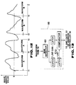
- Fig. 12 shows a waveform of one period.
- the waveforms A and B may consist of a plurality of periods.
- a pitch change instruction is issued from the CPU 24, and the change register CR is switched from "0" to "1".
- address data indicating the waveform B to be switched are output to the corresponding latches, as described above.
- the data latch signal is output from the AND gate 52, and the waveform to be read out is switched to the waveform B. Thereafter, a musical tone is output with a pitch designated in a compass of the waveform B.
- a waveform is switched when a value of waveform data of a musical tone in generation falls within a range of predetermined threshold values.
- waveform data may be switched at a timing of reading out zero-level waveform data, i.e., a timing of reading out waveform data at a zero-crossing point (in Fig. 12, the loop end address coincides with one of zero-crossing points).
- Fig. 13 is a block diagram of a detector as a principal part of this embodiment. In a simplest known method of detecting a zero-crossing point, it is checked if the positive/negative codes of two waveform data corresponding to two adjacent addresses of storage areas in a PCM waveform memory 30 are inverted.
- a detector 60 comprises an MSB detector 62 for detecting the MSB of waveform data in the waveform ROM 30, latches LA5 and LA6 for latching a code bit from the MSB detector, a latch LA7 for latching the output from the latch LA5, and a comparator C2 for comparing the outputs from the latches LA7 and LA6.
- the code bit as the MSB of the waveform data from the waveform ROM 30 is latched by the latches LA5 and LA6.
- new MSB data is latched by the latches LA5 and the LA6, and the latch LA7 latches the immediately preceding code bit previously latched by the latch LA5.
- the comparator C2 compares the contents of the latches LA6 and LA7, i.e., a code bit of waveform data currently read out from the waveform ROM 30 and the immediately preceding code bit.
- the comparator C2 When a coincidence between the two bits is found, i.e., when a zero-crossing point is not detected, the comparator C2 outputs "0"; when a noncoincidence between the two codes is found, i.e., when a zero-crossing point is detected, it outputs "1".
- This output is input to the AND gate 52 of the address controller 26 shown in Fig. 10.
- the waveform data switching operation is executed, as described above.
- Fig. 14 is a block diagram of a musical tone signal generating apparatus according to the fifth embodiment of the present invention.
- An input circuit 20 comprises a pitch designation input section 22a, and a variable pitch input section 22b. If an electronic musical instrument of this embodiment is a keyboard instrument, the pitch designation input section 22a is a keyboard; if it is a wind instrument, a guitar, or the like, the section 22a is an input section such as corresponding switches or frets for inputting pitches.
- the variable pitch input section 22b is, e.g., a switch, a bender, various sensors, or the like for changing and inputting a pitch of a musical tone in generation, and for designating to switch a waveform of a pitch of a musical tone in generation.
- the outputs from the pitch designation input section 22a and the variable pitch input section 22b are input to a CPU 24 as a control circuit.
- the output from the CPU 24 is supplied to a level controller 70 for cross-fade controlling a level of an amplitude of an output waveform according to the designated pitch (to be described later), and is also supplied to address controllers 26a and 26b and envelope generators 28a and 28b.
- the outputs from the address controllers 26a and 26b are respectively supplied to waveform memories (waveform ROMs) 30a and 30b.
- the envelope generators 28a and 28b generate data for changing an amplitude of an output musical tone along with time.
- the waveform ROMs 30a and 30b store waveforms including loop portions in units of predetermined compasses (e.g., in units of octaves).
- the output from the waveform ROM 30a is input to a multiplier 34a together with the output from the envelope generator 28a, and a product from the multiplier 34a is input to a multiplier 72a.
- the multiplier 72a receives the product from the multiplier 34a, and the output from the level controller 70.
- the output from the waveform ROM 30b is input to a multiplier 34b together with the output from the envelope generator 28b, and a product from the multiplier 34b is input to a multiplier 72b.
- the multiplier 72b receives the product from the multiplier 34b and the inverted output of the level controller 70 through an inverter 73.
- the products from the multipliers 72a and 72b are respectively supplied to latches 74a and 74b, and are then output to an adder 76.
- the sum from the adder 76 is output to a latch 36, and is then supplied to a D/A converter 38.
- the analog signal from the D/A converter 38 is amplified by an amplifier 40, and is then output from a loudspeaker (not shown).
- Fig. 15 shows, e.g., the address controller 26a.
- the output of the CPU 24 is connected to a loop start address register LSA, a start address register SA, a pitch register PD, a loop end address register LE, and an end address register EA.
- the output from the start address register SA is input to a current address register CA through a gate G1 which is controlled by the output from the CPU 24.
- the output from the current address register CA and the output from the pitch register PD are input to an adder AD.
- the sum from the adder AD is then output to a latch LA.
- a current address as the output of the latch LA is input to a comparator C0 together with the output from the loop end address register LEA.
- the output of the comparator C0 goes to "1"; otherwise, it goes to "0".
- the output from the latch LA is input to the current address register CA through a gate G3 which is controlled by the output from the comparator C0 and a gate G2 which is ON-controlled through an inverter I1 when a note ON signal (one-shot signal) from the CPU 24 is OFF (at low level).
- the output from the comparator C0 is input to an AND gate 44 together with the output from a comparator C1 via an inverter I4.
- the comparator C1 compares the output from the latch LA and the output from the end address register EA. When the current address is smaller than the end address, the output of the comparator C1 goes to "1"; otherwise, it goes to "0".
- the output from the comparator C1 through an inverter I5 is input to an AND gate 46 together with the output from the comparator C0 through the inverter I4.
- the AND gates 44 and 46 are connected to gates G14 and G15 so as to supply the output from the loop start address register LSA and the output from the current address register CA to the current address register CA. Therefore, the output from the loop start address register LSA is input to the current address register CA through the gates G14 and G2.
- Figs. 16A and 16B show waveforms stored in the waveform ROMs 30a and 30b.
- the waveform ROMs 30a and 30b alternately store waveforms of adjacent compasses in units of octaves.
- the waveform ROM 30a stores waveform data 2 and 4
- the waveform ROM 30b store waveform data 1 and 3 (Fig. 17).
- Figs. 16A and 16B show waveforms of adjacent compasses. Time is plotted along the abscissa, and an amplitude is plotted along the ordinate.
- ST2, ST1, LS2, LS2, LE2, LE1, ED2, and ED1 respectively indicate the start, loop start, loop end, and end addresses stored in the registers SA, LSA, LE, and EA. Attack portions with emphasized tone quality are included between the start addresses ST2 and ST1 and the loop start addresses LS2 and LS1, of the waveforms 2 and 1, as shown in Figs. 16A and 16B, and are also included between the start addresses and the loop start addresses of the waveforms 3 and 4.
- Fig. 17 shows the relationship among adjacent compasses.
- a compass corresponding to pitches C3 to B3 is determined as the waveform 1
- a compass corresponding to pitches C4 to B4 is determined as the waveform 2
- a compass corresponding to pitches C5 to B5 is determined as the waveform 3
- a compass corresponding to pitches C6 to B6 is determined as the waveform 4.
- These items of waveform data are used for compasses designated by a low-key position (LK) and a high-key position (HK). More specifically, in the waveform 1, a pitch C3 corresponds to LK1 and a pitch B3 corresponds to HK1.
- a pitch C4 corresponds to LK2 and a pitch B4 corresponds to HK2.
- Each waveform is addressed by the start address (ST), the end address (ED), the loop start address (LS), and the loop end address (LE).
- a pitch between the pitches B3 and C4 is output under the cross-fade control so that the levels of the waveforms 1 and 2 cross each other. More specifically, as the level of the waveform 1 gradually increases or decreases, the level of the waveform 2 gradually decreases (or increases) accordingly. In this manner, an interval wherein levels of two adjacent waveforms are changed is determined as a cross-fade interval.
- the cross-fade interval is determined to be 100 ⁇ (cent) to have widths of 50 ⁇ from a point at which levels (mixing ratios) of the adjacent waveforms are equal to each other.
- a 100 ⁇ interval between the pitches B3 and C4 is determined as the cross-fade interval.
- the width of this interval is not limited to 100 ⁇ .
- the inclination of the mixing levels representing that cross-fade control is made within 100 ⁇ determined based on the output from the level controller 70.
- the pitch designation input section 22a designates and inputs a desired pitch.
- data (Parameter) for reading out the waveform data corresponding to the designated pitch is set in the address controllers 26a and 26b (step A1).
- the CPU 24 determines one of the waveform data 1 to 4 to which the pitch designated and input by the pitch designation input section 22a belongs.
- the waveform ROMs 30a and 30b alternately store waveform data of adjacent compasses in units of octaves, the CPU 24 also determines, based on the designated pitch, a waveform ROM from which a waveform is to be read out. Parameters corresponding to the designated pitch are set in the address controllers 26a and 26b so as to read out the corresponding waveform data.
- LS2, ST2, LE2, and ED2 are respectively set in the loop start address register LSA, the start address register SA, the loop end address register LE, and the end address register EA of the address controller 26a.
- LS1, ST1, LE1, and ED1 are respectively set in the loop start address register, the start address register, the loop end address register, and the end address register of the address controller 26b in the same manner as the address controller 26a.
- an input specific one of the pitches C4 to B4 of the waveform 2 is set in the pitch register PD.
- a maximum value of a level is set in the level controller 70 to maximize the amplitude of the waveform (step A2). More specifically, the multiplier 72a receives the maximum value from the level controller 70, and the multiplier 72b receives a minimum value (0) obtained by inverting the output from the level controller 70 by the inverter 73.
- the CPU 24 outputs a musical tone generation instruction signal (note ON signal) to the address controller 26a and the envelope generator 28a (step B3). Note that when the compass corresponding to the designated pitch is the waveform 1 or 3, the minimum value is set in the level controller 70 to output the waveform in the waveform ROM 30b at the maximum level.
- the gate G1 When the note ON signal is output from the CPU 24, the gate G1 is enabled and the output ST2 is input from the start address register SA to the current address register CA in address controller 26.
- the output from the current address register CA is input to the adder AD together with the output from the pitch register PD.
- the sum from the adder AD is output to the latch LA.
- a value which is incremented and stored in the latch LA is equal to the sum of the output from the current address register CA and the pitch value output from the pitch register PD by the adder AD at a predetermined timing (sampling period).
- the output from the latch LA incremented by the pitch value is supplied to the comparator C0, and is fed back to the current address register CA through the gate G3 controlled by the output from the comparator C0 and the gate G2.
- the gate G2 is enabled by the output from the comparator C0.
- the gate G2 is enabled immediately after the gate G1 is enabled in response to the note ON signal and the output from the start address register SA is input to the current address register CA.
- the current address stored in the latch LA is kept incremented by a loop of the latch LA, the gates G3 and G2, the current address register CA, and the adder AD until the current address in the latch LA reaches the loop end address LE2.
- the current address is supplied to the waveform ROM 30a as a read address. Since the incrementing rate of the current address is determined by the output from the pitch register PD, pitch control can be realized.
- the output from the comparator C0 disables the gate G3, and is input to one input terminal of each of the AND gates 44 and 46 via the inverter I4.
- the outputs from the AND gates 44 and 46 are determined by the output from the comparator C1. More specifically, the comparator C1 makes a comparison to determine whether or not the current address stored in the latch LA has reached the output value ED2 from the end address register EA. This output is input to the other input terminal of the AND gate 44, and is also input to the other input terminal of the AND gate 46 through an inverter I5.
- the AND gate 44 When the current address falls within the range of the loop end address LE2 and the end address ED2, the AND gate 44 outputs a loop end signal to enable the gate G14 so as to allow the output LS2 of the loop start address register LS to pass the gate G14. Since no end signal is output from the AND gate 46, the gate G15 is kept disabled. More specifically, the output LS2 of the loop start address register LS is output to the current address register CA through the gates G14 and G2. When the current address reaches the loop end address LE2, it returns to the loop start address LS2 to form a loop period (LS2 to LE2). In this manner, addressing in this loop period is repeated to continuously output a musical tone. Therefore, of the waveform 2 in Fig.
- waveform data read out from the waveform ROM 30a is supplied to the multiplier 34a.
- Predetermined envelope data generated by the envelope generator 28a which received the note ON signal from the CPU 24 is supplied to the multiplier 34a.
- the waveform data read out from the waveform ROM 30a is multiplied with the predetermined envelope data generated by the envelope generator 28a by the multiplier 34a, and the product is then output to the multiplier 72a.
- the maximum value is multiplied with the output from the multiplier 34a by the multiplier 72a, and the product is then output through the adder 76, the latch 36, and the like.
- step A4 After the note ON signal is output in step A3, it is checked if a control signal is input to change a pitch of a musical tone in generation, i.e., frequency by the variable pitch input section 22b (step A4).
- the change in pitch can be detected by monitoring the variable pitch input section 22b by the CPU 24.
- step A4 the same judgment is made until the pitch is changed.
- step A5 If it is determined in step A5 that the pitch is changed downward, the flow advances to step A6 to check if the pitch is changed downward for the first time. If YES in step A6, the flow advances to step A7, and waveform addresses of the loop section of waveform data adjacent to the compass of the waveform 2 are set in the address controller 26b in this case.
- the address controller 26a is operated in the same manner as the address controller 26a to read out the loop period of waveform data adjacent to the compass of the waveform 2.
- waveform data of the loop period of the adjacent compass (waveform 1 in this case) is read out to the address controller 26a.
- the loop start address LS1 is set in the start address register.
- waveform data in the loop period of the waveform 1 between the loop start address LS1 and the loop end address LE1 shown in Fig. 16B is read out from the waveform ROM 30b.
- the waveform data of the loop period of the waveform 1 read out from the waveform ROM 30b by the address controller 26b is supplied to the multiplier 34b.
- a predetermined envelope data generated by the envelope generator 28b which received the note ON signal from the CPU 24 is supplied to the multiplier 34b.
- the predetermined envelope data generated by the envelope generator 28b is multiplied with the waveform data read out from the waveform ROM 30b by the multiplier 34b, and the product is then output to the multiplier 72b. If it is determined in step A6 that the pitch is changed for the second time or thereafter, the flow advances not to step A7 but to step A8.
- a change in pitch is determined in step A8.
- the pitch of the low key LK2 is C4
- the level controller 70 Since the value of the level controller 70 is changed depending on a pitch, a mixing ratio of the waveform data 1 and 2 is determined depending on a pitch in this case. Therefore, if the pitch is C4 or more, a musical tone is generated using only the waveform data 2, as described above. However, if the pitch is changed from C4 toward B3, the level of the waveform 2 is changed from the maximum value to the minimum value, while the level of the loop period of the waveform data 1 is changed from the minimum value to the maximum value, thus achieving the cross-fade control. Since the level controller 70 supplies its output to the multiplier 72b, and the multiplier 72b receives the output inverted by the inverter 73, if one level is increased, the other level is complementarily decreased.
- step A4 every time a change in pitch is detected in step A4, steps A5, A6, A8, and A9 are executed, and a series of processing operations are repeated until step A10 is satisfied.
- step A10 a change in pitch is judged again to check if a pitch ⁇ LK2 - 100 ⁇ .
- step A9 a change in pitch is judged again to check if a pitch ⁇ LK2 - 100 ⁇ .
- step A9 a change in pitch is judged again to check if a pitch ⁇ LK2 - 100 ⁇ .
- step A9 a change in pitch is judged again to check if a pitch ⁇ LK2 - 100 ⁇ .
- step A9 when another waveform is switched after the cross-fade control is made in step A9, e.g., after a compass is switched from that of the waveform 2 to that of the waveform 1, YES is determined in step A10, and the flow advances to step A11.
- NO is determined in step A8, as a matter of course.
- step A11 the previous address controller (26a in this case) is set OFF, i.e., initialized. Thereafter, the waveform 1 is output with
- step A5 if an upward pitch change is detected in step A5, the flow advances to step A12 to check if the pitch is changed upward for the first time. If YES in step A12, the flow advances to step A13, parameters are set in the address controller 26b to read out waveform data adjacent to the compass of the waveform 2, in this case, the waveform of the loop period of the waveform 3, and the note ON signal is output in the same manner as for the waveform 2. If NO in step A12, the flow advances not to step A13 but to step A14.
- step A14 a change in pitch is determined.
- the high key HK2 is B4, it is checked if a pitch is present between B4 and C5, i.e., if HK ⁇ pitch ⁇ HK + 100 ⁇ is satisfied. If NO in step A14, the flow advances to step A16 (to be described later). However, if YES in A14, the flow advances to step A15 to perform mixing control under the cross-fade control. More specifically, the value of the level controller 70 is changed depending on the pitch. In this case, the mixing ratio of the waveform and the loop period of the waveform 3 is determined depending on the pitch.
- the level of the waveform 2 is changed from the maximum value to the minimum value, while the level of the waveform of the loop period of the waveform 3 to be mixed under the cross-fade control is changed from the maximum value to the minimum value.
- the level of a musical tone of the waveform 2 is decreased, and the level of a musical tone of the waveform of the loop interval of the waveform 3 is increased, thus switching the waveforms.
- step A16 a change in pitch is judged in the same manner as in step A10. In this case, it is checked if the pitch ⁇ HK2 + 100 ⁇ .
- step A17 the previous address controller (26a in this case) is set OFF, i.e., initialized. Thereafter, only the waveform data 3 is output with the designated pitch.
- a plurality of items of PCM waveform data are stored in the PCM waveform memory by dividing areas.
- the PCM waveform memory may store only one PCM waveform data common to all the compasses.
- the present invention can be applied to any other apparatuses which express waveforms without using the PCM technique.
- a differential PCM method for example, a differential PCM method, an adaptive differential PCM method, a delta modulation method, and the like may be employed.
- waveform data previously read out from the waveform ROM is determined as the waveform A, and waveform data to be switched is determined as the waveform B.
- waveform data to be switched is determined as the waveform B.
- the present invention is not limited to this. Arbitrary waveform data can be read out, as a matter of course.
- items of waveform data of adjacent compasses are alternately stored in two waveform ROMs in units of octaves.
- these waveform ROMs may store waveforms of all the compasses.
- the address controller 26a can be started first for any compass.
- the two systems of musical tone generators are not limited to the embodiments described above, but may be realized by time-divisionally using two channels of a multichannel sound source. That is, at least two musical tone generation channels need only be prepared to generate one tone, and the structure of each musical tone generation channel is not limited.
- Envelope control by the envelope generator may be performed after the adder 76 in Fig. 14. In this case, one envelope generator can be used, thus further simplifying the arrangement.
Landscapes
- Engineering & Computer Science (AREA)
- Physics & Mathematics (AREA)
- Acoustics & Sound (AREA)
- Multimedia (AREA)
- General Engineering & Computer Science (AREA)
- Electrophonic Musical Instruments (AREA)
Claims (11)
- Un dispositif de génération de signaux de sons musicaux, comprenant :
des moyens de mémoire (8, 30) pour enregistrer différentes données de forme d'onde en correspondance avec un ensemble de différentes plages de sons;
des moyens d'actionnement de désignation de hauteur (5, 20) pour désigner une hauteur d'un son musical;
des moyens de désignation de forme d'onde (24) pour désigner, à partir des moyens de mémoire (8, 30), des données de forme d'onde correspondant à une plage de sons à laquelle appartient la hauteur qui est désignée par les moyens d'actionnement de désignation de hauteur (5, 20);
des moyens de lecture (1, 26) pour lire les données de forme d'onde qui sont désignées par les moyens de désignation de forme d'onde (24), à une vitesse correspondant à la hauteur qui est désignée par les moyens d'actionnement de désignation de hauteur (5, 20); et
des moyens d'émission de signal de son musical (7, 34) pour produire un signal de son musical sur la base des données de forme d'onde qui sont lues par les moyens de lecture (26);
caractérisé en ce qu'il comprend en outre :
des moyens de génération de signal de temps (32, 60, CO), qui fonctionnent lorsqu'une hauteur courante d'un signal de son musical en cours de génération est changée par les moyens d'actionnement de désignation de hauteur (5, 20), pour devenir une nouvelle hauteur appartenant à une nouvelle plage de sons qui est différente d'une plage de sons courante à laquelle appartient la hauteur courante, ces moyens de génération de signal de temps (32) comprenant des moyens pour détecter si une valeur des données de forme d'onde qui sont lues dans les moyens de mémoire (8, 30) tombe ou non dans une plage prédéterminée, et émettant un signal de temps de commutation lorsque la valeur des données de forme d'onde tombe à l'intérieur de la plage prédéterminée; et
des moyens de commutation (CR, CT1) pour faire en sorte que les moyens de lecture (26) lisent des données de forme d'onde correspondant à la nouvelle plage de sons à laquelle appartient la nouvelle hauteur désignée par les moyens d'actionnement de désignation de hauteur (5, 20), sous l'action du signal de temps de commutation qui est produit par les moyens de génération de signal de temps (32, 60, CO). - Un dispositif selon la revendication 1, caractérisé en ce que les moyens d'actionnement de désignation de hauteur (5, 20) comprennent des moyens de désignation de hauteur (22a) pour désigner une hauteur correspondant à une gamme, et des moyens d'entrée variables (22b) pour faire varier la hauteur d'un son musical en cours de génération.
- Un dispositif selon la revendication 1 ou 2, caractérisé en ce que les moyens de génération de signal de temps (32) émettent le signal de temps de commutation en détectant un instant auquel les moyens de lecture (24) lisent des données de forme d'onde de niveau zéro.
- Un dispositif selon l'une quelconque des revendications précédentes, caractérisé en ce que les moyens de mémoire (8, 30) conservent des données de forme d'onde en modulation par impulsions et codage.
- Un dispositif selon l'une quelconque des revendications précédentes, caractérisé en ce que les moyens de commutation (CR) comprennent en outre des moyens de commutation de vitesse de lecture (CT2) pour faire en sorte que les moyens de lecture (1) passent de la vitesse correspondant à la hauteur courante désignée par les moyens d'actionnement de désignation de hauteur (5), à la vitesse correspondant à la nouvelle hauteur, sous l'effet du signal de temps de commutation qui provient des moyens de génération de signal de temps (CO).
- Un dispositif selon l'une quelconque des revendications précédentes, caractérisé en ce que chacune des données de forme d'onde qui sont enregistrées dans les moyens de mémoire (8) comprend une partie de boucle qui est lue de façon répétée.
- Un dispositif selon la revendication 6, caractérisé en ce que les moyens de génération de signal de temps (CO) émettent le signal de temps de commutation lorsque les données de forme d'onde à une adresse de fin de boucle sont lues dans les moyens de mémoire (8).
- Un dispositif selon l'une quelconque des revendications précédentes, caractérisé en ce que les moyens de lecture (26) comprennent deux moyens de lecture (26a, 26b), un premier de ces deux moyens de lecture (26a, 26b) lisant des données de forme d'onde courantes dans les moyens de mémoire (30), et le second des deux moyens de lecture (26a, 26b) lisant de nouvelles données de forme d'onde dans les moyens de mémoire (30), sur la base de la commande des moyens de commutation (CR), des moyens de commande d'amplitude (70) pour diminuer progressivement jusqu'à zéro la valeur des données de forme d'onde courantes qui sont lues par le premier des deux moyens de lecture (26a, 26b), et pour augmenter progressivement la valeur des nouvelles données de forme d'onde qui sont lues par le second des deux moyens de lecture (26a, 26b), sous la dépendance du signal de temps de commutation qui est produit par les moyens de génération de signal de temps (32), et des moyens de mélange (76) pour mélanger les deux sortes de données de forme d'onde après qu'elles ont fait l'objet d'une commande d'amplitude par les moyens de commande d'amplitude (70).
- Un dispositif selon la revendication 8, caractérisé en ce que les moyens d'actionnement de désignation de hauteur (5, 20) comprennent des moyens de désignation de gamme (22a) pour désigner une hauteur correspondant à une gamme, et des moyens de variation de hauteur (22b) pour faire varier la hauteur d'un son musical en cours de génération.
- Un dispositif selon la revendication 8 ou 9, caractérisé en ce que les moyens de mémoire (8, 30) comprennent des premiers et des seconds moyens de mémoire (30a, 30b) pour enregistrer des données de forme d'onde correspondant à des plages de sons adjacentes.
- Un dispositif selon la revendication 8, caractérisé en ce que les données de forme d'onde qui sont enregistrées dans les moyens de mémoire (8, 30) comprennent chacune une partie d'attaque et une partie de boucle qui est lue de façon répétée, et lorsque les moyens de lecture (26) lisent de nouvelles données de forme d'onde, les moyens de lecture de forme d'onde lisent seulement la partie de boucle des nouvelles données de forme d'onde.
Applications Claiming Priority (6)
| Application Number | Priority Date | Filing Date | Title |
|---|---|---|---|
| JP1024025A JP2591138B2 (ja) | 1989-02-03 | 1989-02-03 | 波形データ読出装置 |
| JP24025/89 | 1989-02-03 | ||
| JP1033535A JP2893698B2 (ja) | 1989-02-15 | 1989-02-15 | 楽音信号発生装置 |
| JP33535/89 | 1989-02-15 | ||
| JP1120750A JPH02300797A (ja) | 1989-05-15 | 1989-05-15 | 楽音生成装置 |
| JP120750/89 | 1989-05-15 |
Publications (3)
| Publication Number | Publication Date |
|---|---|
| EP0381159A2 EP0381159A2 (fr) | 1990-08-08 |
| EP0381159A3 EP0381159A3 (fr) | 1991-02-20 |
| EP0381159B1 true EP0381159B1 (fr) | 1995-04-26 |
Family
ID=27284486
Family Applications (1)
| Application Number | Title | Priority Date | Filing Date |
|---|---|---|---|
| EP90101837A Expired - Lifetime EP0381159B1 (fr) | 1989-02-03 | 1990-01-30 | Dispositif générateur de son musical |
Country Status (3)
| Country | Link |
|---|---|
| US (1) | US5069105A (fr) |
| EP (1) | EP0381159B1 (fr) |
| DE (1) | DE69018844T2 (fr) |
Families Citing this family (9)
| Publication number | Priority date | Publication date | Assignee | Title |
|---|---|---|---|---|
| JP2792368B2 (ja) * | 1992-11-05 | 1998-09-03 | ヤマハ株式会社 | 電子楽器 |
| DE69732311T2 (de) | 1996-11-27 | 2006-01-05 | Yamaha Corp., Hamamatsu | Verfahren zur Erzeugung von Musiktönen |
| JP3451900B2 (ja) * | 1997-09-22 | 2003-09-29 | ヤマハ株式会社 | ピッチ/テンポ変換方法及び装置 |
| JP3744216B2 (ja) * | 1998-08-07 | 2006-02-08 | ヤマハ株式会社 | 波形形成装置及び方法 |
| JP4448378B2 (ja) * | 2003-07-30 | 2010-04-07 | ヤマハ株式会社 | 電子管楽器 |
| JP2005049439A (ja) * | 2003-07-30 | 2005-02-24 | Yamaha Corp | 電子楽器 |
| DE602006000117T2 (de) * | 2005-06-17 | 2008-06-12 | Yamaha Corporation, Hamamatsu | Musiktonwellenformsynthesizer |
| JP5233416B2 (ja) * | 2008-05-29 | 2013-07-10 | 富士通株式会社 | 信号波形生成回路及び信号波形生成方法 |
| JP6019803B2 (ja) * | 2012-06-26 | 2016-11-02 | ヤマハ株式会社 | 自動演奏装置及びプログラム |
Family Cites Families (13)
| Publication number | Priority date | Publication date | Assignee | Title |
|---|---|---|---|---|
| GB1558280A (en) * | 1975-07-03 | 1979-12-19 | Nippon Musical Instruments Mfg | Electronic musical instrument |
| JPS52121313A (en) * | 1976-04-06 | 1977-10-12 | Nippon Gakki Seizo Kk | Electronic musical instrument |
| JPS6029959B2 (ja) * | 1977-11-08 | 1985-07-13 | ヤマハ株式会社 | 電子楽器 |
| JPS5635192A (en) * | 1979-08-31 | 1981-04-07 | Nippon Musical Instruments Mfg | Electronic musical instrument |
| US4352312A (en) * | 1981-06-10 | 1982-10-05 | Allen Organ Company | Transient harmonic interpolator for an electronic musical instrument |
| US4463650A (en) * | 1981-11-19 | 1984-08-07 | Rupert Robert E | System for converting oral music to instrumental music |
| US4597318A (en) * | 1983-01-18 | 1986-07-01 | Matsushita Electric Industrial Co., Ltd. | Wave generating method and apparatus using same |
| JPS6029793A (ja) * | 1983-07-28 | 1985-02-15 | ヤマハ株式会社 | 楽音形成装置 |
| US4633749A (en) * | 1984-01-12 | 1987-01-06 | Nippon Gakki Seizo Kabushiki Kaisha | Tone signal generation device for an electronic musical instrument |
| JPS6145297A (ja) * | 1984-08-09 | 1986-03-05 | カシオ計算機株式会社 | 電子楽器 |
| JPH0789279B2 (ja) * | 1985-10-21 | 1995-09-27 | ヤマハ株式会社 | 楽音信号発生装置 |
| EP0274137B1 (fr) * | 1987-01-07 | 1993-07-21 | Yamaha Corporation | Dispositif générateur de son comprenant une fonction de stockage numérique de son |
| JPH0823746B2 (ja) * | 1987-05-22 | 1996-03-06 | ヤマハ株式会社 | 自動楽音発生装置 |
-
1990
- 1990-01-29 US US07/471,835 patent/US5069105A/en not_active Expired - Lifetime
- 1990-01-30 DE DE69018844T patent/DE69018844T2/de not_active Expired - Lifetime
- 1990-01-30 EP EP90101837A patent/EP0381159B1/fr not_active Expired - Lifetime
Also Published As
| Publication number | Publication date |
|---|---|
| EP0381159A2 (fr) | 1990-08-08 |
| EP0381159A3 (fr) | 1991-02-20 |
| DE69018844D1 (de) | 1995-06-01 |
| DE69018844T2 (de) | 1995-11-30 |
| US5069105A (en) | 1991-12-03 |
Similar Documents
| Publication | Publication Date | Title |
|---|---|---|
| HK134395A (en) | Tone signal generation device having a tone sampling function | |
| EP0381159B1 (fr) | Dispositif générateur de son musical | |
| EP0167847B1 (fr) | Dispositif générateur de son | |
| US5146834A (en) | Interpolating tone wave generator having truncated data | |
| US5264657A (en) | Waveform signal generator | |
| JP2559209B2 (ja) | 楽音信号発生装置 | |
| US5109746A (en) | Envelope generator for use in an electronic musical instrument | |
| US5886278A (en) | Apparatus for reducing change in timbre at each point where tone ranges are switched | |
| US5284080A (en) | Tone generating apparatus utilizing preprogrammed fade-in and fade-out characteristics | |
| JPH0428319B2 (fr) | ||
| US5022304A (en) | Musical tone signal generating apparatus | |
| US8067684B2 (en) | Filter device and electronic musical instrument using the filter device | |
| JP2560817B2 (ja) | 波形データ読出装置 | |
| JPH067327B2 (ja) | 楽音発生装置のパラメータ設定装置 | |
| JP2947525B2 (ja) | エンベロープ発生器 | |
| JP2621458B2 (ja) | 波形読み出し装置 | |
| JP2625669B2 (ja) | 楽音波形発生装置 | |
| JP2893698B2 (ja) | 楽音信号発生装置 | |
| JP2591138B2 (ja) | 波形データ読出装置 | |
| JP2970438B2 (ja) | 波形メモリ型楽音発生装置 | |
| JP3543203B2 (ja) | 電子楽器 | |
| US5559300A (en) | Delay time modulation effecting apparatus for processing musical tone signal | |
| JP3106051B2 (ja) | 電子楽器 | |
| JP3504387B2 (ja) | 電子楽器 | |
| JPH038558B2 (fr) |
Legal Events
| Date | Code | Title | Description |
|---|---|---|---|
| PUAI | Public reference made under article 153(3) epc to a published international application that has entered the european phase |
Free format text: ORIGINAL CODE: 0009012 |
|
| AK | Designated contracting states |
Kind code of ref document: A2 Designated state(s): DE FR GB IT |
|
| PUAL | Search report despatched |
Free format text: ORIGINAL CODE: 0009013 |
|
| AK | Designated contracting states |
Kind code of ref document: A3 Designated state(s): DE FR GB IT |
|
| 17P | Request for examination filed |
Effective date: 19910321 |
|
| 17Q | First examination report despatched |
Effective date: 19920814 |
|
| GRAA | (expected) grant |
Free format text: ORIGINAL CODE: 0009210 |
|
| AK | Designated contracting states |
Kind code of ref document: B1 Designated state(s): DE FR GB IT |
|
| ITF | It: translation for a ep patent filed | ||
| REF | Corresponds to: |
Ref document number: 69018844 Country of ref document: DE Date of ref document: 19950601 |
|
| ET | Fr: translation filed | ||
| PLBE | No opposition filed within time limit |
Free format text: ORIGINAL CODE: 0009261 |
|
| STAA | Information on the status of an ep patent application or granted ep patent |
Free format text: STATUS: NO OPPOSITION FILED WITHIN TIME LIMIT |
|
| 26N | No opposition filed | ||
| REG | Reference to a national code |
Ref country code: GB Ref legal event code: IF02 |
|
| PGFP | Annual fee paid to national office [announced via postgrant information from national office to epo] |
Ref country code: DE Payment date: 20090123 Year of fee payment: 20 |
|
| PGFP | Annual fee paid to national office [announced via postgrant information from national office to epo] |
Ref country code: GB Payment date: 20090128 Year of fee payment: 20 |
|
| PGFP | Annual fee paid to national office [announced via postgrant information from national office to epo] |
Ref country code: IT Payment date: 20090127 Year of fee payment: 20 |
|
| PGFP | Annual fee paid to national office [announced via postgrant information from national office to epo] |
Ref country code: FR Payment date: 20090113 Year of fee payment: 20 |
|
| REG | Reference to a national code |
Ref country code: GB Ref legal event code: PE20 Expiry date: 20100129 |
|
| PG25 | Lapsed in a contracting state [announced via postgrant information from national office to epo] |
Ref country code: GB Free format text: LAPSE BECAUSE OF EXPIRATION OF PROTECTION Effective date: 20100129 |
|
| PG25 | Lapsed in a contracting state [announced via postgrant information from national office to epo] |
Ref country code: DE Free format text: LAPSE BECAUSE OF EXPIRATION OF PROTECTION Effective date: 20100130 |