EP0382580B1 - Bildverarbeitungsgerät - Google Patents
Bildverarbeitungsgerät Download PDFInfo
- Publication number
- EP0382580B1 EP0382580B1 EP19900301475 EP90301475A EP0382580B1 EP 0382580 B1 EP0382580 B1 EP 0382580B1 EP 19900301475 EP19900301475 EP 19900301475 EP 90301475 A EP90301475 A EP 90301475A EP 0382580 B1 EP0382580 B1 EP 0382580B1
- Authority
- EP
- European Patent Office
- Prior art keywords
- data
- object pixel
- error
- input
- average density
- Prior art date
- Legal status (The legal status is an assumption and is not a legal conclusion. Google has not performed a legal analysis and makes no representation as to the accuracy of the status listed.)
- Expired - Lifetime
Links
Images


Classifications
-
- H—ELECTRICITY
- H04—ELECTRIC COMMUNICATION TECHNIQUE
- H04N—PICTORIAL COMMUNICATION, e.g. TELEVISION
- H04N1/00—Scanning, transmission or reproduction of documents or the like, e.g. facsimile transmission; Details thereof
- H04N1/40—Picture signal circuits
- H04N1/40087—Multi-toning, i.e. converting a continuous-tone signal for reproduction with more than two discrete brightnesses or optical densities, e.g. dots of grey and black inks on white paper
-
- H—ELECTRICITY
- H04—ELECTRIC COMMUNICATION TECHNIQUE
- H04N—PICTORIAL COMMUNICATION, e.g. TELEVISION
- H04N1/00—Scanning, transmission or reproduction of documents or the like, e.g. facsimile transmission; Details thereof
- H04N1/40—Picture signal circuits
- H04N1/405—Halftoning, i.e. converting the picture signal of a continuous-tone original into a corresponding signal showing only two levels
- H04N1/4051—Halftoning, i.e. converting the picture signal of a continuous-tone original into a corresponding signal showing only two levels producing a dispersed dots halftone pattern, the dots having substantially the same size
- H04N1/4052—Halftoning, i.e. converting the picture signal of a continuous-tone original into a corresponding signal showing only two levels producing a dispersed dots halftone pattern, the dots having substantially the same size by error diffusion, i.e. transferring the binarising error to neighbouring dot decisions
Definitions
- the present invention relates to an image processing apparatus for quantizing image data into multi-level data such as ternary or quaternary data.
- the former method has been proposed, for example, from Page 36 to Page 37 in "An Adaptive Algorithm for Spatial Gray Scale", SID 75 Digest by R. Floyd & L. Steinberg.
- multi-level image data on an object pixel is binarized (converted into the highest density level or lowest density level). Thereafter, an error between the thus-obtained binary level and the multi-level image data which is not yet binarized is weighted, and this weighted error is added to data on the pixels in the vicinity of the object pixel.
- the aforementioned error diffusion method involves correction of an error between image data which is input and image data which is output.
- the density of the input image and of the output image can be stored, and this enables provision of images which are excellent in both resolution and gradation.
- JP-A-60-214160 discloses calculating an average value from the input data, this value then being quantised.
- EP-A-0248616 discloses a similar procedure.
- An embodiment thereof provides an image processing apparatus which employs a reduced amount of data to be processed for multi-level conversion, which has a simple hardware configuration required for multi-level conversion, and which ensures that an image obtained has excellent gradation and resolution.
- An embodiment of the present invention provides an image processing apparatus which comprises an input means for inputting data on an object pixel, a calculation means for calculating an average density value for a predetermined area, a multi-level conversion means for converting the data on the object pixel into multi-level data on the basis of the average density value obtained by the calculation means, and a correction means for correcting an error generated when the data on the object pixel is converted into the multi-level data.
- An embodiment of the present invention provides an image processing data which comprises an input means for inputting data on an object pixel, a calculation means for calculating an average density value for a predetermined area, a multi-level conversion means for converting the data on the object pixel into multi-level data consisting of a plurality of bits on the basis of the average density value obtained by the calculation means, and a correction means for correcting an error generated when the data on the object pixel is converted into the multi-level data.
- the calculation means calculates the average density value for the predetermined area using data whose bit-width is smaller than that of the multi-level data consisting of the plurality of bits and obtained by the multi-level conversion means.
- An embodiment of the present invention provides an image processing apparatus which enables multi-level conversion providing good gradation and resolution reproduction to be obtained by a small-scale hardware configuration at a high speed.
- An embodiment of the present invention provides an image processing apparatus whose hardware scale is independent from an increase in the number of bits of data to be processed for the multi-level conversion and which thus facilitates expansion toward high-quality images.
- An embodiment of the present invention provides an image processing apparatus which enables the density of an image input and of an image output to be completely stored when the error diffusion method is employed because no division operations are required to diffuse an error and because no quantizing error occurs.
- An embodiment of the present invention provides an image processing apparatus which is capable of a halftone process that can substitute for the error diffusion method at a low cost.
- An embodiment of the present invention provides an image processing apparatus which enables pseudo contours generated by multi-level conversion in the error diffusion method to be prevented so as to ensure a high-quality image.
- An embodiment of the present invention provides an image processing apparatus which is capable of reproducing the density of an image which is faithful to that of an original image utilizing the feature of a recording device.
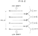
- a reference symbol f (i, j) denotes multi-level density data (any value ranging between 0 to 1) on an input image at an object pixel which is to be quantized into quaternary data. Quaternarization has already been conducted on the pixels located above the broken line. After the quaternarization for the object pixel, the same processing will be conducted on the subsequent pixels in the order of f (i, j+1), f (i, j+2) ...
- a reference symbol B (i, j) denotes a quaternarized density (which may be 0, 1 3 , 2 3 or 1). Quaternarization has already been conducted on the pixels surrounded by the broken line at the time when the object pixel is processed. The data on these pixels are used to quaternarize the object pixel.
- Fig. 1 (3) shows a weighting mask.
- a reference symbol R denotes a weighting mask which is used to obtain an average density and which is expressed in a matrix of 3 x 3.
- the object pixel is converted into four densities ranging from black to white, and average quaternary densities m0 (i,j), m1 (i, j), m2 (i, j), and m3 (i, j) of the vicinity of an object pixel in all the cases are obtained by the following equations:
- Fig. 2 shows M0 to M3, and B which are expressed by Equations (1) to (4).
- E (i, j) denotes an error which is generated when the data f (i, j-1) on the pixel immediately before the object pixel is quaternarized, and which is corrected when the average value of the object pixel is operated.
- the multi-level density data f (i, j) on the object pixel is quaternarized using the average densities m0, m1, m2 and m3 as follows:
- f (i, j) ⁇ m0 (i, j) + m1 (i, j) 2 B(i, j) 0
- E(i, j+1) f(i, j)-m0(i, j) 5 ⁇
- m0(i, j)+m1(i, j) 2 ⁇ f(i,j) ⁇ m1(i, j)+m2(i, j) 2 B(i,j) 1 3
- E(i,j+1) f(i,j)-m1(i,j) 6 ⁇
- the quaternarizing error E (i, j) is an error generated when the multi-level data f (i, j-1) on the pixel immediately before the object pixel is quaternarized. More specifically, to quaternarize the data f (i, j-1) is to approximate that data by either of the average densities m0 (i, j-1), m1 (i, j-1), m2 (i, j-1) and m3 (i, j-1) of the adjacent pixels, and in either case, an error occurs with respect to the data f (i, j-1) which is actually input.
- a high halftone reproduction which cannot be realized in the conventional average density approximation method, can be achieved, because the quaternarizing error E (i, j) generated in the pixel immediately before the object pixel is corrected when the average value of the object pixel is calculated, and quaternarization is conducted on the object pixel using that average value.
- optimal correction can be conducted on the individual levels of the quaternarizing image B (i, j), and quaternarized density of the image can be stored in a complete from over the entire area of the image input.
- this image processing method assures excellent image reproduction even though the quantity of data to be processed is very small. This is because, even though correction of the error E generated by quaternarization is conducted on the adjacent single pixel, the average density values are obtained using the quaternary data, and this ensures the same effect as that provided when the error E is distributed to a plurality of pixels for correction.
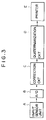
- FIG. 3 is a block diagram of the first embodiment of an image processing apparatus according to the present invention.
- An input sensor portion A is constructed by a photoelectric conversion element such as a CCD device, and a drive device for driving the photoelectric conversion element for scanning.
- the input sensor portion A reads an original.
- the image data on the original which is read by the input sensor portion A is sent to an A/D converter B in sequence, where the data on the individual pixels are converted into 8-bit digital data to obtain data representing any of 256 levels.
- shading or the like is performed digitally by a correction circuit C to correct irregularities in the sensitivity of the CCD sensor or in the illumination of a light source.
- the corrected data is sent to a quaternarization circuit D where the 8-bit multi-level image data are converted into 2-bit quaternary data by the aforementioned image processing method.
- a printer E is a multi-level printer which is capable of reproducing an image on a sheet of paper on the basis of the quaternary data sent from the quaternarization circuit D.
- Fig. 4 is a block diagram of the quaternarization circuit D shown in Fig. 3.
- the quaternarization circuit D is composed of delay RAMs 1 and 2 for storing the quaternary data in a quantity of one line, DF/Fs (flip-flops) 3 to 7 and 11 for delaying the quaternary data by one clock pulse corresponding to one pixel, an average density calculation ROM 8 for calculating the average density of the pixels in the vicinity of the object pixel and outputting a threshold, a substracter 9 for calculating the difference between the input multi-level data on the object pixel and the threshold, a comparator 10 for comparing the threshold which is output from the ROM 8 with the multi-level data on the object pixel, a DF/F 11, a ROM 12 for calculating error data which is to be corrected when the data which is input subsequent to that on the object pixel is quantized into multi-level data, a subtracter 13 for subtracting the error E generated when quaternarization is conducted on the
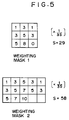
- a weighting mask 1 is a mask used to obtain the average density value from the quaternary data on the total of 9 pixels including the object pixel.
- the weighting mask 1 shown in Fig. 5 is multiplied by 1 3S to convert the 2-bit quaternary data which is stored in the delay RAMs 1 and 2 in the DF/Fs 3 to 7 shown in Fig. 4 and which represents 0, 1, 2 and 3 into 0, 1 3 , 2 3 and 1 expressed in Equations (1) to (4).
- a weighting mask 2 is a modification of the weighting mask 1, which is used to calculate the average density value from the quaternary data on the total of 15 pixels including the object pixel.
- the quaternarizing data B (i, j) is output relative to the input image data f (i, j), and the quaternarizing data B (i, j) is input to the delay RAM 2 and the DF/F 7.
- the quaternarizing data is delayed by one line by the RAM 2 to obtain the quaternary data B (i-1, j+1) and by two lines by the RAM 1 to obtain the quaternary data B (i-2, j+1).
- the output of the dalay RAM 2 is input to the DF/F 5 to obtain the quaternary data B (i-1, j), and the output of the DF/F 5 is then input to the DF/F 6 to obtain the quaternary data B (i-1, j-1).
- the output of the daley RAM 1 is input to the DF/F 3 to obtain the data B (i-2, j), and the output of the DF/F 3 is then output to the DF/F 4 to obtain the data B (i-2, j-1).
- the quaternarizing data B (i, j) is input to the DF/F 7 to obtain the data B (i, j-1).
- the thus-obtained quaternary data are quaternary image signals in the vicinity of the input image f (i, j), as shown in Fig. 1. These quaternary data are input to input addresses of the ROM 8 to obtain the threshold M 0 + 1 6 R shown in Fig. 2 on the basis of Equations (1) and (2).
- This threshold is output to both the comparator 10 and the subtracter 9.
- the subtracter 9 calculates the difference between the two sides of the inequality in Equation (5) and outputs the absolute value thereof to clarify how different the data f(i, j) and the threshold M 0 + 1 6 R shown in Fig. 2 are.
- the comparator 10 outputs to the ROMs 12 and 14 data indicating whether f (i, j) is larger or smaller than the threshold M 0 + 1 6 R.
- the ROM 14 outputs quaternary data B (i, j) using the output of the subtracter 9 (which indicates how different f (i, j) and M 0 + 1 6 R are) and that of the comparator 10 (which indicates as to whether f (i, j) is larger than M 0 + 1 6 R).
- Equation (5) is modified using Equations (1), (9) and (12) as follows:
- B(i,j) 0,
- E(i,j+1) f(i,j) -m0(i,j) 5 ⁇ '
- an error E (i, j+1) associated with the average density value can thus be easily obtained by connecting the output of the subtracter 9 and that of the comparator 10 to the input address terminal of the ROM 12 using the translation table stored in the ROM 12.
- the quaternarizing data B (i, j) can be similarly defined using the translation table which is stored in the ROM 14 by connecting the output of the subtracter 9 and that of the comparator 10 to the input address terminal of the ROM 14, as stated above.
- the DF/F 11 delays the error E (i, j+1) by 1 clock pulse.
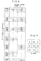
- Fig. 6 shows an example of the table stored in the ROM 12.
- This example employs the weighting mask 1 shown in Fig. 5.
- the values in the average density calculation ROM table are 8-bit data obtained by multiplying the values obtained by Equations (1) to (4) by 255 and normalized to an actually input 8-bit image density level (representing any value ranging from 0 to 255).
- the weighting mask 1 takes the form shown in Fig. 7.
- the hardware structure of this embodiment can be constructed by several RAM, ROM and operation IC chips in a small scale, as shown in Fig. 4. Furthermore, in this embodiment, multi-level density data which is input is quantized into quaternary data. However, ternarization of the multi-level density data is also possible by changing the translation tables stored in the ROMs 12 and 14. Furthermore, if the number of input addresses of the ROMs 12, 14 and of the RAMs 1 and 2 is increased, the number of levels can be further increased without expanding the hardware configuration shown in Fig. 4.
- Quantization of the image data into multi-level data which is performed in the first embodiment ensures reproduction of excellent gradation and resolution.
- Such quantization can be performed by the small-scale hardware configuration at a high speed.
- the present embodiment requires no division operations, which would be required to diffuse an error in a case where the error diffusion method is employed. In consequence, no quantizing error occurs, and the density of the input image and of the output image can be stored in a complete form.
- the present embodiment employs the weighting mask 1 shown in Fig. 5.
- the weighting mask 2 having dimensions of 3 x 5 pixels may also be used. In that case, the average value calculation area is expanded, so reproduction of the gradation information and of the resolution information can be further improved.
- Pixels on which correction of the error E associated with the average value density is conducted are not limited to a single pixel but the error may be distributed to a plurality of pixels.
- 3 4 E (i, j+1) may be corrected when f (i, j+1) is quantized into a multi-level density and the remaining 1 4 E (i, j+1) may be corrected when f (i, j+2) is quantized into a multi-level density.
- the error E may be two-dimensionally distributed to a plurality of adjacent pixels in a predetermined distribution ratio. In this way, reproduced image can be prevented from exhibiting uniform directionality as compared with the case where the error E is one-dimensionally distributed.
- Either of the weighting masks 1 and 2 is arranged such that it increases as it approaches the object pixel.
- gradient/distribution of the weighting mask is not limited to this.
- matrix may be constructed by pixels which are separated from the object pixel.
- correction of the error E is conducted on the average density m.
- the aforementioned first embodiment is arranged such that 2-bit data is temporarily stored in the delay RAMs 1 and 2 and the DF/Fs 3 to 7 to calculate the average density value.
- upper one bit in the 2-bit data is stored so as to achieve an increased processing speed and saving of the memory capacity.
- a reference symbol f (i, j) denotes multi-level density data (representing any value ranging from 0 to 1) on an input image which is located at an object pixel to be quaternarized. Quaternarization has already been conducted on the pixels located above the broken line. After the object pixel has been quaternarized, quaternarization is conducted on the subsequent pixels in sequence in the order of F (i, j+1), f (i, j+2)
- a reference symbol B (i, j) denotes upper bit data (1 or 0) of the quaternary data (in 2 bits) obtained by quaternarizing the object pixel.
- the average density M (i, j) at the object pixel is obtained by the following equation.
- the quaternarizing thresholds are obtained from these average values by the following equations.
- the object pixel f (i,j) is quaternarized using the thus-obtained thresholds as follows: When f(i,j)+E(i,j) ⁇ M 0 (i,j)+ 1 6 R(0,0) When M 0 (i,j)+ 1 6 R(0,0) ⁇ f(i,j)+E(i,j) ⁇ M 0 (i,j)+ 3 6 R(0,0) When M 0 (i,j)+ 3 6 R(0,0) ⁇ f(i,j)+E(i,j) ⁇ M 0 (i,j)+ 5 6 R(0,0) When M 0 (i,j)+ 5 6 R(0,0) ⁇ f(i,f)+E(i,j)
- Fig. 9 shows the relation between the M 0 to M 3 , the quaternarizing thresholds and the quaternary data Q, which are obtained by Equations to .
- the quaternarizing error E (i, j) is an error generated when the pixel f (i, j-1) immediately before the object pixel is quaternarized. More specifically, quaternarization of the input pixel f (i, j+1) means approximation of that pixel by either of the average densities M 0 (i, j), M 1 (i, j), M 2 (i, j) and M 3 (i, j), and in either case, an error is generated with respect to the input image f (i, j) when it is quaternarized.
- Fig. 10 is a block diagram of the quaternarization circuit D in the second embodiment, and Fig. 11 shows examples of the weighting mask, like Fig. 5.
- reference numerals 21 and 22 respectively denote a line delay circuit and a calculation ROM which are associated with calculation of the average density value for the pixels in the vicinity of the object pixel on the basis of the quaternarized pixel data. Only upper one bit in the quaternarizing data (in 2 bits) on the preceding pixel is input to the line delay circuit 21.
- the delay circuit 21 delays the input data each time quaternarization is completed by a clock which is input to the delay circuit 21 from a synchronizing circuit (not shown).
- the delay circuit 21 is constructed such that it can delay two lines of data, so it outputs to the calculation ROM 22 binary data (B) on the pixels in the vicinity of the object pixel which is surrounded by the broken line in Fig. 8.
- the calculation ROM 22 receives the data at its input address, the ROM 22 conducts high-speed table translation on the data on the basis of Equations and to output quaternarizing thresholds.
- Correction of the quaternarizing error E (i, j) is conducted on the density data f (i, j) of the object pixel by an adder 23.
- the output of the adder 23 and the output of the calculation ROM 22 are input to a subtracter 25 to calculate the difference between the two sides of the inequality in Equation .
- the quaternarized data Q (i, j) is easily obtained by means of the table translation which is conducted by the ROM 26 on the basis of Equations to , as shown in Fig. 9.
- the weight R (0, 0) corresponding to the object pixel is known from the weighting mask (shown in Fig. 11A) employed in the present embodiment, the quaternarizing error E (i, j) between the input image data and the average density value M, which features this image processing method, is also obtained by the table translation conducted by the ROM 26.
- Fig. 12 shows an example of the table stored in the ROM 26.
- the data stored in the table are 8-bit data.
- the weighting mask shown in Fig. 7 is employed.
- Fig. 13 shows the form of data which is input to the ROM 26 as address data and that of data which is output from the ROM 26.
- 8 bits in the address data indicate how different the input data (on which correction of the error generated in the preceding pixel has been conducted) and the M 0 + 1 6 R shown in Fig. 9 are, and 1 bit in the address data indicates whether the input data is larger or smaller than M 0 + 1 6 R.
- an input address ranging from 0 to 255 indicates that the input data is smaller than M 0 + 1 6 R, and the quaternarized output Q is 0.
- an input address which is between 256 to 511 indicates that the input data is larger than M 0 + 1 6 R, and the quaternarized output Q is either 1, 2 or 3, depending on the magnitude thereof.
- the error E (i, j) which is output from the ROM 26 is delayed by 1 clock pulse by a delay unit 24 which is composed of a DF/F, and the delayed error is output to the adder 23.
- the density data on the individual pixels are quaternarized in sequence in the aforementioned procedures.
- the calculation ROMs 22 and 26 store values calculated beforehand on the basis of the individual Equations, and output the value which is determined by the input address value.
- the hardware configuration employed in the second embodiment is composed of several chip ICs, as shown in Fig. 10, and is very small in size as compared with the conventional one. Also, when compared with the first embodiment, a high-speed processing is possible because of a reduced number of bits used to obtain the average density.
- the average value calculation area is set to 3 x 5 pixels, as shown in Fig. 11 B, reproduction of gradation can be improved, and reproduction of the resolution, which is required for character documents, can also be improved.
- weights increase as they approach the object pixel.
- gradient or distribution of the weights is not limited to that shown in Fig. 11.
- weights for the pixels which are separated from the object pixel may also be employed.
- pixels on which correction of the error E of the average density value is conducted are not limited to a single pixel but the error may be distributed to a plurality of pixels.
- 3 4 E (i, j+1) may be corrected when f (i, j+1) is quantized while the remaining 1 4 E (i, j+1) may be corrected when f (i+1, j) is quantized. In this way, gradation reproduction can be improved, even though the average value processing area is decreased.
- correction of the error E is conducted on the object pixel density f (i, j).
- the same result can be obtained by conducting it on the average density M (i, j) as follows:
- the present invention is also applicable to a color image processing apparatus by employing input data representing three colors of R, G, and B.
- the second embodiment has the following advantages.
- Fig. 14 is a block diagram of a third embodiment of the image processing apparatus according to the present invention.
- Multi-level image data 100a such as image data read from an original document, is input through an image data input unit 100 to an octernarization process unit 200 and is quantized into octernary data so as to achieve the pseudo halftone process.
- the resulting octernary data is corrected by an octernary correction unit 300 so that it is suited to a printer, and is then output to a printer 400.
- the octernarization process unit 100 includes an average density calculation unit 200a which conducts the process based on the average density approximation method and an error diffusion unit 200b which conducts the process based on the error diffusion method.
- the octernarization process unit 100 also includes an octernarization ROM 200c which performs octernarization.
- the image processing method employed in this embodiment is called the octernarization average density storage method.
- multi-level data f (i, j) (representing any value between 0 and 255) which is input to be octernarized is octernarized by obtaining for each pixel a weighted average value m (i, j) from a plurality (12 pieces in Fig. 2) of octernary data B (i, j) (representing any value ranging from 0 to 7), which are located in the vicinity of the input multi-level data f (i, j) and which have already been octernarized, and predetermined weighting masks R (x, y) using Equation and then by determining 7 thresholds on the basis of the obtained average value m (i, j).
- m (i,j) 98
- the input multi-level data 115 is located between Th1 (113) and Th2 (124).
- the octernary data of B (i, j) is 2.
- the input multi-level data is stored as an average density in the form of octernary data on the basis of the above-described principle.
- LBP laser beam printer
- Fig. 16 shows the relation between the pulse width from 0 to 1 of the LBP and the recording density characteristics.
- the printer of this type including an LBP and a thermal printer, is characterized by non-linearity of the recording density relative to an applied energy, so the aforementioned 8 density levels must be related linearly to the optical reflection density OD values so as to reproduce a faithful density.
- level 7 and level 0 must represent the highest density value 1.5 and the lowest density value 0.1, respectively, while the intermediate levels must represent the densities ranging from 0.1 to 1.5 in a linear fashion.
- level 0 is converted into a printer input level 0 representing the pulse width
- level 1 is converted into an input level 65 representing the pulse width of 65/255 which expresses a density 0.3.
- Table 3 lists the thus-obtained values as a conversion table.
- Table 3 Octernary Level Printer Input Level 0 0 1 65 2 84 3 102 4 118 5 137 6 160 7 255
- Fig. 17 is a block diagram of the hardware configuration of the octernarization process unit in the third embodiment.
- an octernarization ROM 208 performs octernarization operation, which will be described below, using a look-up table.
- a 3-bit octernary signal which is output from the octernarization ROM 212, is input to a correction ROM 204 where it is converted into a printer input level shown in Table 3, and to a 3-bit D flip-flop (hereinafter referred to as a DF/F) 203i and a line delay RAM 202.
- the octernary signal is sequentially shifted and held by 10 DF/Fs and 2 RAMs 201 and 202, and this allows octernary data on 12 pixels located in the vicinity of the object pixel shown in Fig. 15 to be referred at the same time.
- the 3-bit data on the 12 pixels is input to an average value calculation unit 208 which performs calculation expressed by Equation .
- the average value calculation unit 208 is a multiplication/addition circuit comprised of a bit shift and an adder/subtracter for a 3-bit signal.
- the output of the average value calculation unit 208 i.e., m (i, j)
- the average value calculation unit 208 may also be constructed by a ROM.
- Multi-level data which is input and on which error correction has been performed in the manner described later is input to the octernarization ROM 212.
- the octernarization ROM 212 performs octernarization in accordance with Equation (26) on the basis of 7 different thresholds listed in Table 2 using the look-up table.
- the octernarization ROM 212 also generates an octernarizing error which is based on any of the 8 different average densities listed in Table 1, i.e., E1 (i, j+1) and E2 (i, j+1), in a similar manner using the translation table.
- E1 (i, j+1) corresponding to the subsequent line pixel is input to an error memory 214 where it is held by clock pulses corresponding to 1 line. Thereafter, E1 (i, j+1) is input to an adder 213 where it is added, together with E2 (i+1, j), to the input data to correct it.
- Corrected data f (i, j) + E (i, j) is synchronized by a DF/F 211 and is input to an address terminal of the octernarization ROM 212.
- Fig. 18 is a graph, the left side of which shows the relation between the octernarized levels and the recording density OD values.
- a straight line 51 denotes that of this embodiment.
- a curve 52 which is convex in an upward direction, emphasis is put on a bright portion in the obtained image.
- a curve 53 which is convex in a downward direction, a dark portion is intensified in the obtained image.
- Table 4 lists the printer input levels representing the pulse widths which are employed in both cases. Table 4 Octernary Level Highlight Emphasis Dark Emphasis Level 0 0 0 Level 1 77 49 Level 2 104 69 Level 3 120 84 Level 4 137 97 Level 5 154 114 Level 6 180 133 Level 7 255 255
- Fig. 19 shows typical recording characteristics.
- non-linearity of the recording process cannot be corrected by the same data transformation as that employed in the aforementioned embodiments.
- 3-bit data which is output from the octernarization ROM 212 shown in Fig. 17 is converted non-linearly, and the average value calculation is conducted on the converted data.
- the octernary data are converted to values from 0 to 14 which are proportionate to the OD values relative to the number of plural emissions, as shown in Fig. 19 and in Table 5.
- Table 5 Octernarization Level Converted Value 0 0 1 4 2 7 3 9 4 11 5 12 6 13 7 14
- Fig. 20 shows an example of the hardware which may be employed in that case.
- a correction ROM 241 performs the above-described data conversion shown in Table 5.
- Other configuration and operation are the same as those shown in Fig. 17.
- the above-described effect may also be attained by non-linear allocation of the 7 different types of average densities shown in Table 1. More specifically, in the aforementioned embodiment, the average value 73 allocated to the object pixel is uniformly distributed to 8 levels. However, the non-linearity shown in Fig. 19 may be corrected by determining the average densities, as shown in, for example, Table 6, and by performing the octernarization process using the thresholds shown in, for example, Table 7. This is achieved within the octernarization ROM without providing another correction ROM, so the hardware can be made simple.
- weights of the weighting mask, the mask size, and the number of octernarization levels are not limited to this embodiment.
- the third embodiment is an image processing apparatus which is capable of performing pseudo halftone process that can substitute for the error diffusion method at a low cost.
Landscapes
- Engineering & Computer Science (AREA)
- Multimedia (AREA)
- Signal Processing (AREA)
- Physics & Mathematics (AREA)
- Discrete Mathematics (AREA)
- General Physics & Mathematics (AREA)
- Facsimile Image Signal Circuits (AREA)
- Image Processing (AREA)
- Image Analysis (AREA)
Claims (12)
- Bildverarbeitungsgerät, daseine Eingabeeinrichtung (A, B, C) zum Eingeben von Daten für ein Ziel-Bildelement,eine Recheneinrichtung (8) zum Berechnen eines mittleren Dichtewertes eines Bereiches um das Ziel-Bildelement herum undeine Quantisiereinrichtung (14) enthält, die aufgrund des durch die Recheneinrichtung erhaltenen mittleren Dichtewertes die Daten für das Ziel-Bildelement in quantisierte Daten mit einer Anzahl von Werten umsetzt, die geringer ist als diejenige der eingegebenen Daten,dadurch gekennzeichnet, daßeine Rückführeinrichtung (1 bis 7) vorgesehen ist, welche die von der Quantisiereinrichtung erzeugten quantisierten Daten zu der Recheneinrichtung zurückführt,die Recheneinrichtung den mittleren Dichtewert des Bereiches unter Nutzung der zuvor durch die Quantisiereinrichtung erzeugten quantisierten Daten berechnet unddie Quantisiereinrichtung die Daten für das Ziel-Bildelement in quantisierte Daten mit mindestens drei Werten umsetzt.
- Gerät nach Anspruch 1, in dem die Recheneinrichtung (8) den mittleren Dichtewert für das Ziel-Bildelement unter Nutzung der Daten für ein unmittelbar vorangehendes Ziel-Bildelement berechnet, die schon in die Vielzahl quantisierter Daten quantisiert wurden.
- Gerät nach Anspruch 2, in dem die Quantisiereinrichtung für das Ziel-Bildelement aus dem mittleren Dichtewert für dieses Ziel-Bildelement einen Schwellenwert berechnet und die Daten für das Ziel-Bildelement aufgrund des Schwellenwertes auf die quantisierten Daten umsetzt.
- Gerät nach einem der Ansprüche 1 bis 3, das ferner eine Korrektureinrichtung (11, 12, 13) zum Korrigieren eines Fehlers enthält, der erzeugt wird, wenn die Daten für das Ziel-Bildelement auf die quantisierten Daten umgesetzt werden.
- Gerät nach Anspruch 4, in dem die Korrektureinrichtung (11, 12, 13) den Fehler durch Auskorrigieren einer Differenz zwischen dem Datenwert für das Ziel-Bildelement, der eingegeben wird, und dem mittleren Dichtewert korrigiert, der durch Quantisieren des Datenwertes für das Ziel-Bildelement erhalten wird.
- Gerät nach Anspruch 4 oder 5, in dem die Korrektureinrichtung (11, 12, 13) den Fehler nur dann korrigiert, wenn der Fehler innerhalb eines vorbestimmten Wertes liegt.
- Gerät nach einem der vorangehenden Ansprüche, in dem die Recheneinrichtung (8) den mittleren Dichtewert unter Nutzung eines Datenwertes berechnet, der aus einem Bit besteht, welches aus den quantisierten Daten entnommen ist, die aus einer Vielzahl von Bits bestehen und die durch die Quantisiereinrichtung erhalten werden.
- Gerät nach einem der vorangehenden Ansprüche, in dem die Quantisiereinrichtung (14) die Daten für das Ziel-Bildelement aufgrund einer Vielzahl von aus dem mittleren Dichtewert erhaltenen Schwellenwerten auf die quantisierten Daten umsetzt.
- Gerät nach einem der vorangehenden Ansprüche, das ferner eine Aufzeichnungsvorrichtung (400) zum Aufzeichnen eines Bildes aufgrund der quantisierten Daten und eine Umsetzeinrichtung (204, 241, 300) enthält, welche die quantisierten Daten umsetzt und dadurch nicht lineare Kennlinien der Aufzeichnungsvorrichtung korrigiert oder eine Hell- oder Dunkelbetonung ergibt.
- Gerät nach Anspruch 9, in dem die Rückführeinrichtung die von der Quantisiereinrichtung erzeugten quantisierten Daten vor der Umsetzung durch die Umsetzeinrichtung zurückführt.
- Gerät nach Anspruch 9, in dem die Rückführeinrichtung die von der Quantisiereinrichtung erzeugten quantisierten Daten nach der Umsetzung durch die Umsetzeinrichtung zurückführt.
- Gerät nach Anspruch 8, in dem die Schwellenwerte ungleichförmig beabstandet sind.
Applications Claiming Priority (12)
| Application Number | Priority Date | Filing Date | Title |
|---|---|---|---|
| JP1031405A JP2683084B2 (ja) | 1989-02-10 | 1989-02-10 | 画像処理装置 |
| JP1031409A JP2683085B2 (ja) | 1989-02-10 | 1989-02-10 | 画像処理装置 |
| JP31404/89 | 1989-02-10 | ||
| JP31409/89 | 1989-02-10 | ||
| JP1031408A JP2810395B2 (ja) | 1989-02-10 | 1989-02-10 | 画像処理装置 |
| JP1031404A JPH02210959A (ja) | 1989-02-10 | 1989-02-10 | 画像処理装置 |
| JP31411/89 | 1989-02-10 | ||
| JP31405/89 | 1989-02-10 | ||
| JP1031411A JP2810396B2 (ja) | 1989-02-10 | 1989-02-10 | 画像処理装置 |
| JP31408/89 | 1989-02-10 | ||
| JP1284879A JPH03147480A (ja) | 1989-11-02 | 1989-11-02 | 画像処理装置 |
| JP284879/89 | 1989-11-02 |
Publications (3)
| Publication Number | Publication Date |
|---|---|
| EP0382580A2 EP0382580A2 (de) | 1990-08-16 |
| EP0382580A3 EP0382580A3 (de) | 1991-10-02 |
| EP0382580B1 true EP0382580B1 (de) | 1996-07-24 |
Family
ID=27549596
Family Applications (2)
| Application Number | Title | Priority Date | Filing Date |
|---|---|---|---|
| EP19900301475 Expired - Lifetime EP0382580B1 (de) | 1989-02-10 | 1990-02-12 | Bildverarbeitungsgerät |
| EP19900301476 Expired - Lifetime EP0382581B1 (de) | 1989-02-10 | 1990-02-12 | Bildverarbeitungsvorrichtung |
Family Applications After (1)
| Application Number | Title | Priority Date | Filing Date |
|---|---|---|---|
| EP19900301476 Expired - Lifetime EP0382581B1 (de) | 1989-02-10 | 1990-02-12 | Bildverarbeitungsvorrichtung |
Country Status (2)
| Country | Link |
|---|---|
| EP (2) | EP0382580B1 (de) |
| DE (2) | DE69026846T2 (de) |
Families Citing this family (8)
| Publication number | Priority date | Publication date | Assignee | Title |
|---|---|---|---|---|
| US5121447A (en) * | 1989-04-27 | 1992-06-09 | Canon Kabushiki Kaisha | Apparatus for performing gradation processing on image data |
| US5515180A (en) * | 1992-11-24 | 1996-05-07 | Sharp Kabushiki Kaisha | Image processing device |
| EP0670654B1 (de) * | 1994-03-02 | 2001-04-18 | Hewlett-Packard Company, A Delaware Corporation | Erzeugung von Mehrfachtonbildern |
| EP0670653B1 (de) * | 1994-03-02 | 2001-07-11 | Hewlett-Packard Company, A Delaware Corporation | Erzeugung von Mehrfachtonbildern |
| EP0683596B1 (de) * | 1994-05-18 | 2000-08-30 | Sharp Kabushiki Kaisha | Kartenartige Kamera mit Bildverarbeitungsfunktion |
| DE69526559T2 (de) * | 1994-11-08 | 2002-08-22 | Xerox Corp., Rochester | Halbtonrasterung von Bildelementpaaren für einen Drucker mit hoher Schärfe |
| EP0893910A1 (de) * | 1997-07-21 | 1999-01-27 | SYFAL S.p.A. | Verfahren zur Reproduktion von hochauflösenden Bildern |
| US7268919B2 (en) * | 2002-01-17 | 2007-09-11 | Seiko Epson Corporation | Image data processing apparatus, method, and program that diffuses gradiation error for each pixel in target block |
Family Cites Families (4)
| Publication number | Priority date | Publication date | Assignee | Title |
|---|---|---|---|---|
| JPS60157375A (ja) * | 1983-12-21 | 1985-08-17 | Fuji Xerox Co Ltd | 中間調表現方式 |
| EP0174721B1 (de) * | 1984-07-25 | 1991-07-17 | Matsushita Electric Industrial Co., Ltd. | Bildsignalverarbeitungsgerät |
| EP0248616A3 (de) * | 1986-06-02 | 1990-03-07 | Kabushiki Kaisha Toshiba | Bilddruckgerät |
| DE3854335T2 (de) * | 1987-02-17 | 1996-02-08 | Sharp Kk | Bildsignalbinärcodierer. |
-
1990
- 1990-02-12 DE DE1990626846 patent/DE69026846T2/de not_active Expired - Fee Related
- 1990-02-12 DE DE1990627870 patent/DE69027870T2/de not_active Expired - Fee Related
- 1990-02-12 EP EP19900301475 patent/EP0382580B1/de not_active Expired - Lifetime
- 1990-02-12 EP EP19900301476 patent/EP0382581B1/de not_active Expired - Lifetime
Also Published As
| Publication number | Publication date |
|---|---|
| EP0382581B1 (de) | 1996-05-08 |
| DE69026846D1 (de) | 1996-06-13 |
| EP0382580A2 (de) | 1990-08-16 |
| EP0382581A3 (de) | 1991-10-16 |
| EP0382580A3 (de) | 1991-10-02 |
| DE69027870T2 (de) | 1997-01-09 |
| DE69026846T2 (de) | 1997-01-09 |
| EP0382581A2 (de) | 1990-08-16 |
| DE69027870D1 (de) | 1996-08-29 |
Similar Documents
| Publication | Publication Date | Title |
|---|---|---|
| US5121446A (en) | Image processing apparatus capable of obtaining multi-level data | |
| EP0356225B1 (de) | Bildverarbeitungsgerät | |
| US5325448A (en) | Image treatment method and apparatus with error dispersion and controllable quantization | |
| EP1505821B1 (de) | Bildverarbeitungsvorrichtung, Bilderzeugungsvorrichtung und Bildverarbeitungsverfahren | |
| US5339171A (en) | Image processing apparatus especially suitable for producing smooth-edged output multi-level tone data having fewer levels than input multi-level tone data | |
| EP0591274B1 (de) | Verbessertes fehler-diffusionssystem | |
| US5805738A (en) | Image processing apparatus and method | |
| US5157741A (en) | Image processing method and apparatus for out-putting dot-processed data with suppression of false contours and other noise | |
| US5577136A (en) | Image processing apparatus | |
| EP0382580B1 (de) | Bildverarbeitungsgerät | |
| US5760918A (en) | Image processing apparatus with conversion and reconversion of the number of bits per pixel | |
| US6134355A (en) | Binarization using a local average, and using error diffusion | |
| JP2683085B2 (ja) | 画像処理装置 | |
| JP2662401B2 (ja) | 画像処理装置 | |
| JP2683084B2 (ja) | 画像処理装置 | |
| JP3245600B2 (ja) | 画像処理装置 | |
| JPH01115271A (ja) | 画像処理装置 | |
| US5200839A (en) | Image processing apparatus | |
| JP3679522B2 (ja) | 画像処理方法及びその装置 | |
| JPH0260770A (ja) | 画像処理装置 | |
| JP2848566B2 (ja) | 画像処理装置 | |
| JP2810396B2 (ja) | 画像処理装置 | |
| JP2810395B2 (ja) | 画像処理装置 | |
| JP2662402B2 (ja) | 画像処理装置 | |
| JP2675792B2 (ja) | 画像処理装置 |
Legal Events
| Date | Code | Title | Description |
|---|---|---|---|
| PUAI | Public reference made under article 153(3) epc to a published international application that has entered the european phase |
Free format text: ORIGINAL CODE: 0009012 |
|
| AK | Designated contracting states |
Kind code of ref document: A2 Designated state(s): DE FR GB |
|
| 17P | Request for examination filed |
Effective date: 19901231 |
|
| PUAL | Search report despatched |
Free format text: ORIGINAL CODE: 0009013 |
|
| AK | Designated contracting states |
Kind code of ref document: A3 Designated state(s): DE FR GB |
|
| 17Q | First examination report despatched |
Effective date: 19931105 |
|
| GRAH | Despatch of communication of intention to grant a patent |
Free format text: ORIGINAL CODE: EPIDOS IGRA |
|
| GRAH | Despatch of communication of intention to grant a patent |
Free format text: ORIGINAL CODE: EPIDOS IGRA |
|
| GRAA | (expected) grant |
Free format text: ORIGINAL CODE: 0009210 |
|
| AK | Designated contracting states |
Kind code of ref document: B1 Designated state(s): DE FR GB |
|
| REF | Corresponds to: |
Ref document number: 69027870 Country of ref document: DE Date of ref document: 19960829 |
|
| ET | Fr: translation filed | ||
| PLBE | No opposition filed within time limit |
Free format text: ORIGINAL CODE: 0009261 |
|
| STAA | Information on the status of an ep patent application or granted ep patent |
Free format text: STATUS: NO OPPOSITION FILED WITHIN TIME LIMIT |
|
| 26N | No opposition filed | ||
| REG | Reference to a national code |
Ref country code: GB Ref legal event code: IF02 |
|
| PGFP | Annual fee paid to national office [announced via postgrant information from national office to epo] |
Ref country code: GB Payment date: 20080226 Year of fee payment: 19 Ref country code: DE Payment date: 20080229 Year of fee payment: 19 |
|
| PGFP | Annual fee paid to national office [announced via postgrant information from national office to epo] |
Ref country code: FR Payment date: 20080221 Year of fee payment: 19 |
|
| GBPC | Gb: european patent ceased through non-payment of renewal fee |
Effective date: 20090212 |
|
| REG | Reference to a national code |
Ref country code: FR Ref legal event code: ST Effective date: 20091030 |
|
| PG25 | Lapsed in a contracting state [announced via postgrant information from national office to epo] |
Ref country code: DE Free format text: LAPSE BECAUSE OF NON-PAYMENT OF DUE FEES Effective date: 20090901 |
|
| PG25 | Lapsed in a contracting state [announced via postgrant information from national office to epo] |
Ref country code: GB Free format text: LAPSE BECAUSE OF NON-PAYMENT OF DUE FEES Effective date: 20090212 Ref country code: FR Free format text: LAPSE BECAUSE OF NON-PAYMENT OF DUE FEES Effective date: 20090302 |