EP0395210B1 - Circuit de détection de seuil pour des tampons de stockage numériques - Google Patents
Circuit de détection de seuil pour des tampons de stockage numériques Download PDFInfo
- Publication number
- EP0395210B1 EP0395210B1 EP90302685A EP90302685A EP0395210B1 EP 0395210 B1 EP0395210 B1 EP 0395210B1 EP 90302685 A EP90302685 A EP 90302685A EP 90302685 A EP90302685 A EP 90302685A EP 0395210 B1 EP0395210 B1 EP 0395210B1
- Authority
- EP
- European Patent Office
- Prior art keywords
- counter
- threshold value
- threshold
- storage buffer
- response
- Prior art date
- Legal status (The legal status is an assumption and is not a legal conclusion. Google has not performed a legal analysis and makes no representation as to the accuracy of the status listed.)
- Expired - Lifetime
Links
Images


Classifications
-
- G—PHYSICS
- G06—COMPUTING OR CALCULATING; COUNTING
- G06F—ELECTRIC DIGITAL DATA PROCESSING
- G06F5/00—Methods or arrangements for data conversion without changing the order or content of the data handled
- G06F5/06—Methods or arrangements for data conversion without changing the order or content of the data handled for changing the speed of data flow, i.e. speed regularising or timing, e.g. delay lines, FIFO buffers; over- or underrun control therefor
- G06F5/10—Methods or arrangements for data conversion without changing the order or content of the data handled for changing the speed of data flow, i.e. speed regularising or timing, e.g. delay lines, FIFO buffers; over- or underrun control therefor having a sequence of storage locations each being individually accessible for both enqueue and dequeue operations, e.g. using random access memory
- G06F5/12—Means for monitoring the fill level; Means for resolving contention, i.e. conflicts between simultaneous enqueue and dequeue operations
- G06F5/14—Means for monitoring the fill level; Means for resolving contention, i.e. conflicts between simultaneous enqueue and dequeue operations for overflow or underflow handling, e.g. full or empty flags
-
- G—PHYSICS
- G06—COMPUTING OR CALCULATING; COUNTING
- G06F—ELECTRIC DIGITAL DATA PROCESSING
- G06F5/00—Methods or arrangements for data conversion without changing the order or content of the data handled
- G06F5/06—Methods or arrangements for data conversion without changing the order or content of the data handled for changing the speed of data flow, i.e. speed regularising or timing, e.g. delay lines, FIFO buffers; over- or underrun control therefor
- G06F5/10—Methods or arrangements for data conversion without changing the order or content of the data handled for changing the speed of data flow, i.e. speed regularising or timing, e.g. delay lines, FIFO buffers; over- or underrun control therefor having a sequence of storage locations each being individually accessible for both enqueue and dequeue operations, e.g. using random access memory
- G06F5/12—Means for monitoring the fill level; Means for resolving contention, i.e. conflicts between simultaneous enqueue and dequeue operations
-
- G—PHYSICS
- G06—COMPUTING OR CALCULATING; COUNTING
- G06F—ELECTRIC DIGITAL DATA PROCESSING
- G06F7/00—Methods or arrangements for processing data by operating upon the order or content of the data handled
- G06F7/60—Methods or arrangements for performing computations using a digital non-denominational number representation, i.e. number representation without radix; Computing devices using combinations of denominational and non-denominational quantity representations, e.g. using difunction pulse trains, STEELE computers, phase computers
- G06F7/62—Performing operations exclusively by counting total number of pulses ; Multiplication, division or derived operations using combined denominational and incremental processing by counters, i.e. without column shift
-
- G—PHYSICS
- G06—COMPUTING OR CALCULATING; COUNTING
- G06F—ELECTRIC DIGITAL DATA PROCESSING
- G06F2205/00—Indexing scheme relating to group G06F5/00; Methods or arrangements for data conversion without changing the order or content of the data handled
- G06F2205/12—Indexing scheme relating to groups G06F5/12 - G06F5/14
- G06F2205/126—Monitoring of intermediate fill level, i.e. with additional means for monitoring the fill level, e.g. half full flag, almost empty flag
Definitions
- the present invention relates generally to the field of digital storage buffers.
- the present invention provides an improved threshold detection logic circuit that determines when a buffer storage threshold has been reached to prevent data overflow.
- JP-A-62092612 describes a pulse interval detection circuit which determines whether a measured time interval is within a permissible range.
- JP-A-62225050 describes a communication control unit which prevents word data stored in a FIFO memory from being over-run. It has an up-down counter and a processor to recognise the buffer using the stage number of the FIFO memory.
- First-in first-out (FIFO) buffers are commonly used in many digital systems to temporarily receive and store data while various tasks are being performed by the systems processing unit.
- a FIFO buffer is configured to permit data to be simultaneously written into the top of a memory stack having a plurality of storage locations while data is being read from the bottom of the memory stack. Data overflow can result if the processing unit does not read data from the FIFO prior to the last storage location of the stack being filled with data, which can occur if the processor is performing tasks not allowing data to be read from the FIFO while data is continually being received and stored in the FIFO.
- the FIFO may have a read pointer that indicates the storage location in the memory stack of the data word to be read in the next read operation, and a write pointer that indicates the storage location to which the next data word is to be written in the memory stack during the next write operation.
- a programmable threshold pointer can be provided and an interrupt can be generated when the number of data words written to the FIFO is greater than or equal to the threshold pointer.
- Another approach to providing programmable threshold detection is to employ a counter which increments and decrements in response to write and read operations.
- a register is then provided in which a threshold value is stored.
- a comparator compares the count value to the threshold value stored in the register and generates an interrupt when the values are equal.
- the present threshold detector overcomes the disadvantages and limitations of the threshold detection devices described above, and provides a threshold detection logic circuit of simple and economical design that indicates when the difference in the number of first operations to be counted and the number of second operations to be counted is either greater than or equal to a threshold value, or less than or equal to a threshold value.
- the threshold detection logic circuit permits the threshold value to be programmed to any desired value.
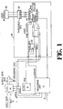
- a digital processing system having a processing unit 10, an input data bus 12, a FIFO buffer 14 having a plurality of storage locations coupled to the processing unit 10, the input data bus 12, and an output data bus 13, a system clock 16, and a threshold detection circuit 18 coupled to the processing unit 10.
- the threshold detection circuit 18 includes a threshold register 20, an Up/Down counter 22, and a pulse generator 24.
- the threshold register 20 has been shown as an element discrete from the processing unit 10, and is loaded directly with a desired threshold value via a user interface 28. It will be understood, however, that the threshold register 20 may constitute one of a number of general purpose registers provided as part of the processing unit 10 that may be loaded via an input bus 11 connected to the processing unit 10.
- the threshold register 20 can also reside within the FIFO buffer 14, in which case the counter 22 would have to be coupled to the output data bus 13 to received the threshold value from the threshold register 20.
- a load threshold value signal (LOADTHR) is supplied to the counter 22 after the threshold value has been loaded in the threshold register 20 in order to transfer the threshold value from the threshold register 20 to the counter 22.
- the LOADTHR signal is generated by the processing unit 10.
- circuitry can be provided within the threshold detection circuit 18 to detect the loading of the threshold value into the threshold register 20 and generate the LOADTHR signal.
- the output of the threshold register 20 is coupled to the input of counter 22 via inverters 26, which results in the one's complement of the value stored in the register 20 being loaded in the counter 22 when a load threshold value signal (LOADTHR) is received by the counter 22.
- the pulse generator 24 of the threshold detection logic 18 also generates a count-up pulse on the falling edge of the LOADTHR signal which increments the counter 22 by one (the counter increments when both the Up/Down and ENABLE inputs are at a logic high level, and decrements when the Up/Down input is at a logic low level and the ENABLE input is high), thereby resulting in the two's complement of the threshold value stored in the threshold register 20 being loaded in the counter 22.
- the digital processing system is then ready to process data received from the data bus 12.
- the FIFO buffer 14 sequentially stores digital data words received from the input data bus 12 in the storage locations, until the processing unit 10 has time to fetch the stored data words from the FIFO buffer 14 by performing a read operation.
- the FIFO buffer 14 contains eight storage locations, the data words can be received and stored in the FIFO buffer 14 at the rate of one data word per clock cycle, and the processing unit requires three clock cycles to perform a read operation from the FIFO after being interrupted from performing a given task.
- the threshold value should be set at a maximum of five, and more preferably at four, in order to insure data overflow does not occur.
- the counter 22 has a counting range one order of magnitude greater than the range of the adjustable threshold value. In other words, the counter has a 2 N+1 counting range if the desired adjustable threshold requires a range of 2 N .
- the counter 22 is a four bit counter, and a range of eight (0-7) is provided for the threshold value by three input bits to the counter 22, with the most significant input bit (MSIB) of the counter 22 being connected to ground.
- MSIB most significant input bit
- the most significant output bit (MSOB) or overflow bit of the counter 22 is used to generate a threshold interrupt signal (THRESHOLD) which is supplied to the processing unit 10.
- the THRESHOLD signal indicates to the processing unit 10 that a read operation must be performed from the FIFO buffer 14 in order to prevent a loss of data from occurring.
- the THRESHOLD interrupt signal it is necessary to generate the THRESHOLD interrupt signal when the number of excess write operations, i.e., the total number of write operations less the total number of read operations, is equal to or greater than the programmed threshold value. Taking the two's complement of the desired threshold value permits the overflow bit of the counter to be used to generate the THRESHOLD signal when the number of excess write operations (W) reaches and exceeds the threshold value as shown in Fig. 2. The overflow bit of the counter will remain high as long as W is equal to or greater than the threshold value.
- the threshold value is set to five (0101)
- the two's complement of five (0011) will be loaded into the counter 22 (note two's complement was not performed on MSIB which was grounded).
- the counter 22 will then increment as follows for excess write operations:
- FIG. 3 A second embodiment of the threshold detection circuit 18' employing only the one's complement is illustrated in Fig. 3.
- the second embodiment does not require the use of a pulse generator to load the two's complement in the counter 22'. Instead, the least significant output bits of the counter 22' are supplied to an AND gate 30, the output of which is supplied to an OR gate 32 along with the overflow bit to generate the THRESHOLD signal.
- the output of the counter 22' will go to 0111 when W equals the threshold value, resulting in the THRESHOLD line going high when the 0111 output of the counter 22' passes through the gates 30 and 32. If additional excess write operations occur, the overflow bit of the counter 22' will go to a logic "1" also causing the THRESHOLD line to go High.
- the threshold detection circuit 18' illustrated in Fig. 3 will also generate the THRESHOLD interrupt when N is equal to or greater than the threshold value.
- the above description is of preferred exemplary embodiments of the present invention, and the invention is not limited to the specific forms shown.
- the threshold detection circuit 18' can be modified as illustrated in Fig. 5 by typing the MSIB of the counter high and inverting the MSOB output of the counter to generate the THRESHOLD interrupt signal when W is less than or equal to the threshold value.
- Other variations and modifications can be made and it is intended to include all such variations and modifications that fall within the scope of the appended claims.
Landscapes
- Engineering & Computer Science (AREA)
- Theoretical Computer Science (AREA)
- Physics & Mathematics (AREA)
- General Physics & Mathematics (AREA)
- General Engineering & Computer Science (AREA)
- Computing Systems (AREA)
- Mathematical Optimization (AREA)
- Mathematical Physics (AREA)
- Pure & Applied Mathematics (AREA)
- Mathematical Analysis (AREA)
- Computational Mathematics (AREA)
- Information Transfer Systems (AREA)
- Manipulation Of Pulses (AREA)
- Communication Control (AREA)
- Executing Machine-Instructions (AREA)
Claims (4)
- Appareil comprenant une mémoire tampon (14) ayant un circuit logique de détection avec seuil, l'appareil comprenant :une mémoire tampon (14) pour stocker des instructions de programme;un moyen d'écriture pour inscrire ces instructions dans ladite mémoire tampon (14);un moyen de lecture pour lire les instructions de ladite mémoire tampon (14);un premier moyen (10) pour charger une valeur de seuil dans un registre de valeur de seuil (20), la valeur de seuil étant liée à la capacité de stockage de la mémoire tampon (14);un second moyen pour charger un zéro binaire dans le bit d'entrée le plus significatif du compteur et une valeur initiale de compte qui est le complément primaire ou le complément secondaire de la valeur de seuil de l'autre bit d'entrée du compteur (22);un moyen d'incrémentation pour incrémenter ledit compteur (22) en réponse à un premier signal fourni en réponse à chaque opération d'écriture réalisé par le moyen d'écriture;un moyen de décrémentation pour décrémenter ledit compteur (22) en réponse à un second signal fourni en réponse à chaque opération de lecture réalisé par le moyen de lecture, etun troisième moyen pour générer un signal de sortie indiquant que la valeur de seuil a été atteinte quand la différence entre le nombre total de premières opérations réalisées par le compteur (22) et le nombre total de secondes opérations réalisées par ledit compteur est supérieure ou égale à la valeur de seuil.
- Appareil selon la revendication 1, dans lequel la valeur de seuil a une étendue de 2N et le compteur a une étendue de compte de 2N+1, où N est un nombre entier égal au nombre de bits du compteur.
- Appareil comprenant une mémoire tampon (14) ayant un circuit logique de détection avec seuil, l'appareil comprenant :une mémoire tampon (14) pour stocker des instructions de programme;un moyen d'écriture pour inscrire ces instructions dans ladite mémoire tampon (14);un moyen de lecture pour lire les instructions de ladite mémoire tampon (14);un compteur (22) ;un premier moyen (10) pour charger une valeur de seuil dans un registre de valeur de seuil (20), la valeur de seuil étant liée à la capacité de stockage de la mémoire tampon (14);un second moyen pour charger un 1 binaire dans le bit d'entrée le plus significatif du compteur et une valeur initiale de compte qui est le complément primaire ou le complément secondaire de la valeur de seuil de l'autre bit d'entrée du compteur (22);un moyen d'incrémentation pour incrémenter ledit compteur (22) en réponse à un premier signal fourni en réponse à chaque opération d'écriture réalisé par le moyen d'écriture;un moyen de décrémentation pour décrémenter ledit compteur (22) en réponse à un second signal fourni en réponse à chaque opération de lecture réalisé par le moyen de lecture, etun troisième moyen pour générer un signal de sortie indiquant que la valeur de seuil a été atteinte quand la différence entre le nombre total de premières opérations réalisées par le compteur (22) et le nombre total de secondes opérations réalisées par ledit compteur est supérieure ou égale à la valeur de seuil.
- Appareil selon la revendication 3, dans lequel la valeur de seuil a une étendue de 2N et le compteur a une étendue de compte de 2N+1, où N est un nombre entier égal au nombre de bits du compteur.
Applications Claiming Priority (2)
| Application Number | Priority Date | Filing Date | Title |
|---|---|---|---|
| US07/343,622 US4969164A (en) | 1989-04-27 | 1989-04-27 | Programmable threshold detection logic for a digital storage buffer |
| US343622 | 1999-06-30 |
Publications (3)
| Publication Number | Publication Date |
|---|---|
| EP0395210A2 EP0395210A2 (fr) | 1990-10-31 |
| EP0395210A3 EP0395210A3 (fr) | 1992-08-05 |
| EP0395210B1 true EP0395210B1 (fr) | 1996-12-18 |
Family
ID=23346862
Family Applications (1)
| Application Number | Title | Priority Date | Filing Date |
|---|---|---|---|
| EP90302685A Expired - Lifetime EP0395210B1 (fr) | 1989-04-27 | 1990-03-14 | Circuit de détection de seuil pour des tampons de stockage numériques |
Country Status (5)
| Country | Link |
|---|---|
| US (1) | US4969164A (fr) |
| EP (1) | EP0395210B1 (fr) |
| JP (1) | JPH02300820A (fr) |
| AT (1) | ATE146610T1 (fr) |
| DE (1) | DE69029422T2 (fr) |
Families Citing this family (22)
| Publication number | Priority date | Publication date | Assignee | Title |
|---|---|---|---|---|
| US5278956A (en) * | 1990-01-22 | 1994-01-11 | Vlsi Technology, Inc. | Variable sized FIFO memory and programmable trigger level therefor for use in a UART or the like |
| JPH07120929B2 (ja) * | 1990-10-29 | 1995-12-20 | 三菱電機株式会社 | パルス発生回路 |
| US5201692A (en) * | 1991-07-09 | 1993-04-13 | Hydro-Gear Limited Partnership | Rider transaxle having hydrostatic transmission |
| DE69124606T2 (de) * | 1991-10-17 | 1997-08-21 | Ibm | Adaptive FIFO-Speichersteuerung |
| EP0574598A1 (fr) * | 1992-06-13 | 1993-12-22 | International Business Machines Corporation | Mémoire tampon de données |
| US5355113A (en) * | 1992-06-22 | 1994-10-11 | Sgs-Thomson Microelectronics, Inc. | Serialized difference flag circuit |
| US5323272A (en) * | 1992-07-01 | 1994-06-21 | Ampex Systems Corporation | Time delay control for serial digital video interface audio receiver buffer |
| US5412782A (en) | 1992-07-02 | 1995-05-02 | 3Com Corporation | Programmed I/O ethernet adapter with early interrupts for accelerating data transfer |
| US5381126A (en) * | 1992-07-31 | 1995-01-10 | Sgs-Thompson Microelectronics, Inc. | Programmable difference flag logic |
| JPH06187178A (ja) * | 1992-12-18 | 1994-07-08 | Hitachi Ltd | 仮想計算機システムの入出力割込み制御方法 |
| EP0685797A1 (fr) * | 1994-06-03 | 1995-12-06 | Hewlett-Packard Company | Circuit de protection de débordement pour un dispositif UART |
| JPH08221311A (ja) * | 1994-12-22 | 1996-08-30 | Sun Microsyst Inc | スーパースカラプロセッサにおけるロードバッファ及びストアバッファの優先順位の動的切換え |
| FR2774784B1 (fr) * | 1998-02-12 | 2004-09-24 | Inside Technologies | Microprocesseur comportant un systeme de synchronisation avec un evenement asynchrone attendu |
| US6327249B1 (en) * | 1999-08-04 | 2001-12-04 | Ess Technology, Inc | Data communication device |
| US20050033942A1 (en) * | 2003-08-08 | 2005-02-10 | Simcha Gochman | Distribution of architectural state information in a processor across multiple pipeline stages |
| US7038499B1 (en) * | 2004-05-27 | 2006-05-02 | National Semiconductor Corporation | System and method for a programmable threshold detector for automatically switching to an active mode or standby mode in a device |
| US7702887B1 (en) * | 2004-06-30 | 2010-04-20 | Sun Microsystems, Inc. | Performance instrumentation in a fine grain multithreaded multicore processor |
| TWI379554B (en) * | 2008-05-21 | 2012-12-11 | Realtek Semiconductor Corp | Data access device and method for communication system |
| US20100115494A1 (en) * | 2008-11-03 | 2010-05-06 | Gorton Jr Richard C | System for dynamic program profiling |
| US8024719B2 (en) | 2008-11-03 | 2011-09-20 | Advanced Micro Devices, Inc. | Bounded hash table sorting in a dynamic program profiling system |
| US8478948B2 (en) | 2008-12-04 | 2013-07-02 | Oracle America, Inc. | Method and system for efficient tracing and profiling of memory accesses during program execution |
| US10706101B2 (en) | 2016-04-14 | 2020-07-07 | Advanced Micro Devices, Inc. | Bucketized hash tables with remap entries |
Family Cites Families (5)
| Publication number | Priority date | Publication date | Assignee | Title |
|---|---|---|---|---|
| GB1485616A (en) * | 1973-04-19 | 1977-09-14 | Post Office | Apparatus for displaying an extreme value among a succession of digital values and method of testing pulse code modulation equipment using such apparatus |
| JPS5291638A (en) * | 1976-01-29 | 1977-08-02 | Sony Corp | D/a converter |
| US4667337A (en) * | 1985-08-28 | 1987-05-19 | Westinghouse Electric Corp. | Integrated circuit having outputs configured for reduced state changes |
| US4713832A (en) * | 1986-04-11 | 1987-12-15 | Ampex Corporation | Programmable divider up/down counter with anti-aliasing feature and asynchronous read/write |
| US4837748A (en) * | 1986-11-13 | 1989-06-06 | Vitelic Corporation | Counting RAM |
-
1989
- 1989-04-27 US US07/343,622 patent/US4969164A/en not_active Expired - Lifetime
-
1990
- 1990-03-14 DE DE69029422T patent/DE69029422T2/de not_active Expired - Fee Related
- 1990-03-14 EP EP90302685A patent/EP0395210B1/fr not_active Expired - Lifetime
- 1990-03-14 AT AT90302685T patent/ATE146610T1/de not_active IP Right Cessation
- 1990-04-26 JP JP2114934A patent/JPH02300820A/ja active Pending
Also Published As
| Publication number | Publication date |
|---|---|
| DE69029422T2 (de) | 1997-07-10 |
| ATE146610T1 (de) | 1997-01-15 |
| US4969164A (en) | 1990-11-06 |
| EP0395210A3 (fr) | 1992-08-05 |
| EP0395210A2 (fr) | 1990-10-31 |
| DE69029422D1 (de) | 1997-01-30 |
| JPH02300820A (ja) | 1990-12-13 |
Similar Documents
| Publication | Publication Date | Title |
|---|---|---|
| EP0395210B1 (fr) | Circuit de détection de seuil pour des tampons de stockage numériques | |
| US5278956A (en) | Variable sized FIFO memory and programmable trigger level therefor for use in a UART or the like | |
| US4486854A (en) | First-in, first-out memory system | |
| US5027330A (en) | FIFO memory arrangement including a memory location fill indication | |
| US4507760A (en) | First-in, first-out (FIFO) memory configuration for queue storage | |
| US5590304A (en) | Circuits, systems and methods for preventing queue overflow in data processing systems | |
| US5384744A (en) | Look ahead flag for FIFO | |
| US4604682A (en) | Buffer system for interfacing an intermittently accessing data processor to an independently clocked communications system | |
| US4803654A (en) | Circular first-in, first out buffer system for generating input and output addresses for read/write memory independently | |
| GB2112533A (en) | Detecting signal sequences | |
| US4151598A (en) | Priority assignment apparatus for use in a memory controller | |
| KR960005106B1 (ko) | 버퍼관리장치 | |
| US6745265B1 (en) | Method and apparatus for generating status flags in a memory device | |
| US5469449A (en) | FIFO buffer system having an error detection and resetting unit | |
| GB1482688A (en) | Storage configuration comprising a main store and a buffer store | |
| US4970679A (en) | Pulse input apparatus | |
| EP0057096A2 (fr) | Unité de traitement d'information | |
| EP0205122A2 (fr) | Prédémultiplicateur de compteur d'évènements | |
| US6480912B1 (en) | Method and apparatus for determining the number of empty memory locations in a FIFO memory device | |
| US5056005A (en) | Data buffer device using first-in first-out memory and data buffer array device | |
| JP2604482B2 (ja) | Fifoレジスタ | |
| EP0364720A1 (fr) | Technique pour exécuter les transferts UART de capacité 8 bits, sur un bus de données 16 bits | |
| US5161217A (en) | Buffered address stack register with parallel input registers and overflow protection | |
| US4771402A (en) | Address comparator | |
| EP0382699A2 (fr) | Système et méthode de transmission de donneés entre processeurs |
Legal Events
| Date | Code | Title | Description |
|---|---|---|---|
| PUAI | Public reference made under article 153(3) epc to a published international application that has entered the european phase |
Free format text: ORIGINAL CODE: 0009012 |
|
| AK | Designated contracting states |
Kind code of ref document: A2 Designated state(s): AT BE CH DE DK ES FR GB GR IT LI LU NL SE |
|
| PUAL | Search report despatched |
Free format text: ORIGINAL CODE: 0009013 |
|
| AK | Designated contracting states |
Kind code of ref document: A3 Designated state(s): AT BE CH DE DK ES FR GB GR IT LI LU NL SE |
|
| 17P | Request for examination filed |
Effective date: 19921030 |
|
| 17Q | First examination report despatched |
Effective date: 19941007 |
|
| GRAG | Despatch of communication of intention to grant |
Free format text: ORIGINAL CODE: EPIDOS AGRA |
|
| GRAH | Despatch of communication of intention to grant a patent |
Free format text: ORIGINAL CODE: EPIDOS IGRA |
|
| GRAH | Despatch of communication of intention to grant a patent |
Free format text: ORIGINAL CODE: EPIDOS IGRA |
|
| GRAA | (expected) grant |
Free format text: ORIGINAL CODE: 0009210 |
|
| RAP1 | Party data changed (applicant data changed or rights of an application transferred) |
Owner name: ADVANCED MICRO DEVICES, INC. |
|
| AK | Designated contracting states |
Kind code of ref document: B1 Designated state(s): AT BE CH DE DK ES FR GB GR IT LI LU NL SE |
|
| PG25 | Lapsed in a contracting state [announced via postgrant information from national office to epo] |
Ref country code: NL Free format text: LAPSE BECAUSE OF FAILURE TO SUBMIT A TRANSLATION OF THE DESCRIPTION OR TO PAY THE FEE WITHIN THE PRESCRIBED TIME-LIMIT Effective date: 19961218 Ref country code: IT Free format text: LAPSE BECAUSE OF FAILURE TO SUBMIT A TRANSLATION OF THE DESCRIPTION OR TO PAY THE FEE WITHIN THE PRE;WARNING: LAPSES OF ITALIAN PATENTS WITH EFFECTIVE DATE BEFORE 2007 MAY HAVE OCCURRED AT ANY TIME BEFORE 2007. THE CORRECT EFFECTIVE DATE MAY BE DIFFERENT FROM THE ONE RECORDED.SCRIBED TIME-LIMIT Effective date: 19961218 Ref country code: LI Effective date: 19961218 Ref country code: DK Effective date: 19961218 Ref country code: AT Effective date: 19961218 Ref country code: CH Effective date: 19961218 Ref country code: BE Effective date: 19961218 Ref country code: ES Free format text: THE PATENT HAS BEEN ANNULLED BY A DECISION OF A NATIONAL AUTHORITY Effective date: 19961218 Ref country code: GR Free format text: LAPSE BECAUSE OF FAILURE TO SUBMIT A TRANSLATION OF THE DESCRIPTION OR TO PAY THE FEE WITHIN THE PRESCRIBED TIME-LIMIT Effective date: 19961218 |
|
| REF | Corresponds to: |
Ref document number: 146610 Country of ref document: AT Date of ref document: 19970115 Kind code of ref document: T |
|
| REF | Corresponds to: |
Ref document number: 69029422 Country of ref document: DE Date of ref document: 19970130 |
|
| PG25 | Lapsed in a contracting state [announced via postgrant information from national office to epo] |
Ref country code: SE Effective date: 19970318 |
|
| ET | Fr: translation filed | ||
| PG25 | Lapsed in a contracting state [announced via postgrant information from national office to epo] |
Ref country code: LU Free format text: LAPSE BECAUSE OF NON-PAYMENT OF DUE FEES Effective date: 19970331 |
|
| NLV1 | Nl: lapsed or annulled due to failure to fulfill the requirements of art. 29p and 29m of the patents act | ||
| REG | Reference to a national code |
Ref country code: CH Ref legal event code: PL |
|
| PLBE | No opposition filed within time limit |
Free format text: ORIGINAL CODE: 0009261 |
|
| STAA | Information on the status of an ep patent application or granted ep patent |
Free format text: STATUS: NO OPPOSITION FILED WITHIN TIME LIMIT |
|
| 26N | No opposition filed | ||
| PGFP | Annual fee paid to national office [announced via postgrant information from national office to epo] |
Ref country code: FR Payment date: 20010301 Year of fee payment: 12 |
|
| PGFP | Annual fee paid to national office [announced via postgrant information from national office to epo] |
Ref country code: DE Payment date: 20010330 Year of fee payment: 12 |
|
| REG | Reference to a national code |
Ref country code: GB Ref legal event code: IF02 |
|
| PG25 | Lapsed in a contracting state [announced via postgrant information from national office to epo] |
Ref country code: DE Free format text: LAPSE BECAUSE OF NON-PAYMENT OF DUE FEES Effective date: 20021001 |
|
| PG25 | Lapsed in a contracting state [announced via postgrant information from national office to epo] |
Ref country code: FR Free format text: LAPSE BECAUSE OF NON-PAYMENT OF DUE FEES Effective date: 20021129 |
|
| REG | Reference to a national code |
Ref country code: FR Ref legal event code: ST |
|
| PGFP | Annual fee paid to national office [announced via postgrant information from national office to epo] |
Ref country code: GB Payment date: 20030204 Year of fee payment: 14 |
|
| PG25 | Lapsed in a contracting state [announced via postgrant information from national office to epo] |
Ref country code: GB Free format text: LAPSE BECAUSE OF NON-PAYMENT OF DUE FEES Effective date: 20040314 |
|
| GBPC | Gb: european patent ceased through non-payment of renewal fee |
Effective date: 20040314 |