EP0395416A2 - Liaison de données pour bus SCSI - Google Patents
Liaison de données pour bus SCSI Download PDFInfo
- Publication number
- EP0395416A2 EP0395416A2 EP19900304548 EP90304548A EP0395416A2 EP 0395416 A2 EP0395416 A2 EP 0395416A2 EP 19900304548 EP19900304548 EP 19900304548 EP 90304548 A EP90304548 A EP 90304548A EP 0395416 A2 EP0395416 A2 EP 0395416A2
- Authority
- EP
- European Patent Office
- Prior art keywords
- data
- transmitting
- memory
- scsi
- data link
- Prior art date
- Legal status (The legal status is an assumption and is not a legal conclusion. Google has not performed a legal analysis and makes no representation as to the accuracy of the status listed.)
- Withdrawn
Links
Images


Classifications
-
- G—PHYSICS
- G06—COMPUTING OR CALCULATING; COUNTING
- G06F—ELECTRIC DIGITAL DATA PROCESSING
- G06F13/00—Interconnection of, or transfer of information or other signals between, memories, input/output devices or central processing units
- G06F13/38—Information transfer, e.g. on bus
- G06F13/40—Bus structure
- G06F13/4004—Coupling between buses
- G06F13/4027—Coupling between buses using bus bridges
- G06F13/4045—Coupling between buses using bus bridges where the bus bridge performs an extender function
Definitions
- the present invention relates to communications links, and more particularly to a Small Computer Systems Interface (SCSI) bus data link for interfacing two computers or a computer and a peripheral at high speed over great distances using SCSI without requiring modification to existing SCSI bus hardware or software.
- SCSI Small Computer Systems Interface
- SCSI Small Computer Systems Interface
- SCSI bus data link to provide high speed communications between computers and peripherals on their respective SCSI buses, which devices are remotely situated from each other, in a transparent manner to an operator.
- the present invention provides an SCSI bus data link for communicating between remote computers and intelligent peripherals that are coupled to their respective SCSI buses.
- the data link mimics the electrical and functional characteristics of the ANSI X3.131-1986 SCSI specification so that the data link appears transparent to operations performed on an SCSI bus.
- Data in the form of device selection and commands generated by an SCSI initiator are received by a data link module that appears like an SCSI target device to the initiator. This data is sent across a high speed serial interface to another data link module that mimics the behavior of the SCSI initiator to select and write the data to the peripheral device that is the true target of the SCSI initiator's commands.
- the data link module has a serial input/output port and a bi-directional SCSI port which are accessed by a microcomputer.
- a direct memory access machine that includes memories and controllers has access to the serial and SCSI ports.
- the microcomputer performs data transfers between SCSI and serial ports using a single byte transfer algorithm, while the direct memory access machine performs block transfers.
- a data transfer protocol returns an acknowledge byte upon validly receiving data.
- FIG. 1 a simple topology for connecting a remote SCSI device 10 to an SCSI bus 12 is shown.
- a host computer 14 together with associated storage devices 16 are all connected to the SCSI bus 12.
- the SCSI bus 12 is coupled to a data link module 18.
- the data link module 18 communicates with a remote data link module 18′ over a serial data line 20.
- the remote device 10 is coupled to the remote data link module by an extension 12′ of the SCSI bus 12.
- the remote storage device 10 "sees" the SCSI bus 12 as though the data link modules 18, 18′ and serial data line 20 did not exist.
- the host computer 14 "sees" the remote device 10 as being connected to the SCSI bus 12.
- FIG. 2 A more complex single bus topology is shown in Fig. 2 where up to eight devices 14/16 are connected to respective SCSI buses 12 distributed at four remote sites 22. Each remote site 22 is linked to each of the other sites via data link modules 18 and serial data lines 20, a separate data link module at one site being assigned to communicate with each other remote site. Just as in the single peripheral case, communications from one site 22 to another present a transparent operation for the SCSI bus between devices 14/16 situated at different sites. For more than eight devices 14/16, such as the fourteen devices shown in Fig. 3, the connection between sites is the same as for Fig. 2, i.e., one data link module 18 at each site 22 for each other site to which that site is connected.
- the data link module 18 for the remote site 22 is first addressed, and then the desired device at the remote site is addressed.
- This topology using special software, behaves as a connection bridge between two SCSI buses 12 and allows multiple simultaneous transfers between buses.
- Device selection and commands generated by an SCSI initiator at the originating site 22 are received by the appropriate data link module 18 that mimics the behavior of the selected, or target, device 14/16. This data is sent across the serial interface to the data link module 18 at the designated site 22.
- the receiving data link module 18 mimics the SCSI initiator at the originating site to select and write the data to the selected device 14/16 that is the true target of the SCSI initiator's commands. If the command is a request for a data transfer between the initiator and the target, the data link performs this operation at rates matching or exceeding those contained in the SCSI ANSI specification.
- the data transfer protocols across the SCSI bus 12 are defined in the ANSI specification.
- the data transfer protocols across the serial port are governed by the data link modules, and are one of two categories: single byte transfers or block transfers.
- Single byte transfers are performed by transferring bytes of data across the serial port using a double transmit/double acknowledge protocol. This protocol requires that a byte be sent twice across the serial port by the transmitting data link module 18.
- the receiving data link module 18′ compares the received bytes and, if the bytes match, transmits two acknowledge (ACK) bytes back to the transmitting data link module. If the bytes do not match, then a pair of not acknowledged (NACK) bytes are sent to the transmitting data link module 18.
- ACK acknowledge
- NACK not acknowledged
- the transmitting data link module need only receive one of the ACK or NACK bytes to either verify the transfer or attempt a retransmit. If both ACK/NACK bytes are corrupted, the transmitting data link module enters an error recovery state and interrupts the receiving data link module to determine whether an ACK or NACK was transmitted by the receiving data link module before continuing with another transfer.
- Single byte transfers are performed during SCSI arbitration, select, command, end status and reset phases as well as for SCSI data phase transfers for functions that do not use block transfers. Data link module status exchange between data link modules 18 also is performed on a single byte basis.
- Block transfers transfer blocks of data across the serial port using a block checksum/double acknowledge protocol.
- n+1 bytes are transmitted where the n+1th byte is a bit-column exclusive-or (XOR) checksum of the block.
- the checksum is calculated on the fly as the data is being transmitted.
- an XOR checksum also is calculated on the fly as the data is received. Receipt of the n+1th byte triggers a checksum comparison.
- a checksum match generates a double ACK transmission to the transmitting data link module 18, whereas a mismatch transmits a double NACK. If the NACK is received by the transmitting data link module 18, the block is retransmitted until an ACK is received.
- the hardware is designed to match or exceed the maximum SCSI bus data block transfer rates across the serial port, to detect and recover from most serial port bit errors in a parsimonious fashion, and to communicate with an intelligent, i.e., programmable, device across both the SCSI and serial ports.
- the data rate requirement results in a fairly high data rate across the serial port. Assuming eight bits of SCSI data with a parity bit and a special data link status bit, a four megabyte per second SCSI block transfer demands a minimum serial port data rate of forty megabits per second. To support block retransmits due to detected errors, sufficient memory space is required to hold the data after the initial transmission while allowing overlapped transfers across the SCSI bus.
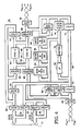
- the basic hardware architecture for a data link module 18 shown in Fig. 4 is designed to meet these functional criteria.
- a receiver 24 and a transmitter 26 form a serial port interface. Outgoing/incoming serial data is routed to/from the receiver/transmitter from either an optical or electrical transmitter/receiver (not shown).
- An SCSI port provides bi-directional access to the SCSI data and status lines that make up the SCSI bus 12 by means of a pair of transceivers 28, 30 and latches 32, 34, 36.
- a microprocessor 38 accesses both the serial and SCSI ports via a first bus 40.
- a high speed direct memory access (DMA) machine composed of a microcontroller 42, SCSI & FIFO controller 44 and first-in, first-out (FIFO) memories 46, 48, also accesses the SCSI and serial ports via data buses 50, 52, 54.
- DMA direct memory access
- a RCVR CLKS & FIFO WR device 56 and a XMTR CLKS & FIFO RD device 58 are programmable devices that manage serial port traffic to the microcomputer 38 and the DMA machine.
- Block data from the receiver 24 is input to one of the memories 46, 48 via a buffer 60.
- block data from the SCSI bus is loaded into the memories 46, 48 via an SCSI buffer 62.
- the block data in the memories 46, 48 is either output to the SCSI port via latch 64 over data bus 54 or to the serial port via buffer 66 to the transmitter 26.
- a checksum comparator 68 calculates the checksum for the block transfer from the serial port on the fly and compares that number with the checksum byte of the block data.
- a checksum generator 70 calculates the checksum to be added as the n+1th byte of the block transfer to the serial port for transmission. For single byte transfers the received duplicate bytes from the serial port are received by the microprocessor 38 via a receive latch 72, while transmitted bytes are output by the microprocessor via a transmit latch 74 to the serial port. The single bytes are output onto or input from the SCSI port by the microprocessor 38 via the transceiver 30.
- the checksum comparison or byte comparison for the received data causes a link ACK/NACK block 76 to output the appropriate acknowledgment to the serial port to indicate to the transmitting data link module 18 whether the data transfer occurred with or without error. Incoming ACK/NACK is recognized and signalled by the link status 78.
- the SCSI & FIFO controller 44 has a byte counter, a block counter and several programmable logic devices (PLD).
- the byte counter keeps track of the number of bytes in a block
- the block counter keeps track of the number of blocks in a transfer. Both counters are loaded at the beginning of a transfer by the microprocessor 38.
- the PLDs generate read and write strobes for the appropriate memories 46, 48 from the SCSI port as well as SCSI bus request and acknowledge signals.
- the controller 42 determines which memory 46, 48 is being written/read by the SCSI bus 12 as opposed to read/written by the serial port, and steers the appropriate control signals to the SCSI & FIFO controller 44, the RCVR CLKS & FIFO WR 56 and the XMTR CLKS & FIFO RD 58 PLDs.
- the checksums are generated on the fly and sent automatically by the XMTR CLKS & FIFO RD 58 PLD.
- the output of the checksum comparator 68 is tested after receipt of the n+1th byte. If the comparison is true, an ACK is sent by the controller 42 from the link ACK/NACK block 76.
- the controller 42 tests the output of a link status register 78 for either ACK or NACK. If the result is an ACK and there is an unsent block of data in one of the memories 46, 48, the unsent data is readied for transmission across the link. If an additional block is to be received from the SCSI port, the empty memory 46, 48 has this new data block written into it. At the receiving data link module 18′ the now loaded memory 46, 48 is read by the SCSI port and the previously emptied memory 48, 46 is readied for serial port write.
- the controller 42 If during the receipt of a block transfer the output of the checksum comparator 68 is false, the controller 42 resets the receiving memory 46, 48 write pointer, sends a NACK from the link ACK/NACK block 76 to the transmitting data link module 18, and notifies the microprocessor 38 that a bad block was received. The microprocessor 38 notes this condition and returns control back to the controller 42. At the transmitting data link module receipt of the NACK by the link status register 78 is indicated to the microprocessor by the controller 42. This is noted and control returned to the controller 42. The transmitting memory's read pointer is reset and the transfer is reattempted.
- Bridging separate SCSI buses 12 together as in Fig. 3 requires a few modifications to the basic data link operation.
- the data link modules 18 are assigned an SCSI bus address so that the onboard microprocessor 38 only responds to bus activity addressed to it.
- Second a Bridge to Remote Bus SCSI function is issued to the selected data link module. This function contains all the parameters of a normal block or non-block SCSI command. These parameters are sent across the link to the receiving data link module 18, where a normal SCSI access is performed to the targeted device 14/16.
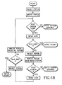
- the data link modules 18 involved are initialized and a determination is made as to whether the particular data link module is transmitting from the SCSI port to the serial port or is receiving from the serial port to the SCSI port. If the data link module is receiving data from the SCSI port a write routine is accessed, otherwise if transmitting to the SCSI port a read routine is accessed.
- the read routine (Fig. 5b) resets FIFO A 46 and then writes the data from the serial port into FIFO A.
- the output of the checksum comparator 68 is tested to see if the checksum from the data matches that calculated on the fly. If the checksums match, an ACK byte is sent to the transmitting data link module. If there are no more blocks of data to be received, then the routine returns to start. Otherwise the next FIFO B 48 is prepared to receive the next block of data.
- data in FIFO A is read by the SCSI port. Again the checksum is tested for a match, and if true the ACK byte is transmitted and FIFO A is prepared to receive the next block of data, if there is any.
- a checksum error routine (Fig. 5e) resets that FIFO, signals to the microprocessor 38 that there is a checksum error and sends a NACK byte to the transmitting data link module. The retransmitted data is then read into the same FIFO and the checksum is tested again. If there is still a checksum error, the routine is recycled, otherwise the routine returns to the read routine at the point after the checksum test for that FIFO.
- the write routine (Fig. 5c) is accessed.
- the first memory FIFO A 46 is initialized and data from the SCSI port is written into FIFO A.
- the second memory FIFO B 48 is then initialized and a test is made regarding whether there are any more blocks of data to send. If there are more blocks to send, the data is written from the SCSI port into FIFO B while the data in FIFO A is read out to the serial port. After the data is read out to the serial port from FIFO A, a test is made to determine whether an ACK byte has been received from the receiving data link module.
- ACK is received, then the cycle is repeated by resetting FIFO A, testing for the end of blocks of data, and then reading out the data from FIFO B to the serial port while writing in data from the SCSI bus to the FIFO A.
- a write end routine (Fig. 5f) is accessed.
- the write end routine reads the FIFO for transmission of the data via the serial port.
- the controller 42 signals the microprocessor 38 that the block transfer is complete and returns to the starting conditions.
- a link error routine (Fig. 5d) is accessed.
- the link error routine resets the read pointer for the memory, signals a link error to the microprocessor 38, and then rereads the data out to the serial port. If NACK is received, the routine is repeated, otherwise the routine returns to the write routine at the point after the ACK test that generated the initial error.
- the present invention provides an SCSI bus data link for communicating transparently between remote devices connected to an SCSI bus.
- a data link module connected to the SCSI bus has an SCSI port for transferring data between the SCSI bus and the module and a serial port for transferring data between modules over a serial data line.
- the data link module appears to the SCSI initiator as an SCSI target device, while it appears to an SCSI target device as an SCSI initiator.
Landscapes
- Engineering & Computer Science (AREA)
- General Engineering & Computer Science (AREA)
- Theoretical Computer Science (AREA)
- Computer Hardware Design (AREA)
- Physics & Mathematics (AREA)
- General Physics & Mathematics (AREA)
- Communication Control (AREA)
- Information Transfer Systems (AREA)
- Computer And Data Communications (AREA)
Applications Claiming Priority (2)
| Application Number | Priority Date | Filing Date | Title |
|---|---|---|---|
| US343990 | 1982-01-29 | ||
| US34399089A | 1989-04-26 | 1989-04-26 |
Publications (1)
| Publication Number | Publication Date |
|---|---|
| EP0395416A2 true EP0395416A2 (fr) | 1990-10-31 |
Family
ID=23348549
Family Applications (1)
| Application Number | Title | Priority Date | Filing Date |
|---|---|---|---|
| EP19900304548 Withdrawn EP0395416A2 (fr) | 1989-04-26 | 1990-04-26 | Liaison de données pour bus SCSI |
Country Status (2)
| Country | Link |
|---|---|
| EP (1) | EP0395416A2 (fr) |
| JP (1) | JPH034351A (fr) |
Cited By (19)
| Publication number | Priority date | Publication date | Assignee | Title |
|---|---|---|---|---|
| EP0549217A1 (fr) * | 1991-12-20 | 1993-06-30 | International Business Machines Corporation | Interface SCSI pour dispositifs SCSI non-locaux |
| FR2698464A1 (fr) * | 1992-11-24 | 1994-05-27 | Bull Sa | Système d'appareils distribués en réseau. |
| EP0520838A3 (en) * | 1991-06-28 | 1994-08-24 | Digital Equipment Corp | Scsi interface employing bus extender and auxiliary bus |
| WO1996003695A1 (fr) * | 1994-07-22 | 1996-02-08 | Siemens Nixdorf Informationssysteme Ag | Reduction de donnees pour coupleurs de bus |
| WO1996025708A1 (fr) * | 1995-02-13 | 1996-08-22 | Essnet Ab | Appareil de transmission serielle de donnees |
| GB2308904A (en) * | 1996-01-06 | 1997-07-09 | Earl Walter Roper | SCSI bus extension over the ethernet |
| EP0542087A3 (fr) * | 1991-11-10 | 1997-12-29 | Hewlett-Packard Company | Méthode et appareil pour transmission en série efficace des signaux de commande dans un bus numérique |
| EP0844567A1 (fr) * | 1996-11-21 | 1998-05-27 | Hewlett-Packard Company | Passerelle de PCI-bus à grande distance |
| EP0910021A1 (fr) * | 1997-10-16 | 1999-04-21 | Alcatel | Dispositif de communication entre plusieurs processeurs |
| EP0672274A4 (fr) * | 1992-12-02 | 2000-11-22 | Sand Technology Systems Int | Extension de reseau informatique |
| WO2001044959A1 (fr) * | 1999-12-15 | 2001-06-21 | Robotel Electronique Inc. | Extension de bus peripherique |
| EP1133732A4 (fr) * | 1998-10-30 | 2003-01-22 | Cybex Computer Prod Corp | Architecture d'ordinateur fractionnee |
| US6748473B1 (en) | 1998-10-30 | 2004-06-08 | Avocent Huntsville Corporation | Split computer system including transmission of video data between plural enclosures |
| US6807639B2 (en) | 1998-10-30 | 2004-10-19 | Avocent Corporation | Split computer architecture to separate user and processor while retaining original user interface |
| US7783820B2 (en) | 2005-12-30 | 2010-08-24 | Avocent Corporation | Packet-switched split computer having disassociated peripheral controller and plural data buses |
| US8385429B2 (en) | 2002-10-01 | 2013-02-26 | Avocent Corporation | Video compression encoder |
| US8660194B2 (en) | 2006-04-28 | 2014-02-25 | Avocent Corporation | DVC delta commands |
| US8805096B2 (en) | 2004-06-25 | 2014-08-12 | Avocent Corporation | Video compression noise immunity |
| US9560371B2 (en) | 2003-07-30 | 2017-01-31 | Avocent Corporation | Video compression system |
Families Citing this family (2)
| Publication number | Priority date | Publication date | Assignee | Title |
|---|---|---|---|---|
| JP2531903B2 (ja) * | 1992-06-22 | 1996-09-04 | インターナショナル・ビジネス・マシーンズ・コーポレイション | コンピュ―タ・システムおよびシステム拡張装置 |
| JPH0690695B2 (ja) * | 1992-06-24 | 1994-11-14 | インターナショナル・ビジネス・マシーンズ・コーポレイション | コンピュータ・システムおよびシステム拡張装置 |
-
1990
- 1990-04-10 JP JP2094926A patent/JPH034351A/ja active Pending
- 1990-04-26 EP EP19900304548 patent/EP0395416A2/fr not_active Withdrawn
Cited By (29)
| Publication number | Priority date | Publication date | Assignee | Title |
|---|---|---|---|---|
| EP0520838A3 (en) * | 1991-06-28 | 1994-08-24 | Digital Equipment Corp | Scsi interface employing bus extender and auxiliary bus |
| EP0542087A3 (fr) * | 1991-11-10 | 1997-12-29 | Hewlett-Packard Company | Méthode et appareil pour transmission en série efficace des signaux de commande dans un bus numérique |
| EP0549217A1 (fr) * | 1991-12-20 | 1993-06-30 | International Business Machines Corporation | Interface SCSI pour dispositifs SCSI non-locaux |
| US5499378A (en) * | 1991-12-20 | 1996-03-12 | International Business Machines Corporation | Small computer system emulator for non-local SCSI devices |
| FR2698464A1 (fr) * | 1992-11-24 | 1994-05-27 | Bull Sa | Système d'appareils distribués en réseau. |
| EP0599705A1 (fr) * | 1992-11-24 | 1994-06-01 | Bull S.A. | Système d'appareils distribués en réseau |
| CN1036949C (zh) * | 1992-11-24 | 1998-01-07 | 布尔有限公司 | 分布在网络中的单元的系统 |
| EP0672274A4 (fr) * | 1992-12-02 | 2000-11-22 | Sand Technology Systems Int | Extension de reseau informatique |
| WO1996003695A1 (fr) * | 1994-07-22 | 1996-02-08 | Siemens Nixdorf Informationssysteme Ag | Reduction de donnees pour coupleurs de bus |
| US5878236A (en) * | 1994-07-22 | 1999-03-02 | Siemens Nixdorf Informationssysteme Aktiengesellschaft | Method for coupling segments of a bus system |
| WO1996025708A1 (fr) * | 1995-02-13 | 1996-08-22 | Essnet Ab | Appareil de transmission serielle de donnees |
| GB2308904A (en) * | 1996-01-06 | 1997-07-09 | Earl Walter Roper | SCSI bus extension over the ethernet |
| US6003105A (en) * | 1996-11-21 | 1999-12-14 | Hewlett-Packard Company | Long-haul PCI-to-PCI bridge |
| EP0844567A1 (fr) * | 1996-11-21 | 1998-05-27 | Hewlett-Packard Company | Passerelle de PCI-bus à grande distance |
| FR2770008A1 (fr) * | 1997-10-16 | 1999-04-23 | Alsthom Cge Alcatel | Dispositif de communication entre plusieurs processeurs |
| EP0910021A1 (fr) * | 1997-10-16 | 1999-04-21 | Alcatel | Dispositif de communication entre plusieurs processeurs |
| US7020732B2 (en) | 1998-10-30 | 2006-03-28 | Avocent Huntsville Corporation | Split computer architecture |
| EP1133732A4 (fr) * | 1998-10-30 | 2003-01-22 | Cybex Computer Prod Corp | Architecture d'ordinateur fractionnee |
| US6748473B1 (en) | 1998-10-30 | 2004-06-08 | Avocent Huntsville Corporation | Split computer system including transmission of video data between plural enclosures |
| US6807639B2 (en) | 1998-10-30 | 2004-10-19 | Avocent Corporation | Split computer architecture to separate user and processor while retaining original user interface |
| US7320043B2 (en) | 1998-10-30 | 2008-01-15 | Avocent Huntsville Corporation | Split computer architecture to separate user and processor while retaining original user interface |
| US6526468B1 (en) | 1999-12-15 | 2003-02-25 | Robotel Electronique Inc. | Peripheral bus extender |
| WO2001044959A1 (fr) * | 1999-12-15 | 2001-06-21 | Robotel Electronique Inc. | Extension de bus peripherique |
| US8385429B2 (en) | 2002-10-01 | 2013-02-26 | Avocent Corporation | Video compression encoder |
| US9743095B2 (en) | 2002-10-01 | 2017-08-22 | Avocent Corporation | Video compression encoder |
| US9560371B2 (en) | 2003-07-30 | 2017-01-31 | Avocent Corporation | Video compression system |
| US8805096B2 (en) | 2004-06-25 | 2014-08-12 | Avocent Corporation | Video compression noise immunity |
| US7783820B2 (en) | 2005-12-30 | 2010-08-24 | Avocent Corporation | Packet-switched split computer having disassociated peripheral controller and plural data buses |
| US8660194B2 (en) | 2006-04-28 | 2014-02-25 | Avocent Corporation | DVC delta commands |
Also Published As
| Publication number | Publication date |
|---|---|
| JPH034351A (ja) | 1991-01-10 |
Similar Documents
| Publication | Publication Date | Title |
|---|---|---|
| EP0395416A2 (fr) | Liaison de données pour bus SCSI | |
| US6418504B2 (en) | System and method for coupling peripheral buses through a serial bus using a split bridge implementation | |
| KR100290943B1 (ko) | 유니버설 시리얼 버스 제어 이전을 처리하는 장치 및 방법 | |
| US6397273B2 (en) | System having an enhanced parity mechanism in a data assembler/disassembler for use in a pipeline of a host-storage system interface to global memory | |
| US6185631B1 (en) | Program for transferring execution of certain channel functions to a control unit and having means for combining certain commands and data packets in one sequence | |
| US6317805B1 (en) | Data transfer interface having protocol conversion device and upper, lower, middle machines: with middle machine arbitrating among lower machine side requesters including selective assembly/disassembly requests | |
| US6941396B1 (en) | Storage controller redundancy using bi-directional reflective memory channel | |
| US5664223A (en) | System for independently transferring data using two independently controlled DMA engines coupled between a FIFO buffer and two separate buses respectively | |
| KR100290944B1 (ko) | 복합 유니버설 시리얼 버스 제어기에 인터페이스를 제공하기 위한 장치 및 방법 | |
| US7574540B2 (en) | Managing management controller communications | |
| US5619646A (en) | Method and system for dynamically appending a data block to a variable length transmit list while transmitting another data block over a serial bus | |
| AU617446B2 (en) | Improved parity checking apparatus | |
| US6240446B1 (en) | Multiplexing of multiple data packets for multiple input/output operations between multiple input/output devices and a channel subsystem having multiple channels | |
| US7010575B1 (en) | Data storage system having separate data transfer section and message network having bus arbitration | |
| EP0326696A2 (fr) | Adaptateur hybride de liaison de transmission à technologie d'entrée/sortie et de transmission de données | |
| US6651130B1 (en) | Data storage system having separate data transfer section and message network with bus arbitration | |
| EP0676700A1 (fr) | Méthode et dispositif pour la gestion de FIFO's de paquets | |
| JPH07282025A (ja) | クロック回路 | |
| US5574865A (en) | System for data transfer protection during module connection/disconnection onto live bus | |
| US7117275B1 (en) | Data storage system having separate data transfer section and message network | |
| US6609164B1 (en) | Data storage system having separate data transfer section and message network with data pipe DMA | |
| US20090003228A1 (en) | Bad data packet capture device | |
| US6993621B1 (en) | Data storage system having separate data transfer section and message network with plural directors on a common printed circuit board and redundant switching networks | |
| US6631433B1 (en) | Bus arbiter for a data storage system | |
| US6901468B1 (en) | Data storage system having separate data transfer section and message network having bus arbitration |
Legal Events
| Date | Code | Title | Description |
|---|---|---|---|
| PUAI | Public reference made under article 153(3) epc to a published international application that has entered the european phase |
Free format text: ORIGINAL CODE: 0009012 |
|
| AK | Designated contracting states |
Kind code of ref document: A2 Designated state(s): DE FR GB NL |
|
| STAA | Information on the status of an ep patent application or granted ep patent |
Free format text: STATUS: THE APPLICATION HAS BEEN WITHDRAWN |
|
| 18W | Application withdrawn |
Withdrawal date: 19901127 |
|
| R18W | Application withdrawn (corrected) |
Effective date: 19901127 |
|
| R18W | Application withdrawn (corrected) |
Effective date: 19901127 |