EP0401238B1 - Systeme de commutation de communications - Google Patents
Systeme de commutation de communications Download PDFInfo
- Publication number
- EP0401238B1 EP0401238B1 EP89902206A EP89902206A EP0401238B1 EP 0401238 B1 EP0401238 B1 EP 0401238B1 EP 89902206 A EP89902206 A EP 89902206A EP 89902206 A EP89902206 A EP 89902206A EP 0401238 B1 EP0401238 B1 EP 0401238B1
- Authority
- EP
- European Patent Office
- Prior art keywords
- atm
- stm
- cell
- cells
- input
- Prior art date
- Legal status (The legal status is an assumption and is not a legal conclusion. Google has not performed a legal analysis and makes no representation as to the accuracy of the status listed.)
- Expired - Lifetime
Links
- 230000001360 synchronised effect Effects 0.000 claims abstract description 10
- 238000005070 sampling Methods 0.000 claims abstract description 7
- 230000005540 biological transmission Effects 0.000 abstract description 2
- 239000000284 extract Substances 0.000 description 2
- 238000000605 extraction Methods 0.000 description 2
- 238000010586 diagram Methods 0.000 description 1
Images
Classifications
-
- H—ELECTRICITY
- H04—ELECTRIC COMMUNICATION TECHNIQUE
- H04J—MULTIPLEX COMMUNICATION
- H04J3/00—Time-division multiplex systems
- H04J3/16—Time-division multiplex systems in which the time allocation to individual channels within a transmission cycle is variable, e.g. to accommodate varying complexity of signals, to vary number of channels transmitted
-
- H—ELECTRICITY
- H04—ELECTRIC COMMUNICATION TECHNIQUE
- H04L—TRANSMISSION OF DIGITAL INFORMATION, e.g. TELEGRAPHIC COMMUNICATION
- H04L12/00—Data switching networks
- H04L12/54—Store-and-forward switching systems
- H04L12/56—Packet switching systems
- H04L12/5601—Transfer mode dependent, e.g. ATM
-
- H—ELECTRICITY
- H04—ELECTRIC COMMUNICATION TECHNIQUE
- H04J—MULTIPLEX COMMUNICATION
- H04J3/00—Time-division multiplex systems
- H04J3/16—Time-division multiplex systems in which the time allocation to individual channels within a transmission cycle is variable, e.g. to accommodate varying complexity of signals, to vary number of channels transmitted
- H04J3/1682—Allocation of channels according to the instantaneous demands of the users, e.g. concentrated multiplexers, statistical multiplexers
-
- H—ELECTRICITY
- H04—ELECTRIC COMMUNICATION TECHNIQUE
- H04L—TRANSMISSION OF DIGITAL INFORMATION, e.g. TELEGRAPHIC COMMUNICATION
- H04L12/00—Data switching networks
- H04L12/64—Hybrid switching systems
- H04L12/6418—Hybrid transport
-
- H—ELECTRICITY
- H04—ELECTRIC COMMUNICATION TECHNIQUE
- H04L—TRANSMISSION OF DIGITAL INFORMATION, e.g. TELEGRAPHIC COMMUNICATION
- H04L49/00—Packet switching elements
- H04L49/10—Packet switching elements characterised by the switching fabric construction
- H04L49/104—Asynchronous transfer mode [ATM] switching fabrics
-
- H—ELECTRICITY
- H04—ELECTRIC COMMUNICATION TECHNIQUE
- H04L—TRANSMISSION OF DIGITAL INFORMATION, e.g. TELEGRAPHIC COMMUNICATION
- H04L49/00—Packet switching elements
- H04L49/60—Software-defined switches
- H04L49/606—Hybrid ATM switches, e.g. ATM&STM, ATM&Frame Relay or ATM&IP
-
- H—ELECTRICITY
- H04—ELECTRIC COMMUNICATION TECHNIQUE
- H04J—MULTIPLEX COMMUNICATION
- H04J2203/00—Aspects of optical multiplex systems other than those covered by H04J14/05 and H04J14/07
- H04J2203/0001—Provisions for broadband connections in integrated services digital network using frames of the Optical Transport Network [OTN] or using synchronous transfer mode [STM], e.g. SONET, SDH
- H04J2203/0003—Switching fabrics, e.g. transport network, control network
-
- H—ELECTRICITY
- H04—ELECTRIC COMMUNICATION TECHNIQUE
- H04J—MULTIPLEX COMMUNICATION
- H04J2203/00—Aspects of optical multiplex systems other than those covered by H04J14/05 and H04J14/07
- H04J2203/0001—Provisions for broadband connections in integrated services digital network using frames of the Optical Transport Network [OTN] or using synchronous transfer mode [STM], e.g. SONET, SDH
- H04J2203/0089—Multiplexing, e.g. coding, scrambling, SONET
-
- H—ELECTRICITY
- H04—ELECTRIC COMMUNICATION TECHNIQUE
- H04L—TRANSMISSION OF DIGITAL INFORMATION, e.g. TELEGRAPHIC COMMUNICATION
- H04L12/00—Data switching networks
- H04L12/54—Store-and-forward switching systems
- H04L12/56—Packet switching systems
- H04L12/5601—Transfer mode dependent, e.g. ATM
- H04L2012/5672—Multiplexing, e.g. coding, scrambling
-
- H—ELECTRICITY
- H04—ELECTRIC COMMUNICATION TECHNIQUE
- H04L—TRANSMISSION OF DIGITAL INFORMATION, e.g. TELEGRAPHIC COMMUNICATION
- H04L12/00—Data switching networks
- H04L12/64—Hybrid switching systems
- H04L12/6418—Hybrid transport
- H04L2012/6445—Admission control
- H04L2012/6459—Multiplexing, e.g. TDMA, CDMA
Definitions
- the present invention relates to a communication switching system including at least a multiplexer having first and second input terminals to which a first input cell stream and a second input cell stream are applied respectively, said first and second cell streams comprising first and second cells occupying predetermined and arbitrary time slots of respective first and second time frames having a first and a second time slot frequency respectively, and which provides at its output terminal an output cell stream wherein said first and second cells occupy predetermined and arbitrary time slots respectively of a third time frame having a third time slot frequency, each of said cells comprising data, said system additionally including a demultiplexer having an input terminal to which said output cell stream is applied and first and second output terminals to which a first switching exchange for processing said first cell stream and a second switching exchange for processing said second cell stream are connected respectively.
- Such a communication switching system is described in European Patent publication EP-A-0250160, and also in the European Patent Application No 88120438.2 with publication No EP-A-0320772 and published on June 21, 1989.
- the multiplexer inserts the second or ATM (Asynchronous Transfer Mode) cells of the second input cell stream in free time slots of the first input cell stream comprising first or STM (Synchronous Transfer Mode) cells the resultant cell stream being the output cell stream.
- ATM Asynchronous Transfer Mode
- STM Synchronous Transfer Mode
- An object of the present invention is to provide a communication switching system of the above type, but making use of a multiplexer which is particularly advantageous from an economic point of view and may also be used for when all cell streams are ATM cell streams.
- said system includes a transmitter adapted to generate said first and second input cell streams in respective time frames which are phase synchronous with respect to each other, said third frequency being at least equal to the sum of said first and second frequencies, and that said multiplexer is constituted by a switching element comprising a common switching means to which said input and output terminals are coupled via respective receiver and transmitter circuits and which samples said input cell streams in a predetermined order and at said third frequency and supplies the resultant cell stream having said third time frame to said transmitter circuit(s).
- the invention is based on the insight that the switching element disclosed in the PCT application published under No WO87/04579, though it is used therein for the switching of ATM input cell streams, can be used as a multiplexer of ATM and STM input cell streams. Indeed, when the time frames of the input and output cell streams are phase synchronous and when also the above frequency relation is satisfied the sampling of the input cell streams in a predetermined order produces an output cell stream wherein the order of the STM and ATM cells is respected and wherein the STM cells still occupy predetermined time slots. Moreover, this multiplexer may be used irrespective of the synchronous or asynchronous nature of these streams.
- Another characteristic feature of the present communication switching system is that said resultant cell stream obtained by sampling is supplied to a single said transmitter circuit which provides said output cell stream at its said output.
- said demultiplexer is constituted by a switching element comprising a common switching means to which the input terminal and the first and second output terminals of said demultiplexer are coupled via respective receiver and transmitter circuits and which samples said output cell stream at said third frequency and supplies the resultant cell stream, having said third time frame, to said transmitter circuits wherein each of the cells is entered depending on the cell belonging to said first or second cell streams respectively, as indicated in a header of these cells.
- said second switching exchange is built up by means of switching elements of the same structure as those used in said multiplexer and demultiplexer circuits.
- the above second switching exchange can be based on a single type switching element but the latter can also be used in the above multiplexer and demultiplexer circuits, thus ensuring large scale standardisation.
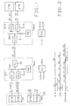
- the communication switching system shown in Fig. 1 includes a plurality of user stations, such as US, including a transmitter TR and a receiver REC which are each coupled to a communication switching exchange STME operating in the STM or Synchronous Transfer Mode, as well as to a communication switching exchange ATME working in the ATM or Asynchronous Transfer Mode.
- the switching exchange STME is for instance a narrow band ISDN exchange of the type described in the article "System 12. ISDN Field Trials in the Belgian, Italian and Spanish Networks" by F. Haerens et al, Electrical Communication, Volume 59, Number 1/2, 1985, pp. 89-97.
- the exchange ATME is e.g. of the type disclosed in the above mentioned PCT application.
- the transmitter TR includes a circuit STMC which is able to generate an STM stream of cells of bits. This means that the cells of this stream which are called STM cells occupy predetermined time slots of a time frame with time slot frequency f2.
- the transmitter TR also includes a circuit ATMC which is able to generate an ATM cell stream of bits. In such a cell stream the cells which are called ATM cells occupy arbitrary time slots of a time frame with time slot frequency f3.
- the cells of the STM and ATM cell streams each have a header containing an indication that an STM or an ATM cell is concerned, i.e. directed to the destination switching exchange STME or ATME.
- the output terminals 01 and 02 of the circuits STMC and ATMC are connected to respective input terminals I1 and I2 of a multiplexer MUX having an output terminal 03.
- the latter is coupled via a transmission link L1 to the input terminal I3 of a demultiplexer DMUX having output terminals 04 and 05 which are connected to input terminals I4 and I5 of the switching exchanges STME and ATME respectively.
- a switching element comprises a common switching means which is constituted by a TDM (Time Division Multiplex) bus and an associated timing circuit, and has a plurality of input and output terminals coupled to the common switching means via respective receiver and transmitter circuits.
- Each such receiver circuit includes the cascade connection of a time frame clock extraction circuit and an input queue wherein the cells of an input cell stream are entered under the control of the clock extracted therefrom by the clock extraction circuit.
- the output portion of the input queue is controlled by the common switching means which operates at a predetermined time slot frequency of an output time frame equal to the sum of the time slot frequencies of the input time frames of the input cell streams fed to the receiver circuits.
- the common switching means checks, in a predetermined order, the presence of complete cells in all the input queues and enters these cells in respective time slots of the output time frame having the above mentioned predetermined frequency. In other words, the common switching means samples the input cell streams at the predetermined time slot frequency. It then supplies the resultant cell stream to the transmitter circuits which enter the cells in function of their header and output these cells, possibly at another time slot frequency.
- the switching element included in the multiplexer MUX is of the above type but has only two input terminals I1, I2 and one output terminal 03 and comprises a timing circuit TM1 which is connected to a common switching bus SB1 to which the terminals I1, I2 and 03 are connected via respective receiver and transmitter circuits RC1, RC2 and TC1.
- the receiver circuits RC1 and RC2 extract the time slot frequencies f2 and f3 from the cell streams applied to their inputs I1, I2 and in the clock circuit CC1 these frequencies f2, f3 are used to derive the sampling frequency f1 of the timing circuit TM1. As mentioned above this last frequency can be larger than the sum of the other two frequencies, but the minimum value will be assumed in what follows. Also the output portion of the transmitter circuit TC1 operates at the time slot frequency f1.
- the switching element included in the demultiplexer DMUX is also of the above type, but has only one input terminal I3 and two output terminals 04, 05 and comprises a timing circuit TM2 which is connected to a common switching bus SB2 to which the terminals I3, 03 and 04 are connected via respective receiver and transmitter circuits RC3, TC2 and TC3.
- the receiver circuit RC3 extracts the time slot frequency f1 from the cell stream applied to its input I3.
- This frequency f1 is the sampling frequency of the timing circuit TM2 and it is used in the clock circuit CC2 to derive the time slot frequencies f2 and f3 of the output frames at the outputs of the transmitter circuits TC2 and TC3.
- the multiplexer and demultiplexer should operate correctly the above time slot frequencies f1, f2 and f3 of the time frames of the cell streams should be phase synchronous with respect to each other. This phase constraint is not needed for the system of the above PCT application, i.e. the time frames are allowed to shift with respect to each other.
- the cells S1, S2, ... of the STM input cell stream are entered in the receiver circuit RC1 at the time slot frequency f2 extracted from that stream, whilst the cells A1, A2, ... of the ATM input cell stream are entered in the receiver circuit RC2 at the time slot frequency f3 extracted from that stream.
- the STM and ATM cell streams are converted to an STM/ATM cell stream at the time slot frequency f1. This happens as follows by a sampling operation.
- the timing circuit TM1 consults the receiver circuits RC2 and RC1 in this predetermined order to check if they contain a complete cell and in the affirmative it subsequently inserts this cell in the next available free time slot T1 of this time frame. More particularly, for the cells S1, S2, ... and A1, A2, ... illustrated in Fig. 2, the following happens :
- the time frames of the cell streams STM, ATM and STM/ATM are phase synchronous and have time slot frequencies such that f1-f2+f3, in the cell stream STM/ATM the STM cells S1, S2, ... as well as the ATM cells A1, A2, ... have the same order as in the individual cell streams STM and ATM. Moreover, the STM cells S1, S2, ... still occcupy the predetermined time slots. For instance S1 and S2 are at a time distance equal to 2T2 as in the STM cell stream.
- the above STM/ATM cell stream is fed to the single transmitter circuit TC1, independent from the header since there is only one such transmitter circuit.
- the latter then transmits this stream at the time slot frequency f1 over the link L1 towards the demultiplexer DMUX.
- this cell stream is entered in the receiver circuit RC3 at the time slot frequency f1 extracted from this stream.
- the timing circuit TM2 the cells S1, S2, ... A1, A2, ... of this cell stream are then applied to the respective transmitter circuits TC2 and TC3 in function of their header indicating that STM and ATM cells are concerned respectively.
- These cell streams are finally transmitted to the switching exchanges STME and ATME at the time slot frequencies f2 and f3 respectively.
Landscapes
- Engineering & Computer Science (AREA)
- Computer Networks & Wireless Communication (AREA)
- Signal Processing (AREA)
- Data Exchanges In Wide-Area Networks (AREA)
- Time-Division Multiplex Systems (AREA)
- Mobile Radio Communication Systems (AREA)
- Optical Communication System (AREA)
- Financial Or Insurance-Related Operations Such As Payment And Settlement (AREA)
Claims (5)
- Système de commutation de communications incluant au moins un multiplexeur (MUX) ayant des première (I1) et deuxième (I2) bornes d'entrée auxquelles sont respectivement appliqués un premier flux de cellules d'entrée (STM) et un deuxième flux de cellules d'entrée (ATM), lesdits premier et deuxième flux de cellules d'entrée comprenant des premières (S1, S2...) et des deuxièmes (A1, A2...) cellules occupant respectivement des créneaux temporels prédéterminés et arbitraires de première et deuxième trames temporelles ayant respectivement une première (f2) et une deuxième (f3) fréquence de créneaux temporels, et qui fournit sur sa borne de sortie (O3) un flux de cellules de sortie (STM/ATM) dans lequel lesdites premières (S1, S2...) et deuxièmes (A1, A2...) cellules occupent respectivement des créneaux temporels prédéterminés et arbitraires d'une troisième trame temporelle ayant une troisième fréquence de créneaux temporels (f1), chacune desdites cellules comprenant des données, ledit système incluant additionnellement un démultiplexeur (DEMUX) à une borne d'entrée (I3) duquel est appliqué ledit flux de cellules de sortie (STM/ATM) et des première (O4) et deuxième (O5) bornes de sortie auxquelles sont respectivement connectés un premier central de commutation (STME) pour le traitement dudit premier flux de cellules (STM) et un deuxième central de commutation (ATME) pour le traitement dudit deuxième flux de cellules (ATM), caractérisé en ce que ledit système inclut un émetteur (TR) agencé pour engendrer lesdits premier et deuxième flux de cellules d'entrée dans des trames respectives qui sont en synchronisme de phase l'une avec l'autre, ladite troisième fréquence (f1) étant au moins égale à la somme desdites première (f2) et deuxième (f3) fréquences, et en ce que ledit multiplexeur (MUX) est constitué par un élément de commutation comprenant un moyen de commutation commun (SB1, TM1) auquel lesdites bornes d'entrée (I1/2) et de sortie (O3) sont couplées par des circuits récepteurs (R1/2) et émetteur (TC1) respectifs et qui échantillonne lesdits flux de cellules d'entrée (STM, ATM) dans un ordre prédéterminé et à ladite troisième fréquence (f1) et fournit le flux de cellules résultant ayant ladite troisième trame temporelle audit (ou auxdits) circuit(s) d'émission.
- Système de commutation de communications conforme à la revendication 1, caractérisé en ce que le flux de cellules résultant obtenu par échantillonnage est fourni à un unique dit circuit émetteur (TC1) qui fournit ledit flux de cellules de sortie (STM/ATM) sur sa sortie (O3).
- Système de commutation de communications conforme à la revendication 2, caractérisé en ce que ledit démultiplexeur (DEMUX) est constitué par un élément de commutation comprenant un moyen de commutation commun (SB2, TM2) auquel la borne d'entrée (I3) et les première (O4) et deuxième (O5) bornes de sortie dudit démultiplexeur sont respectivement couplées via des circuits récepteur (RC3) et émetteurs (TC2/3) et qui échantillonne ledit flux de cellules de sortie (STM/ATM) à ladite troisième fréquence et fournit le flux de cellules résultant, ayant ladite troisième trame temporelle auxdits circuits émetteurs (TC2/3) dans lesquels chacune des cellules est entrée selon qu'elle appartient respectivement auxdits premier (STM) ou deuxième (ATM) flux de cellules, en fonction de ce qui est indiqué dans l'entête de ces cellules.
- Système de commutation de communications conforme à la revendication 3, caractérisé en ce que lesdits circuits émetteurs (TC2/3) dudit démultiplexeur (DEMUX) fournissent lesdites premières cellules audit premier central de commutation (STME) à ladite première fréquence (f2) et fournissent lesdites deuxième cellules audit deuxième central de commutation (ATME) à ladite deuxième fréquence (f3), respectivement.
- Système de commutation de communications conforme à la revendication 3, caractérisé en ce que ledit deuxième central de commutation (ATME) est construit à l'aide d'éléments de commutation de même structure que ceux qui sont utilisés dans lesdits circuits multiplexeur (MUX) et démultiplexeur (DEMUX).
Priority Applications (2)
| Application Number | Priority Date | Filing Date | Title |
|---|---|---|---|
| DE89902206T DE3882148T2 (de) | 1988-12-24 | 1988-12-24 | Vermittlungskommunikationssystem. |
| AT89902206T ATE91205T1 (de) | 1988-12-24 | 1988-12-24 | Vermittlungskommunikationssystem. |
Applications Claiming Priority (1)
| Application Number | Priority Date | Filing Date | Title |
|---|---|---|---|
| PCT/EP1988/001214 WO1990007832A1 (fr) | 1988-12-24 | 1988-12-24 | Systeme de commutation de communications |
Publications (2)
| Publication Number | Publication Date |
|---|---|
| EP0401238A1 EP0401238A1 (fr) | 1990-12-12 |
| EP0401238B1 true EP0401238B1 (fr) | 1993-06-30 |
Family
ID=8165361
Family Applications (1)
| Application Number | Title | Priority Date | Filing Date |
|---|---|---|---|
| EP89902206A Expired - Lifetime EP0401238B1 (fr) | 1988-12-24 | 1988-12-24 | Systeme de commutation de communications |
Country Status (10)
| Country | Link |
|---|---|
| US (1) | US5173901A (fr) |
| EP (1) | EP0401238B1 (fr) |
| KR (1) | KR950012315B1 (fr) |
| CN (1) | CN1013238B (fr) |
| AT (1) | ATE91205T1 (fr) |
| AU (1) | AU622153B2 (fr) |
| CA (1) | CA2006102C (fr) |
| DE (1) | DE3882148T2 (fr) |
| ES (1) | ES2024084A6 (fr) |
| WO (1) | WO1990007832A1 (fr) |
Families Citing this family (29)
| Publication number | Priority date | Publication date | Assignee | Title |
|---|---|---|---|---|
| DE4130317A1 (de) * | 1991-09-12 | 1993-03-18 | Standard Elektrik Lorenz Ag | Verfahren und vorrichtung zur umwandlung der datenstruktur von nachrichten in einem paketvermittlungssystem |
| GB2270820A (en) * | 1992-09-16 | 1994-03-23 | Plessey Telecomm | STM/ATM network interfacing |
| JPH06189345A (ja) * | 1992-12-22 | 1994-07-08 | Matsushita Electric Ind Co Ltd | Hdtv信号伝送装置 |
| AU667004B2 (en) * | 1993-03-31 | 1996-02-29 | Nec Corporation | Cell processing system having first and second processing units capable of outputting first and second processed signals at the same time |
| US5526344A (en) * | 1994-04-15 | 1996-06-11 | Dsc Communications Corporation | Multi-service switch for a telecommunications network |
| FR2720882A1 (fr) * | 1994-06-01 | 1995-12-08 | Europ Agence Spatiale | Dispositif d'interconnexion et/ou de traitement pour signaux radiofréquence. |
| US5450411A (en) * | 1994-09-02 | 1995-09-12 | At&T Global Information Solutions Company | Network interface for multiplexing and demultiplexing isochronous and bursty data streams in ATM networks |
| US5570355A (en) * | 1994-11-17 | 1996-10-29 | Lucent Technologies Inc. | Method and apparatus enabling synchronous transfer mode and packet mode access for multiple services on a broadband communication network |
| US6041051A (en) * | 1996-06-14 | 2000-03-21 | Lucent Technologies, Inc. | Method and apparatus enabling multiple access for multiple services and multiple transmission modes over a broadband communication network utilizing an adaptive digital access protocol |
| JPH10178451A (ja) * | 1996-10-17 | 1998-06-30 | Fujitsu Ltd | ハイブリッド交換機、交換機、及びこれらの交換機におけるstmデータ再配置方法 |
| JPH10322343A (ja) * | 1997-05-15 | 1998-12-04 | Sony Corp | 通信装置 |
| KR100290999B1 (ko) | 1997-06-11 | 2001-07-12 | 윤종용 | 음성 통화서비스가 가능한 에이티엠 스위치장치 및 방법 |
| DE19725422A1 (de) * | 1997-06-16 | 1998-12-17 | Siemens Ag | Bussystem für ein digitales Kommunikationsnetz und Verfahren zur Steuerung eines derartigen Bussystems |
| AU9505098A (en) * | 1997-10-02 | 1999-04-27 | Dsc Telecom L.P. | System and method for telecommunications bus control |
| US6157657A (en) | 1997-10-02 | 2000-12-05 | Alcatel Usa Sourcing, L.P. | System and method for data bus interface |
| US5970072A (en) * | 1997-10-02 | 1999-10-19 | Alcatel Usa Sourcing, L.P. | System and apparatus for telecommunications bus control |
| US6167041A (en) * | 1998-03-17 | 2000-12-26 | Afanador; J. Abraham | Switch with flexible link list manager for handling ATM and STM traffic |
| US6028867A (en) * | 1998-06-15 | 2000-02-22 | Covad Communications Group, Inc. | System, method, and network for providing high speed remote access from any location connected by a local loop to a central office |
| GB2339653B (en) | 1998-07-14 | 2003-06-04 | Ibm | Multiple synchronous data stream format for an optical data link |
| CN1258140A (zh) * | 1998-07-24 | 2000-06-28 | 休斯电子公司 | 多传送模式无线电通信 |
| US6876678B1 (en) * | 1999-02-04 | 2005-04-05 | Cisco Technology, Inc. | Time division multiplexing method and apparatus for asynchronous data stream |
| US6853647B1 (en) | 1999-02-17 | 2005-02-08 | Covad Communications Group, Inc. | System method and network for providing high speed remote access from any location connected by a local loop to a central office |
| US6501758B1 (en) * | 1999-06-03 | 2002-12-31 | Fujitsu Network Communications, Inc. | Hybrid ATM/TDM transport over a common fiber ring |
| GB2379284A (en) | 2001-09-01 | 2003-03-05 | Zarlink Semiconductor Ltd | Multiple level photolithography |
| GB2379796A (en) | 2001-09-14 | 2003-03-19 | Zarlink Semiconductor Ltd | A method of forming a low resistance contact |
| US7707450B1 (en) * | 2004-06-08 | 2010-04-27 | Marvell International Ltd. | Time shared memory access |
| JP5592001B2 (ja) * | 2010-04-27 | 2014-09-17 | トランスモード システムズ エービー | 組込みクロック信号の多重化および逆多重化を含むデータ送信 |
| EP2930870B1 (fr) | 2012-12-07 | 2021-04-28 | Sun Patent Trust | Dispositif d'émission, procédé d'émission, dispositif de réception, procédé de réception, circuit intégré et programme |
| KR102450296B1 (ko) | 2017-12-26 | 2022-10-04 | 삼성전자주식회사 | 동기식 및 비동기식 혼합 방식의 디지털 인터페이스를 포함하는 장치, 이를 포함하는 디지털 처리 시스템, 및 이들에 의해 수행되는 디지털 처리 방법 |
Citations (1)
| Publication number | Priority date | Publication date | Assignee | Title |
|---|---|---|---|---|
| WO1987004579A1 (fr) * | 1986-01-24 | 1987-07-30 | Alcatel N.V. | Systeme de commutation |
Family Cites Families (6)
| Publication number | Priority date | Publication date | Assignee | Title |
|---|---|---|---|---|
| US4731785A (en) * | 1986-06-20 | 1988-03-15 | American Telephone And Telegraph Company | Combined circuit switch and packet switching system |
| DE3742941A1 (de) * | 1987-12-18 | 1989-07-06 | Standard Elektrik Lorenz Ag | Einrichtungen zur paketvermittlung |
| DE3742939A1 (de) * | 1987-12-18 | 1989-07-06 | Standard Elektrik Lorenz Ag | Verfahren zur hybriden paketvermittlung und einrichtungen hierzu |
| JPH0773394B2 (ja) * | 1988-03-09 | 1995-08-02 | 富士通株式会社 | 異種通信網の一元的通信網への統合方法 |
| DE3823878A1 (de) * | 1988-07-14 | 1990-01-18 | Philips Patentverwaltung | Koppelfeld fuer ein vermittlungssystem |
| DE3888699T2 (de) * | 1988-10-03 | 1994-07-21 | Alcatel Nv | Nachrichten-vermittlungselement. |
-
1988
- 1988-12-24 DE DE89902206T patent/DE3882148T2/de not_active Expired - Fee Related
- 1988-12-24 EP EP89902206A patent/EP0401238B1/fr not_active Expired - Lifetime
- 1988-12-24 AT AT89902206T patent/ATE91205T1/de not_active IP Right Cessation
- 1988-12-24 AU AU30517/89A patent/AU622153B2/en not_active Ceased
- 1988-12-24 WO PCT/EP1988/001214 patent/WO1990007832A1/fr not_active Ceased
- 1988-12-24 KR KR1019900701878A patent/KR950012315B1/ko not_active Expired - Fee Related
-
1989
- 1989-12-19 CN CN89109398A patent/CN1013238B/zh not_active Expired
- 1989-12-20 CA CA002006102A patent/CA2006102C/fr not_active Expired - Fee Related
- 1989-12-22 ES ES8904345A patent/ES2024084A6/es not_active Expired - Lifetime
-
1990
- 1990-08-13 US US07/573,204 patent/US5173901A/en not_active Expired - Fee Related
Patent Citations (1)
| Publication number | Priority date | Publication date | Assignee | Title |
|---|---|---|---|---|
| WO1987004579A1 (fr) * | 1986-01-24 | 1987-07-30 | Alcatel N.V. | Systeme de commutation |
Non-Patent Citations (1)
| Title |
|---|
| Proceedings IEEE International Conference on Communications '87, Communications - Sound to Light, 7-10 June 1987, Seattle, Washington, vol. 1-3, (vol. 3) IEEE Communications Soc. & Seatttle Section, US; L.T. Wu et al.: "Dy- namic TDM - a packet approach to broadband networking", pages 1585-1592 * |
Also Published As
| Publication number | Publication date |
|---|---|
| ATE91205T1 (de) | 1993-07-15 |
| CN1043843A (zh) | 1990-07-11 |
| WO1990007832A1 (fr) | 1990-07-12 |
| CN1013238B (zh) | 1991-07-17 |
| ES2024084A6 (es) | 1992-02-16 |
| DE3882148T2 (de) | 1994-02-03 |
| US5173901A (en) | 1992-12-22 |
| AU622153B2 (en) | 1992-04-02 |
| KR950012315B1 (ko) | 1995-10-16 |
| AU3051789A (en) | 1990-08-01 |
| KR910700573A (ko) | 1991-03-15 |
| CA2006102A1 (fr) | 1990-06-24 |
| EP0401238A1 (fr) | 1990-12-12 |
| CA2006102C (fr) | 1993-10-19 |
| DE3882148D1 (de) | 1993-08-05 |
Similar Documents
| Publication | Publication Date | Title |
|---|---|---|
| EP0401238B1 (fr) | Systeme de commutation de communications | |
| EP0468498B1 (fr) | Système d'acheminement capable de traiter efficacement l'information d'acheminement | |
| CA2247588C (fr) | Methodes et appareils d'intereseautage de formats de couche d'adaptation mta | |
| EP0653132B1 (fr) | Central local et/ou de transit pour un reseau de communications a large bande | |
| EP0231967B1 (fr) | Système de commutation | |
| US5948067A (en) | Converting between an internal cell and multiple standard asynchronous transfer mode cells | |
| EP0868042B1 (fr) | Système pour la transmission d'information d'horloge pour une couche d'adaption ATM de type 1 (AAL 1) | |
| US6314097B1 (en) | Transmission device | |
| US6041055A (en) | Multipurpose synchronous switch architecture | |
| US6891836B1 (en) | Switching complex architecture and operation | |
| WO2000076258A1 (fr) | Systeme et procede permettant de communiquer des donnees par l'utilisation de bits d'en-tete modifies de façon a identifier un port | |
| US7050450B1 (en) | Telecommunications system and method for producing a master clock in the same | |
| JP2598539B2 (ja) | 通信スイッチングシステム | |
| US20030039251A1 (en) | Cell transmitting system for bit-multiplexing low-speed data | |
| KR100372519B1 (ko) | 복합 비동기 전송 모드 가입자 정합 장치 | |
| US5859844A (en) | Uninterrupted-service expansion system for a cross connecting device | |
| KR0157151B1 (ko) | 비동기 전달모드 교환기에서 고속 중계선 정합 장치 | |
| JP2737760B2 (ja) | ルーティングシステム | |
| JP2864749B2 (ja) | Atm交換システムにおける加入者集線方式 | |
| JP2504028B2 (ja) | 中継装置 | |
| JP2730488B2 (ja) | Atmセル転送方式 | |
| JPH0936875A (ja) | 非同期伝送装置 | |
| JP2834030B2 (ja) | Atmセルインタフェースおよび該インタフェースを用いたatmセル伝送システム | |
| JPH06311128A (ja) | 加入者線多重化方式 | |
| JPH0697956A (ja) | Atm/stm統合ノードアクセス方式 |
Legal Events
| Date | Code | Title | Description |
|---|---|---|---|
| PUAI | Public reference made under article 153(3) epc to a published international application that has entered the european phase |
Free format text: ORIGINAL CODE: 0009012 |
|
| 17P | Request for examination filed |
Effective date: 19900810 |
|
| AK | Designated contracting states |
Kind code of ref document: A1 Designated state(s): AT BE CH DE FR GB IT LI NL SE |
|
| 17Q | First examination report despatched |
Effective date: 19920806 |
|
| RAP1 | Party data changed (applicant data changed or rights of an application transferred) |
Owner name: ALCATEL N.V. Owner name: BELL TELEPHONE MANUFACTURING COMPANY NAAMLOZE VENN |
|
| GRAA | (expected) grant |
Free format text: ORIGINAL CODE: 0009210 |
|
| ITF | It: translation for a ep patent filed | ||
| AK | Designated contracting states |
Kind code of ref document: B1 Designated state(s): AT BE CH DE FR GB IT LI NL SE |
|
| RAP1 | Party data changed (applicant data changed or rights of an application transferred) |
Owner name: ALCATEL N.V. Owner name: BELL TELEPHONE MANUFACTURING COMPANY NAAMLOZE VENN |
|
| REF | Corresponds to: |
Ref document number: 91205 Country of ref document: AT Date of ref document: 19930715 Kind code of ref document: T |
|
| REF | Corresponds to: |
Ref document number: 3882148 Country of ref document: DE Date of ref document: 19930805 |
|
| ET | Fr: translation filed | ||
| PLBE | No opposition filed within time limit |
Free format text: ORIGINAL CODE: 0009261 |
|
| STAA | Information on the status of an ep patent application or granted ep patent |
Free format text: STATUS: NO OPPOSITION FILED WITHIN TIME LIMIT |
|
| 26N | No opposition filed | ||
| EAL | Se: european patent in force in sweden |
Ref document number: 89902206.5 |
|
| PGFP | Annual fee paid to national office [announced via postgrant information from national office to epo] |
Ref country code: GB Payment date: 20011116 Year of fee payment: 14 |
|
| PGFP | Annual fee paid to national office [announced via postgrant information from national office to epo] |
Ref country code: NL Payment date: 20011120 Year of fee payment: 14 Ref country code: CH Payment date: 20011120 Year of fee payment: 14 |
|
| PGFP | Annual fee paid to national office [announced via postgrant information from national office to epo] |
Ref country code: SE Payment date: 20011203 Year of fee payment: 14 Ref country code: AT Payment date: 20011203 Year of fee payment: 14 |
|
| PGFP | Annual fee paid to national office [announced via postgrant information from national office to epo] |
Ref country code: DE Payment date: 20011208 Year of fee payment: 14 |
|
| PGFP | Annual fee paid to national office [announced via postgrant information from national office to epo] |
Ref country code: FR Payment date: 20011211 Year of fee payment: 14 |
|
| PGFP | Annual fee paid to national office [announced via postgrant information from national office to epo] |
Ref country code: BE Payment date: 20011220 Year of fee payment: 14 |
|
| REG | Reference to a national code |
Ref country code: GB Ref legal event code: IF02 |
|
| PG25 | Lapsed in a contracting state [announced via postgrant information from national office to epo] |
Ref country code: GB Free format text: LAPSE BECAUSE OF NON-PAYMENT OF DUE FEES Effective date: 20021224 Ref country code: AT Free format text: LAPSE BECAUSE OF NON-PAYMENT OF DUE FEES Effective date: 20021224 |
|
| PG25 | Lapsed in a contracting state [announced via postgrant information from national office to epo] |
Ref country code: SE Free format text: LAPSE BECAUSE OF NON-PAYMENT OF DUE FEES Effective date: 20021225 |
|
| PG25 | Lapsed in a contracting state [announced via postgrant information from national office to epo] |
Ref country code: LI Free format text: LAPSE BECAUSE OF NON-PAYMENT OF DUE FEES Effective date: 20021231 Ref country code: CH Free format text: LAPSE BECAUSE OF NON-PAYMENT OF DUE FEES Effective date: 20021231 Ref country code: BE Free format text: LAPSE BECAUSE OF NON-PAYMENT OF DUE FEES Effective date: 20021231 |
|
| BERE | Be: lapsed |
Owner name: *ALCATEL BELL Effective date: 20021231 |
|
| PG25 | Lapsed in a contracting state [announced via postgrant information from national office to epo] |
Ref country code: NL Free format text: LAPSE BECAUSE OF NON-PAYMENT OF DUE FEES Effective date: 20030701 Ref country code: DE Free format text: LAPSE BECAUSE OF NON-PAYMENT OF DUE FEES Effective date: 20030701 |
|
| EUG | Se: european patent has lapsed | ||
| GBPC | Gb: european patent ceased through non-payment of renewal fee |
Effective date: 20021224 |
|
| REG | Reference to a national code |
Ref country code: CH Ref legal event code: PL |
|
| NLV4 | Nl: lapsed or anulled due to non-payment of the annual fee |
Effective date: 20030701 |
|
| PG25 | Lapsed in a contracting state [announced via postgrant information from national office to epo] |
Ref country code: FR Free format text: LAPSE BECAUSE OF NON-PAYMENT OF DUE FEES Effective date: 20030901 |
|
| REG | Reference to a national code |
Ref country code: FR Ref legal event code: ST |
|
| PG25 | Lapsed in a contracting state [announced via postgrant information from national office to epo] |
Ref country code: IT Free format text: LAPSE BECAUSE OF NON-PAYMENT OF DUE FEES;WARNING: LAPSES OF ITALIAN PATENTS WITH EFFECTIVE DATE BEFORE 2007 MAY HAVE OCCURRED AT ANY TIME BEFORE 2007. THE CORRECT EFFECTIVE DATE MAY BE DIFFERENT FROM THE ONE RECORDED. Effective date: 20051224 |