EP0404987A1 - Ohmscher Kontakt für eine p-leitende Schicht eines InP-Substrates von Fotodioden und Verfahren zu dessen Herstellung - Google Patents
Ohmscher Kontakt für eine p-leitende Schicht eines InP-Substrates von Fotodioden und Verfahren zu dessen Herstellung Download PDFInfo
- Publication number
- EP0404987A1 EP0404987A1 EP89111873A EP89111873A EP0404987A1 EP 0404987 A1 EP0404987 A1 EP 0404987A1 EP 89111873 A EP89111873 A EP 89111873A EP 89111873 A EP89111873 A EP 89111873A EP 0404987 A1 EP0404987 A1 EP 0404987A1
- Authority
- EP
- European Patent Office
- Prior art keywords
- layer
- inp
- contact
- type
- ingaasp
- Prior art date
- Legal status (The legal status is an assumption and is not a legal conclusion. Google has not performed a legal analysis and makes no representation as to the accuracy of the status listed.)
- Ceased
Links
- 239000000758 substrate Substances 0.000 title claims abstract description 8
- 238000000034 method Methods 0.000 title description 3
- 229910000530 Gallium indium arsenide Inorganic materials 0.000 claims abstract description 11
- 229910052738 indium Inorganic materials 0.000 claims abstract description 4
- 229910052733 gallium Inorganic materials 0.000 claims abstract 3
- 238000004519 manufacturing process Methods 0.000 claims description 5
- 230000005855 radiation Effects 0.000 abstract description 5
- 230000002411 adverse Effects 0.000 abstract 1
- 239000010410 layer Substances 0.000 description 29
- GPXJNWSHGFTCBW-UHFFFAOYSA-N Indium phosphide Chemical compound [In]#P GPXJNWSHGFTCBW-UHFFFAOYSA-N 0.000 description 19
- 239000004065 semiconductor Substances 0.000 description 3
- 238000002161 passivation Methods 0.000 description 2
- 230000007704 transition Effects 0.000 description 2
- 230000015556 catabolic process Effects 0.000 description 1
- 238000006731 degradation reaction Methods 0.000 description 1
- 238000009792 diffusion process Methods 0.000 description 1
- 230000000694 effects Effects 0.000 description 1
- 238000004943 liquid phase epitaxy Methods 0.000 description 1
- 239000000463 material Substances 0.000 description 1
- 229910021645 metal ion Inorganic materials 0.000 description 1
- 238000001465 metallisation Methods 0.000 description 1
- 230000005693 optoelectronics Effects 0.000 description 1
- 230000002028 premature Effects 0.000 description 1
- 239000011241 protective layer Substances 0.000 description 1
Images
Classifications
-
- H—ELECTRICITY
- H10—SEMICONDUCTOR DEVICES; ELECTRIC SOLID-STATE DEVICES NOT OTHERWISE PROVIDED FOR
- H10F—INORGANIC SEMICONDUCTOR DEVICES SENSITIVE TO INFRARED RADIATION, LIGHT, ELECTROMAGNETIC RADIATION OF SHORTER WAVELENGTH OR CORPUSCULAR RADIATION
- H10F30/00—Individual radiation-sensitive semiconductor devices in which radiation controls the flow of current through the devices, e.g. photodetectors
- H10F30/20—Individual radiation-sensitive semiconductor devices in which radiation controls the flow of current through the devices, e.g. photodetectors the devices having potential barriers, e.g. phototransistors
- H10F30/21—Individual radiation-sensitive semiconductor devices in which radiation controls the flow of current through the devices, e.g. photodetectors the devices having potential barriers, e.g. phototransistors the devices being sensitive to infrared, visible or ultraviolet radiation
- H10F30/22—Individual radiation-sensitive semiconductor devices in which radiation controls the flow of current through the devices, e.g. photodetectors the devices having potential barriers, e.g. phototransistors the devices being sensitive to infrared, visible or ultraviolet radiation the devices having only one potential barrier, e.g. photodiodes
- H10F30/223—Individual radiation-sensitive semiconductor devices in which radiation controls the flow of current through the devices, e.g. photodetectors the devices having potential barriers, e.g. phototransistors the devices being sensitive to infrared, visible or ultraviolet radiation the devices having only one potential barrier, e.g. photodiodes the potential barrier being a PIN barrier
-
- H—ELECTRICITY
- H10—SEMICONDUCTOR DEVICES; ELECTRIC SOLID-STATE DEVICES NOT OTHERWISE PROVIDED FOR
- H10F—INORGANIC SEMICONDUCTOR DEVICES SENSITIVE TO INFRARED RADIATION, LIGHT, ELECTROMAGNETIC RADIATION OF SHORTER WAVELENGTH OR CORPUSCULAR RADIATION
- H10F77/00—Constructional details of devices covered by this subclass
- H10F77/20—Electrodes
- H10F77/206—Electrodes for devices having potential barriers
Definitions
- the invention relates to an ohmic contact for a p-conductive layer of an InP substrate of photodiodes according to the preamble of claim 1 and a method for its production.
- Semiconductor components require electrical contacts for operation, through which supply and signal voltages must be supplied or removed. In most cases it is important that these contacts show an ohmic behavior so that the function of the component is not affected.
- the electrical behavior of metal-semiconductor contacts depends on the materials and the manufacturing process.
- InP / InGaAsP or InP / InGaAs which is used for optoelectronic components, e.g.
- Photodiodes in the wavelength range from 1 ⁇ m to 1.6 ⁇ m are particularly difficult to make ohmic contacts on p-conducting indium phosphide (InP).
- the invention has for its object to provide a p-contact for a p-conducting layer of an InP substrate of photodiodes, which is characterized by its ohmic behavior distinguished, the p-type inP layer, which lies outside the contact area on the surface, to ensure the good passivability of the component and the transparency for the radiation to be detected, which is to be absorbed only in the active layer.
- An ohmic contact according to the invention is realized either by epitaxially applying an additional InGaAs or InGaAsP layer and structuring it in such a way that it only remains under the contact, this layer is removed outside the contact in order to absorb the radiation to be detected to avoid on the surface, or the InP cover layer is removed under the contact.
- the p-contact is then made to the p-conducting InGaAs or InGaAsP, whereby an ohmic behavior is easily achieved.
- the InP layer which lies outside the contact area on the surface, ensures the good passivability of the component and the transparency for the radiation to be detected, which is only to be absorbed in the active layer.
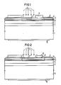
- FIG. 1 shows a possible layer structure of a conventional InGaAsP photodiode.
- an InP buffer layer 2 On the InP substrate 1, an InP buffer layer 2, an InGaAs active layer 3 and an InP cover layer 5 are grown in a lattice match.
- InGaAsP redetach protective layers 4 are additionally grown.
- the p+-doped region 7 is defined, the surface is covered with a passivation 8 and an antireflection layer 9 and the component is provided with the n-contact 10 and the p-contact 11.
- the p-contact 11 is either alloyed, as described at the beginning, or it has no purely ohmic behavior.
- the photodiode has a layer sequence or (In, GA) (As, P) / InP heterolayer structure which is analogous to the diode shown in FIG. 1, with the difference according to the invention that the p auf-doped region the p-type cover layer 5 of the InP substrate 1 as an intermediate layer, a p-type InGaAs layer 6 is epitaxially applied and structured so that it only remains under the p-contact, and thus the contact transition from the p+-doped region to p-contact 11 forms.
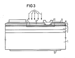
- the photodiode in turn has the InGaAsP / InP heterolayer structure shown in FIG.
- the difference according to the invention in this embodiment is that the p-type InP cover layer 5 has been removed under the p-contact 11 before it is applied.
- the p-contact 11 fills this space after it has been applied and extends through the InP cover layer to the adjacent conventional InGaAsP Reverse protection layer 4, which now takes over the function of the intermediate layer and produces the contact transition from the p-contact 11 to the p+-doped region of the p-type InP layer 5, so that this p-contact shows a purely ohmic behavior when the photodiode is operating.
Landscapes
- Light Receiving Elements (AREA)
Abstract
Description
- Die Erfindung betrifft einen ohmschen Kontakt für eine p-leitende Schicht eines InP-Substrates von Fotodioden nach dem Oberbegriff des Anspruchs 1 und ein Verfahren zu dessen Herstellung.
- Halbleiterbauelemente benötigen zu Betrieb elektrische Kontakte, durch die Versorgungs- und Signalspannungen zu- oder abgeführt werden müssen. In den meisten Fällen ist es wichtig, daß diese Kontakte ein ohmsches Verhalten zeigen, damit die Funktion des Bauelementes nicht beeinflußt wird.
- Das elektrische Verhalten von Metall-Halbleiter-Kontakten hängt von den Materialien und vom Herstellungsprozeß ab. Im Halbleitersystem InP/InGaAsP oder InP/InGaAs, das für optoelektronische Bauelemente, wie z.B. Fotodioden, im Wellenlängenbereich von 1µm bis 1,6µm angewendet wird, ist besonders das Herstellen von ohmschen Kontakten auf p-leitendem Indiumphosphid (InP) sehr schwierig.
- Bei herkömmlichen Fotodioden werden entweder legierbare p-Kontakte auf InP verwendet, oder es werden p-Kontakte akzeptiert, die kein rein ohmsches Verhalten zeigen. Im ersten Fall besteht die Gefahr, daß Metallionen aus dem p-Kontakt bis zur aktiven Schicht vordringen und unerwünschte Effekte, wie z.B. eine vorzeitige Degradation auslösen; im letzteren Fall sind Beschränkungen in der Anwendbarkeit die Folge.
- Der Erfindung liegt die Aufgabe zugrunde, einen p-Kontakt für eine p-leitende Schicht eines InP-Substrates von Fotodioden zu schaffen, der sich durch sein ohmsches Verhalten auszeichnet, wobei die p-leitende inP-Schicht, die außerhalb des Kontaktbereiches an der Oberfläche liegt, die gute Passivierbarkeit des Bauelementes und die Transparenz für die zu detektierende Strahlung gewährleisten soll, die erst in der aktiven Schicht absorbiert werden soll.
- Diese Aufgabe wird erfindungsgemäß durch einen ohmschen Kontakt mit den Merkmalen des Anspruchs 1 und ein Verfahren mit den Merkmalen der Ansprüche 2 und 3 gelöst.
- Bei der Realisierung der Erfindung wird die an sich bekannte Tatsache ausgenutzt, daß sich p-Kontakte auf p-leitendem InGaAsP und InGaAs wesentlich leichter herstellen lassen als auf InP. Dies ist sogar möglich mit Kontaktmetallisierungen, die nicht einlegiert werden müssen und bei denen folglich auch nicht das Risiko der Eindiffusion besteht.
- Ein erfindungsgemäßer ohmscher Kontakt wird entweder dadurch realisiert, daß man eine zusätzliche InGaAs- oder InGaAsP-Schicht epitaktisch aufbringt und diese so strukturiert, daß sie nur unter dem Kontakt stehen bleibt, außerhalb des Kontaktes wird diese Schicht entfernt, um eine Absorption der zu detektierenden Strahlung an der Oberfläche zu vermeiden, oder die InP-Deckschicht wird unter dem Kontakt entfernt. In beiden Fällen wird der p-Kontakt dann zum p-leitenden InGaAs oder InGaAsP hergestellt, wodurch ein ohmsches Verhalten leicht erreicht wird. Trotzdem gewährleistet die InP-Schicht, die außerhalb des Kontaktbereiches an der Oberfläche liegt, die gute Passivierbarkeit des Bauelementes und die Transparenz für die zu detektierende Strahlung, die erst in der aktiven Schicht absorbiert werden soll.
- Anhand der Figuren der Zeichnung wird die Erfindung im folgenden näher erläutert. Es zeigen:
- FIG 1 den Schichtaufbau einer herkömmlichen InGaAsP-Fotodiode
- FIG 2 und 3 Ausführungsbeispiele von InGaAsP-Fotodioden mit ohmschem p-Kontakt.
- In FIG 1 ist ein möglicher Schichtaufbau einer herkömmlichen InGaAsP-Fotodiode dargestellt. Auf dem InP-Substrat 1 werden nacheinander eine InP-Pufferschicht 2, eine InGaAs aktive schicht 3 und eine InP-Deckschicht 5 gitterangepaßt aufgewachsen. Im Falle der Flüssigphasenepitaxie werden noch zusätzlich eine oder mehrere, in diesem Beispiel zwei, InGaAsP-Rücklöseschutzschichten 4 aufgewachsen. Im Herstellungsprozeß wird das p⁺-dotierte Gebiet 7 definiert, die Oberfläche mit einer Passivierung 8 und einer Antireflexschicht 9 abgedeckt und das Bauelement mit dem n-Kontakt 10 und dem p-Kontakt 11 versehen. Der p-Kontakt 11 ist dabei, wie eingangs beschrieben, entweder einlegiert, oder er besitzt kein rein ohmsches Verhalten.
- Bei dem in FIG 2 dargestellten Ausführungsbeispiel weist die Fotodiode eine zu der in FIG 1 dargestellten Diode analoge Schichtenfolge bzw. (In, GA)(As, P)/InP-Heteroschichtstruktur auf mit dem erfindungsgemäßen Unterschied, daß auf das p⁺-dotierte Gebiet der p-leitenden Deckschicht 5 des InP-Substrates 1 als Zwischenschicht eine p-leitende InGaAs-Schicht 6 epitaktisch aufgebracht und so strukturiert ist, daß diese nur unter dem p-Kontakt stehen bleibt, und so den Kontaktübergang vom p⁺-dotierten Gebiet zum p-Kontakt 11 bildet.
- Bei dem in FIG 3 dargestellten Ausführungsbeispiel weist die Fotodiode wiederum die in FIG 1 gezeigte InGaAsP/InP-Heteroschichtenstruktur auf. Der erfindungsgemäße Unterschied besteht bei dieser Ausführungsform darin, daß die p-leitende InP-Deckschicht 5 unter dem p-Kontakt 11 vor dessen Aufbringen entfernt worden ist. Der p-Kontakt 11 füllt nach seinem Aufbringen diesen Freiraum aus und reicht durch die InP-Deckschicht hindurch bis zur angrenzenden herkömmlichen InGaAsP Rücklöseschutzschicht 4, die nunmehr die Funktion der Zwischenschicht übernimmt und den Kontaktübergang vom p-Kontakt 11 zum p⁺-dotierten Gebiet der p-leitenden InP-Schicht 5 herstellt, so daß dieser p-Kontakt beim Betrieb der Fotodiode ein rein ohmsches Verhalten zeigt.
- Die InP-Schicht 5, 7, die außerhalb des Bereiches des p-Kontaktes 11 an der Oberfläche liegt, gewährleistet die gute Passivierungsschicht 8 und die Transparenz für die zu detektierende Strahlung 12, die erst in der aktiven Schicht, d.h. der InGaAs-Schicht 3, absorbiert werden soll.
Claims (3)
dadurch gekennzeichnet, daß zwischen dem p-Kontakt (11) und einem p⁺-dotierten Gebiet (7) der p-leitenden Deckschicht (5) eine p-leitende InGaAs- oder InGaAsP-Zwischenschicht vorgesehen ist, die Teil der Schichtstruktur (4) oder eine zusätzlich eingebrachte Schicht (6) ist.
Priority Applications (1)
| Application Number | Priority Date | Filing Date | Title |
|---|---|---|---|
| EP89111873A EP0404987A1 (de) | 1989-06-29 | 1989-06-29 | Ohmscher Kontakt für eine p-leitende Schicht eines InP-Substrates von Fotodioden und Verfahren zu dessen Herstellung |
Applications Claiming Priority (1)
| Application Number | Priority Date | Filing Date | Title |
|---|---|---|---|
| EP89111873A EP0404987A1 (de) | 1989-06-29 | 1989-06-29 | Ohmscher Kontakt für eine p-leitende Schicht eines InP-Substrates von Fotodioden und Verfahren zu dessen Herstellung |
Publications (1)
| Publication Number | Publication Date |
|---|---|
| EP0404987A1 true EP0404987A1 (de) | 1991-01-02 |
Family
ID=8201556
Family Applications (1)
| Application Number | Title | Priority Date | Filing Date |
|---|---|---|---|
| EP89111873A Ceased EP0404987A1 (de) | 1989-06-29 | 1989-06-29 | Ohmscher Kontakt für eine p-leitende Schicht eines InP-Substrates von Fotodioden und Verfahren zu dessen Herstellung |
Country Status (1)
| Country | Link |
|---|---|
| EP (1) | EP0404987A1 (de) |
Cited By (1)
| Publication number | Priority date | Publication date | Assignee | Title |
|---|---|---|---|---|
| WO2017098769A1 (ja) * | 2015-12-11 | 2017-06-15 | ソニー株式会社 | 受光素子、受光素子の製造方法、撮像素子および電子機器 |
Citations (1)
| Publication number | Priority date | Publication date | Assignee | Title |
|---|---|---|---|---|
| WO1988006350A1 (en) * | 1987-02-17 | 1988-08-25 | Bt&D Technologies Limited | Capping layer fabrication |
-
1989
- 1989-06-29 EP EP89111873A patent/EP0404987A1/de not_active Ceased
Patent Citations (1)
| Publication number | Priority date | Publication date | Assignee | Title |
|---|---|---|---|---|
| WO1988006350A1 (en) * | 1987-02-17 | 1988-08-25 | Bt&D Technologies Limited | Capping layer fabrication |
Non-Patent Citations (5)
| Title |
|---|
| APPLIED PHYSICS LETTERS, Band 48, Nr. 21, 26. Mai 1986, Seiten 1416-1418, New York, US; W.T. TSANG et al.: "InGaAs/InP p-i-n- photodiodes grown by chemical beam epitaxy" * |
| ELECTRONICS LETTERS, Band 22, Nr. 17, 14. August 1986, Seiten 905-906, Stevenage, Herts, GB; J.E. BOWERS et al.: "High-speed zero-bias waveguide photodetectors" * |
| IEEE ELECTRON DEVICE LETTERS, Band EDL-6, Nr. 2, Februar 1985, Seiten 78-80, New York, US; C.C. SHEN et al.: "High conversion efficiency p-n+ InP homojunction solar cells" * |
| PATENT ABSTRACTS OF JAPAN, Band 12, Nr. 232 (E-628)[3079], 30. Juni 1988; & JP-A-63 25 985 (FUJITSU LTD) 03-02-1988 * |
| PATENT ABSTRACTS OF JAPAN, Band 9, Nr. 332 (E-370)[2055], 26. Dezember 1985; & JP-A-60 163 471 (NIPPON DENKI K.K.) 26-08-1985 * |
Cited By (4)
| Publication number | Priority date | Publication date | Assignee | Title |
|---|---|---|---|---|
| WO2017098769A1 (ja) * | 2015-12-11 | 2017-06-15 | ソニー株式会社 | 受光素子、受光素子の製造方法、撮像素子および電子機器 |
| US20180350851A1 (en) * | 2015-12-11 | 2018-12-06 | Sony Semiconductor Solutions Corporation | Light-receiving element, method of manufacturing light-receiving element, imaging device, and electronic apparatus |
| US10483299B2 (en) | 2015-12-11 | 2019-11-19 | Sony Semiconductor Solutions Corporation | Light-receiving element, method of manufacturing light-receiving element, imaging device, and electronic apparatus |
| US10943932B2 (en) | 2015-12-11 | 2021-03-09 | Sony Semiconductor Solutions Corporation | Light-receiving element, method of manufacturing light-receiving element, imaging device, and electronic apparatus |
Similar Documents
| Publication | Publication Date | Title |
|---|---|---|
| DE102008050538B4 (de) | Optoelektronisches Bauelement und Verfahren zu dessen Herstellung | |
| EP0849847B1 (de) | Optoelektronisches Bauelement mit MQW-Stukturen | |
| WO1998007187A1 (de) | Verfahren zum herstellen von halbleiterkörpern mit movpe-schichtenfolge | |
| DE2609051A1 (de) | Solarzelle | |
| DE4320780B4 (de) | Halbleiteranordnung und Verfahren zur Herstellung | |
| EP1536479B1 (de) | Strahlungsemittierendes und -empfangendes Halbleiterbauelement und Verfahren zu dessen Herstellung | |
| EP1592076B1 (de) | Optoelektronisches Bauelement mit mehreren Stromaufweitungsschichten und Verfahren zu dessen Herstellung | |
| EP1592072B1 (de) | Halbleiterchip für die Optoelektronik und Verfahren zu dessen Herstellung | |
| DE2031082A1 (de) | Anordnung fur elektronische Bauteile aus Halbleitermaterial | |
| DE3888575T2 (de) | Lichtemittierende Vorrichtung. | |
| EP1055141B1 (de) | Optische struktur und verfahren zu deren herstellung | |
| DE3135945A1 (de) | "fototransistor" | |
| DE3780239T2 (de) | Licht emittierende diode mit doppelter heterostruktur. | |
| DE10300949B4 (de) | Halbleitervorrichtung mit Herstellungsverfahren dafür | |
| DE102004026231B4 (de) | Verfahren zur Herstellung eines Bereichs mit reduzierter elektrischer Leitfähigkeit innerhalb einer Halbleiterschicht und optoelektronisches Halbleiterbauelement | |
| EP0328886B1 (de) | Isoliereinrichtung zum optischen Isolieren integrierter Komponenten | |
| EP0404987A1 (de) | Ohmscher Kontakt für eine p-leitende Schicht eines InP-Substrates von Fotodioden und Verfahren zu dessen Herstellung | |
| DE4130878C2 (de) | Verfahren zur Herstellung von aus Halbleiterschichten bestehenden Lumineszenz-Halbleiterkörpern | |
| EP0103084B1 (de) | Verfahren zur Herstellung einer planaren Avalanche-Fotodiode mit langwelliger Empfindlichkeitsgrenze über 1,3 um | |
| EP0054648A2 (de) | pn-Diode und Verfahren zu deren Herstellung | |
| WO2021244851A1 (de) | Strahlungsemittierendes bauelement und verfahren zur herstellung eines strahlungsemittierenden bauelements | |
| DE2716749A1 (de) | Optoelektronische einrichtung mit regelung der lichtausbreitung | |
| DE3605925C2 (de) | Halbleiterlaser und Verfahren zu seiner Herstellung | |
| DE10224219A1 (de) | Lichtemittierendes Halbleiterbauelement | |
| DE2827569C2 (de) |
Legal Events
| Date | Code | Title | Description |
|---|---|---|---|
| PUAI | Public reference made under article 153(3) epc to a published international application that has entered the european phase |
Free format text: ORIGINAL CODE: 0009012 |
|
| AK | Designated contracting states |
Kind code of ref document: A1 Designated state(s): AT BE CH DE ES FR GB GR IT LI LU NL SE |
|
| 17P | Request for examination filed |
Effective date: 19901220 |
|
| RBV | Designated contracting states (corrected) |
Designated state(s): DE FR GB |
|
| 17Q | First examination report despatched |
Effective date: 19921130 |
|
| APAD | Appeal reference recorded |
Free format text: ORIGINAL CODE: EPIDOS REFNE |
|
| APAD | Appeal reference recorded |
Free format text: ORIGINAL CODE: EPIDOS REFNE |
|
| APAB | Appeal dossier modified |
Free format text: ORIGINAL CODE: EPIDOS NOAPE |
|
| STAA | Information on the status of an ep patent application or granted ep patent |
Free format text: STATUS: THE APPLICATION HAS BEEN REFUSED |
|
| 18R | Application refused |
Effective date: 19991004 |
|
| APAF | Appeal reference modified |
Free format text: ORIGINAL CODE: EPIDOSCREFNE |