EP0405591B1 - Variable Blocklängenkodierung für unterschiedliche Charakteristiken der Eingangsabtastwerte - Google Patents
Variable Blocklängenkodierung für unterschiedliche Charakteristiken der Eingangsabtastwerte Download PDFInfo
- Publication number
- EP0405591B1 EP0405591B1 EP90112476A EP90112476A EP0405591B1 EP 0405591 B1 EP0405591 B1 EP 0405591B1 EP 90112476 A EP90112476 A EP 90112476A EP 90112476 A EP90112476 A EP 90112476A EP 0405591 B1 EP0405591 B1 EP 0405591B1
- Authority
- EP
- European Patent Office
- Prior art keywords
- samples
- blocks
- transform coefficients
- block
- linear transform
- Prior art date
- Legal status (The legal status is an assumption and is not a legal conclusion. Google has not performed a legal analysis and makes no representation as to the accuracy of the status listed.)
- Expired - Lifetime
Links
- 238000000034 method Methods 0.000 claims description 33
- 230000005540 biological transmission Effects 0.000 claims description 14
- 230000003044 adaptive effect Effects 0.000 claims description 9
- 230000008859 change Effects 0.000 claims description 9
- 238000004891 communication Methods 0.000 claims description 6
- 239000000523 sample Substances 0.000 description 19
- 230000008569 process Effects 0.000 description 16
- 238000010586 diagram Methods 0.000 description 13
- 230000004044 response Effects 0.000 description 10
- 230000006835 compression Effects 0.000 description 4
- 238000007906 compression Methods 0.000 description 4
- 238000013139 quantization Methods 0.000 description 4
- 101000822695 Clostridium perfringens (strain 13 / Type A) Small, acid-soluble spore protein C1 Proteins 0.000 description 2
- 101000655262 Clostridium perfringens (strain 13 / Type A) Small, acid-soluble spore protein C2 Proteins 0.000 description 2
- 101000655256 Paraclostridium bifermentans Small, acid-soluble spore protein alpha Proteins 0.000 description 2
- 101000655264 Paraclostridium bifermentans Small, acid-soluble spore protein beta Proteins 0.000 description 2
- 238000013459 approach Methods 0.000 description 2
- 238000004364 calculation method Methods 0.000 description 2
- 230000007423 decrease Effects 0.000 description 2
- 238000001514 detection method Methods 0.000 description 2
- 230000006872 improvement Effects 0.000 description 2
- 230000004048 modification Effects 0.000 description 2
- 238000012986 modification Methods 0.000 description 2
- 238000001228 spectrum Methods 0.000 description 2
- 230000006978 adaptation Effects 0.000 description 1
- 230000001419 dependent effect Effects 0.000 description 1
- 230000000694 effects Effects 0.000 description 1
- 238000011156 evaluation Methods 0.000 description 1
- 230000006870 function Effects 0.000 description 1
- 230000000737 periodic effect Effects 0.000 description 1
- 238000004513 sizing Methods 0.000 description 1
- 230000005236 sound signal Effects 0.000 description 1
- 238000012360 testing method Methods 0.000 description 1
- 230000009466 transformation Effects 0.000 description 1
Images


Classifications
-
- H—ELECTRICITY
- H03—ELECTRONIC CIRCUITRY
- H03M—CODING; DECODING; CODE CONVERSION IN GENERAL
- H03M7/00—Conversion of a code where information is represented by a given sequence or number of digits to a code where the same, similar or subset of information is represented by a different sequence or number of digits
- H03M7/30—Compression; Expansion; Suppression of unnecessary data, e.g. redundancy reduction
- H03M7/3053—Block-companding PCM systems
Definitions
- the present invention relates generally to bandwidth compression techniques for digital audio signal transmission systems, and more particularly to transform coding.
- Adaptive differential pulse-code modulation (ADPCM) technique is known as a practical way of bandwidth compression and has been extensively used in digital communications.
- ATC adaptive transform coding scheme
- ATC adaptive transform coding scheme
- input discrete speech samples are buffered to form a block of N speech samples each.
- the N samples of each block are linearly transformed into a group of transform coefficients based on a linear transform algorithm.
- transform coefficients are then adaptively quantized independently and transmitted.
- the adaptation is controlled by a short-term basis spectrum that is derived from the transform coefficients prior to quantization and transmission, and that is transmitted as a supplementary signal to the receiver.
- the short-term basis spectrum is obtained by a bit assignment process in which quantization bits are assigned corresponding to the amplitude of the transform coefficients.
- the quantized signals are adaptively dequantized in response to the supplementary signal, and an inverse transform is taken to obtain the corresponding block of reconstructed speech samples.
- block length N With an increasing value of block length N, the linear transform coding and decoding processes have increasing power of resolution with a resultant decrease in errors, and the amount of information contained in the supplementary signal decreases with the increase in block length N. This implies that for a given transmission rate a greater amount of data can be transmitted, and hence, it can lead to the quality improvement of coded signals. This is true for speech samples which can be considered as being steady for an interval corresponding to the block length N. However, with samples having a rapidly changing characteristic such as amplitude, phase and frequency, a larger value of block length does not necessarily result in small errors. Thus, it is desirable that block length N be as large as possible for signals of more stable nature, but as small as possible for signals of less stable nature. These conflicting requirements cannot be accommodated by the prior art uniform block length approach.
- US-A-4691329 relates to a video signal coding technique wherein a block of input video signal is copied and each copy of block is uniquely divided on the time and spatial domains into small blocks to produce four sets of uniquely divided small blocks. These sets of small blocks respectively undergo orthogonal transformation through encoders so that each set is compressed to a smaller number of bits.
- One of the encoded blocks is selected by evaluation according to distortion and improvement factors for delivery to the output.
- Adaptive transform coding via quad-tree based blocksize DCT is concerned with a transform coding technique using variable block size for image compression.
- the block size is adaptive to image contents necessary for trade-off between bitrate and image quality using a quadtree structure.
- Variable block sizing starts with a relatively large block size which is decomposed into subblocks by successively splitting each block into four equally-sized subblocks until the smallest blocksize is reached.
- the algorithm checks to see if the coding technique should be applied to the blocks. If the test is negative, these four adjacent N x N blocks are merged into one 2N x 2N block. The process is repeated until the blocksize reaches the maximum size.
- This object is solved with the features of claims 1 and 10.
- a sequence of input samples representing an audio-frequency signal are continuously stored into a buffer, and a change in characteristics of the input samples of successive groups is successively detected.
- the input samples of each successive group are formed into one or more blocks of optimum length which is variable in accordance with said detected characteristics change.
- the samples of each successive block are encoded into coded symbols at intervals corresponding to the length of each successive block.
- the coded symbols are multiplexed into a channel with a signal representative of the length of each successive block.
- the multiplexed signal may be recorded into a suitable recording medium or transmitted to a destination. Upon reproduction from the recording medium or upon reception through the channel, the multiplexed signal is decomposed into the coded symbols and the length-representative signal. The coded symbols are decoded at intervals corresponding to the length-representative signal.
- the input samples stored into the buffer are successively divided into a group of blocks of different lengths.
- the samples of each of the blocks are encoded into coded symbols and each block of the coded symbols is then decoded into a block of samples.
- An error between each block of decoded samples and a corresponding block of samples from the buffer is detected, and a plurality of such errors are derived from each group of blocks of input samples.
- a minimum value of the errors is then determined and one of the blocks of the coded symbols which corresponds to the minimum error is identified as having an optimum block length.
- the coded symbols of the optimum block length are multiplexed with a signal indicating the optimum block length into a channel for purposes of either transmission or recording.
- a communication system which comprises a buffer, a buffer controller for storing audio-frequency digital samples into the buffer and reading the stored samples from the buffer to produce a sequence of blocks of samples of different lengths.
- An encoder is coupled to the buffer for encoding the samples of each of the blocks into coded symbols and a first decoder is coupled to the encoder for decoding the coded symbols into decoded samples in a process inverse to the encoder.
- An error detector is coupled to the buffer and to the decoder for detecting an error between each block of the decoded samples and a corresponding block of samples from the buffer.
- a memory is provided for storing errors detected by the error detector from the sequence of blocks of samples.
- a minimum detector detects a minimum value of the errors in the memory and generates a signal identifying one of the blocks of the coded symbols which corresponds to the minimum value as having an optimum block length.
- a multiplexer multiplexes the coded symbols of the optimum block length with the optimum length signal into a channel for transmission from a transmit end of the system.
- a demultiplexer receives a multiplexed signal through the channel and decomposes the multiplexed signal into the coded symbols and the optimum length signal.
- a second decoder is coupled to the demultiplexer for decoding the coded symbols at intervals corresponding to the optimum length indicated by the demultiplexed optimum length signal.
- a communications system employing an adaptive linear transform coding and decoding scheme according to the present invention.
- an audio-frequency signal either speech or music
- an input terminal 1 If the input signal is of analog form, it is applied to an A/D converter 2 in which it is sampled at the Nyquist rate and quantized into digital samples and fed to a buffer 3. If the input signal is of digital form it is supplied directly to the buffer.
- each successive group of 4N input samples is sequentially divided into blocks of N, 2N and 4N output samples with a total of 7N samples in a manner as will be described.
- the output of buffer 3 is preferably passed through a normalizer 4 to an encoder 5 whose output is coupled to a decoder 6 for error detection and minimum error detection on the one hand, and to a data selection and multiplexing circuit 11 for transmission on the other.
- a minimum detector 9 takes its inputs from memory 8 to receive a first error value E(N) derived from the first N-sample block, a second error value E(2N) derived from the first subblock of the second 2N-sample block as a representative value of that block, and a third error value E(4N) derived from the first subblock of the third 4N-sample block as its representative value.
- Minimum error detector 9 searches the input error values and detects which one of these is of the least value and identifies the block of least error as a block of optimum length. This optimum length block is identified as a block in which a characteristic change in factors such as amplitude, phase and frequency has occurred.
- minimum error detector 9 is coupled to the data selection and multiplexing circuit 11 to transmit a signal representative of the optimum block length as supplementary information. This signal is further applied to buffer controller 10 to cause it to shift the contents of buffer 3 to discard samples corresponding in number to the samples contained in the block identified as an optimum block length.
- Encoder 5 comprises a linear transform coding circuit 21, a bit assignment circuit 22, and a quantizer 23.
- linear transform coding circuit 21 provides linear transform coding on each variable-length block of samples from the output of normalizer 4 at variable intervals corresponding to the length of each block to generate a series of 2 0 N, 2 1 N .... 2 m N transform coefficients.
- the Walsh-Hadamard transform, the discrete Fourier transform, the discrete cosine transform and the Karhunen-Loéve transform are suitable linear transform coding for this invention.
- Quantizer 23 is connected to the output of linear transform coding circuit 22.
- Quantizer 23 includes a maximum of 2 m N quantizer elements for successively quantizing the 2 0 N, 2 1 N, .... 2 m N transform coefficients using an optimum number of bits supplied from bit assignment circuit 21 whose function is to minimize squared errors resulting from quantization and dequantization processes.
- the output of quantizer 31 is dequantized by a dequantizer 32 and fed to an interpolator 33 in which the logarithm to the base 2 is taken of the dequantized samples and (M-1) interpolations are provided between successive input samples.
- the output of interpolator 33 is fed to a step size optimizer 34 in which the following Equation is calculated: where, R i is the number of bits assigned to ith transform coefficient, R ⁇ is the average number of bits assigned to each transform coefficient, and ⁇ i 2 is a squared value of the ith interpolated transform coefficient.
- the output of quantizer 23 is supplied to multiplexing circuit 11 and transmitted as main information on the one hand, and supplied on the other to a dequantizer 24 which forms part of decoder 6.
- Dequantizer 24 is also supplied with the interpolated output of bit assignment circuit 21 to perform a process inverse to that of quantizer 23.
- the output of dequantizer 24 is fed to an inverse linear transform coder 25 to generate a replica of the samples corresponding to those appearing at the output of normalizer 4. It is seen that all processes performed by encoder 5 and decoder 6 on each block of samples must be completed before the next block of samples is supplied from buffer 3.
- normalizer 4 causes linear transform coder 21 to produce an output whose value is not dependent on the power level of the input signal.
- normalizer 4 comprises a buffer 40, a variance calculator 41 and a scaling circuit 42.
- Each variable-length block of samples is stored into buffer 40 and the variance of the samples is derived to produce a signal representative of an average power of each block.
- the output of variance calculator 41 is supplied to the multiplexer 11 and transmitted as supplementary information on the one hand, and used on the other by scaler 42 to modify the values of the stored samples before being applied to linear transform coder 21.
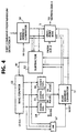
- buffer controller 10 Description of details of buffer controller 10 according to the first embodiment of the invention will now be given below with reference to Figs. 4 to 7.
- buffer controller 10 includes a write address generator 50 which generates a write address by counting a high-frequency clock and sequentially writes input samples from A/D converter 2 into buffer 3 which is shown as a dual-port random access memory.
- the stored samples are retrieved from RAM 3 by a read address generator 51 simultaneously with the write operation.
- the amount of samples remaining in RAM 3 is represented by the difference between the write and read address values, this difference being detected by a subtractor 52.
- a ring counter 53 is enabled by subtractor 52 to start counting low-frequency clock and sequentially applies an output pulse to high-frequency clock generators 54, 55 and 56 as well as to an OR gate 57.
- Clock generators 54, 55 and 56 generate different numbers of high-frequency pulses in burst form so that N clock pulses are supplied from clock generator 54 to the count input of read address generator 51 in response to a first ring counter output, 2N clock pulses are supplied from clock generator 55 in response to a second ring counter output and 4N clock pulses are supplied from clock generator 56 in response to a third ring counter output.
- the output of OR gate 57 is supplied to the reset input of read address generator 51 so that when it is reset its address increments from a zero count corresponding to the first storage location of RAM 3.
- Write address generator 50 responds to the output of minimum error detector 9 as a shift command signal by shifting the storage locations of RAM 3 by an amount equal to the optimum block length so that the same number of samples as those contained in the optimum block length are discarded from RAM 3 and newer samples fill in their places each time an optimum block length decision is made.
- buffer controller of Fig. 4 will be understood with reference to Fig. 5. It is assumed that the minimum error detector 9 sequentially determines that block lengths N, 4N and 2N are sequentially optimum for a sequence of three groups of N, 2N and 4N output samples each (with a total of 21N output samples) when a sequence of 9N input samples are stored into RAM 3.
- subtractor 52 When 4N samples are initially stored into RAM 3 at time t 1 , subtractor 52 generates an output which causes ring counter 53 to enable clock generator 54 to supply N clock pulses to the read address generator 51, thus reading N samples from the first to the Nth sample storage locations of RAM 3 as indicated by an arrow A and fed to normalizer 4 as a first block of group G1.
- clock generator 55 is enabled by ring counter 53 to supply 2N pulses to address generator 51 to cause it to read 2N samples (first and second blocks) from the first to the 2Nth sample storage locations of RAM 3 as indicated by an arrow B and fed to normalizer 4 as a second block of group G1.
- Clock generator 56 is then enabled to supply 4N pulses to address generator 51 to read 4N samples (first to fourth blocks) from the first to the 4Nth sample storage locations of RAM 3 as indicated by an arrow C and fed to the normalizer as a third block of group G1.
- Coding/decoding and error computations are successively performed on each of these N, 2N and 4N samples of group G1. If these processes are completed within a period T1 from the time of delivery of the third block of group G1, a decision will be made by minimum error detector 9 at time t 2 on the group G1 samples in favor of N block length. N samples will be discarded and the remaining 3N samples (second to fourth blocks) are shifted from the first to 3Nth storage locations and new N samples (fifth block) are added, causing subtractor 52 to supply the next output pulse to ring counter 53.
- a third decision is made by minimum error detector 9 in favor of 2N block length at time t 5 , causing RAM 3 to discard 2N samples, leaving eighth and ninth samples to which tenth N samples are newly added.
- a group G4 of output samples is then read out of RAM 3 when new eleventh N samples are subsequently written into RAM 3.
- buffer controller 10 includes a write address generator 60 which generates a write address to sequentially write input samples into buffer 3 as in Fig. 4.
- the amount of samples remaining in RAM 3 is detected by a subtractor 62 by comparison between the write address supplied from read address generator 60 and a read address generated by a read address generator 61.
- Subtractor 62 generates first, second and third output signals respectively when the stored samples successively reach a count N, 2N and 4N.
- a controller 63 is provided to receive the outputs of subtractor 62 as well as a shift command signal from detector 9 to enable clock generators 64, 65 and 66 in succession. The outputs of controller 63 are fed to an OR gate 67 to reset the read address generator 61 in the same manner as in Fig. 4.
- buffer controller of Fig. 6 will be understood with reference to Fig. 7.
- the minimum error detector 9 sequentially determines that block lengths N, 4N and 2N are sequentially optimum for a sequence three groups of N, 2N and 4N samples in response to a sequence of 9N input samples.
- controller 63 enables clock generator 64 to supply N clock pulses to the read address generator 61 to cause it to read N samples from the first to the Nth storage locations of RAM 3 for application to normalizer 4.
- the stored samples reach count 2N and controller 63 enables clock generator 65 to supply 2N clock pulses to address generator 61 to read 2N samples out of the first to the 2Nth storage locations of RAM 3.
- the stored samples reach count 4N and controller 63 enables clock generator 66 to supply 4N clock pulses to address generator 61 to read 4N samples out of the first to the 4Nth storage locations of RAM 3.
- N , 2N and 4N samples are successively delivered from RAM 3 as a corresponding number of input samples is successively stored in RAM 3.
- coding/decoding processes and error calculation are performed and errors derived from these samples are stored in memory 8 before the third block of output samples are read out of RAM 3.
- subtractor 62 Since 3N samples remain in RAM 3 at time t 4 , subtractor 62 will generate an output (2N), causing controller 63 to successively enable clock generators 64 and 65 so that N samples are read out of the first to Nth storage locations of RAM 3 as indicated by arrow a and delivered as a first block of group G2, and then 2N samples are read out of the first to 2Nth storage locations of RAM 3 as indicated by arrow b and delivered as a second block of group G2. At time t 5 , new N samples (fifth block) will be stored in RAM 3 giving a total of 4N samples. Subtractor 62 supplies an output (4N) to controller 63 to read 4N samples (second to fifth blocks) as a third block of group G2.
- Subtractor 62 generates an output (4N) to read the sixth to ninth N samples of group G3.
- a minimum error decision will be taken in favor of 2N block length to discard the sixth and seventh samples, leaving the eighth and ninth samples.
- Subtractor 62 generates an output (2N) to read the eighth N samples as N samples of group G4 as indicated by arrow c and then the eighth and ninth N samples are read as 2N samples of G4 as indicated by arrow d .
- new tenth and eleventh N samples are stored, giving a total of 4N samples and these samples are read as 4N samples of G4.
- data selection and multiplexing circuit 11 includes a multiplexer 70 in which the main information signal supplied from quantizer 23 and supplementary information signals from bit assignment circuit 22 and normalizer 4 are multiplexed into a single variable-length block of data corresponding to each variable-length block of samples retrieved from buffer 3.
- the multiplexed blocks are successively stored into respective locations of a memory 71 and supplied to a selector 72 to which the output of minimum error detector 9 is also applied.
- selector 72 reads the corresponding block out of memory 71 into a multiplexer 73 in which it is multiplexed with the optimum block length signal into a sequence of samples and transmitted over a transmission line 12 to the receiver.
- bit assignment circuit 15 is made up of a dequantizer 80, an interpolator 81 and a step-size optimizer 82.
- the demultiplexed step-size value signal is dequantized by dequantizer 80 and fed to interpolator 81 which provides interpolations in much the same way as interpolator 33 of the transmitter.
- Step-size optimizer 82 also corresponds to the step-size optimizer 34 of the transmitter to determine the optimum quantization step-size by computing Equation (1).
- dequantizer 14 uses the step-size determined by the optimizer 82, dequantizer 14 recovers a replica of the original transform coefficients and supplies it to an inverse linear transform coder 17 whose output is connected to denormalizer 18.
- the demultiplexed optimum block length signal is applied to a block timing circuit 16 in which it is converted to a block timing signal indicating the end of a received block of transform coefficients.
- inverse linear transform coder 17 performs inverse linear transform on the dequantized transform coefficients to recover a replica of the original digital speech/music samples and applies it to denormalizer 18.
- denormalizer 18 includes a scaler 90 which multiplies the output of inverse linear transform coder 17 by a reciprocal of the demultiplexed variance signal.
- the output of scaler 90 is fed to a buffer 91 whose output is converted to analog form by a D/A converter 19 to produce a replica of the original analog speech/music signal at an output terminal 20.
- buffer 3 is controlled by a buffer controller 100 which operates independently of the output of a minimum detector 104 to read a sequence of seven variable length blocks of samples.
- a memory 101 is coupled to the error detector 7 to store a group of seven errors which are respectively derived from the blocks.
- First four outputs of memory 100 are connected to a first average circuit 102 and the fifth and sixth outputs of the memory are connected to a second average circuit 103.
- the outputs of average circuits 102 and 103 are coupled to minimum detector 104 to which the seventh output of memory 101 is also applied.
- Fig. 12 details of buffer controller 100 are illustrated. Each successive group of 4N input samples stored in buffer 3 is sequentially divided into seven blocks of N, N, 2N, N, N, 2N and 4N output samples, a total of 12N output samples.
- Write and read address generators 110 and 111 are provided as in the first embodiment of this invention.
- Subtractor 112 detects the amount of samples stored in RAM 3 by making a comparison between the write and read addresses as in the previous embodiments. In this embodiment, subtractor 112 generates four output signals (N), (2N), (3N) and (4N) when the stored sample count reaches N, 2N, 3N and 4N, respectively.
- the outputs of subtractor 112 are fed to a controller 113 having output terminals designated N, 2N, 2N+ ⁇ , 3N, 4N, 4n+ ⁇ , and 4N+2 ⁇ .
- the output terminals N, 2N 3N and 4N of controller 113 are coupled together to a clock generator 116 which generates N clock pulses in burst form, and the output terminals 2N+ ⁇ and 4N+ ⁇ are coupled through an OR gate 115 to a clock generator 107 which generates 2N clock pulses.
- the output terminal 4N+2 ⁇ of controller 113 is connected to a clock generator 118 which generates 4N clock pulses.
- the outputs of clock generators 116, 117 and 118 are coupled to the count input of the read address generator 101.
- the read address generator 111 is reset to zero count in response to a signal from the output terminal 2N+ ⁇ and 4N+2 ⁇ which are connected through an OR gate 114. Address generator 111 is further reset to a 2N count in response to a signal from the 4N+ ⁇ output terminal of controller 113. At periodic intervals, controller 113 supplies a clear pulse to write address generator 110 to discard all samples in RAM 3 to refill it with new input samples. This clear pulse is also applied to the read address generator 111 via OR gate 114.
- buffer controller 100 will be understood with reference to Fig. 13.
- clear pulse is supplied to both address generators.
- subtractor 112 supplies an output (N) to controller 113, which generates an output at the output terminal N.
- Clock generator 116 is enabled to supply N clock pulses to the read address generator 111 to read the first block of N samples from RAM 3 as a first block of output samples.
- a second block of N input samples is stored into RAM 3 and subtractor 112 generates an output signal (2N).
- Controller 113 applies a signal to its output terminal 2N so that the read address generator 111 is incremented further by a 2N count to read the second block of N samples as a second block of output samples. Subsequently, controller 113 applies a signal to the 2N+ ⁇ output terminal.
- Clock generator 117 is enabled to supply 2N clock pulses to the read address generator 111 to read first and second N samples as a third block of output samples.
- controller 113 applies a signal to the 3N output terminal to enable clock pulse generator 106.
- the read address generator 111 is thus incremented by N from the previous 2N count value and the third N samples are read out of RAM 3 as a fourth block of output samples.
- Controller 113 applies a signal to the 4N output terminal to enable clock pulse generator 116.
- the read address generator 111 is thus incremented further by N from the previous 3N count value and the fourth N samples are read out of RAM 3 as a fifth block of output samples.
- controller 113 sequentially applies a signal to its 4N+ ⁇ output terminal to cause clock generator 117 to supply 2N clock pulses to the read address generator 111 as well as to its reset-to-2N input terminal.
- the address generator 111 is incremented by a 2N count from the previous 2N address count to read the third and fourth N samples from RAM 3 as a sixth block of output samples. Controller 113 then applies a signal to its 4N+2 ⁇ output terminal. This signal resets the address generator 111 to zero and causes clock generator 118 to increment the address generator 111 by a 4N count from zero. As a result, the first to fourth N samples are read out of RAM 3 as a seventh block of output samples. Controller 113 then clears the write and read address generators to repeat the above process to successively read a group of seven blocks of output samples. It is seen from Fig.
- each sequence of seven variable length blocks contains an equal number of groups of N sample subblocks of different arrivals, i.e., three subblocks of first arrivals, three subblocks of second arrivals, three subblocks of third arrivals and finally three subblocks of fourth arrivals.
- the linear transform coder 21 and inverse linear transform coder 25 provide coding/decoding processes at variable intervals corresponding to each block of different length.
- each block undergoes an error computation process in which an error between each block at the output of inverse liner transform coder 25 and a corresponding block at the output of normalizer 4 is detected and stored into memory 8.
- the sample sequence is treated on a block-by-block basis by the encoder 5 and decoder 6 as if it were organized into a first group of four blocks of N samples each, a second group of two blocks of 2N samples each, and a block of 4N samples as a third group as shown in Fig. 14A.
- N 1 , N 2 , N 3 and N 4 are treated as a first group containing four blocks N 1 , N 2 , N 3 and N 4 of one-subblock length, a second group of two blocks “N 1 and N 2 " and “N 3 and N 4 " of two-subblock length and a third group of "N 1 ,N 2 , N 3 and N 4 " of four-subblock length.
- E(N 1 ), E(N 2 ), E(N 3 ) and E(N 4 ) are derived respectively from the blocks of the first group and two errors E(N 1 + N 2 ) and E(N 3 + N 4 ) are derived respectively from the two blocks of the second group, and a single error E(N 1 +N 2 +N 3 +N 4 ) is derived from the block of the third group.
- These seven error values are stored in respective locations of memory 101.
- Average circuit 102 takes an average value of the errors E(N 1 ), E(N 2 ), E(N 3 ) and E(N 4 ) and average circuit 103 takes an average value of the errors E(N 1 + N 2 ) and E(N 3 + N 4 ).
- Minimum error detector 104 compares these averaged errors and the error E(N 1 +N 2 +N 3 +N 4 ) against each other and detects a minimum value, and classifies those blocks of the minimum error as having an optimum block length.
- Data selector 72 selects the transform coefficients of the blocks having the optimum block length from memory 71 for transmission.
- optimum block length is N, transform coefficients corresponding to one-subblock length samples N 1 , N 2 , N 3 and N 4 are selected, and if the optimum block length is 2N, transform coefficients corresponding to two-subblock length samples "N 1 and N 2 " and "N 3 and N 4 " are selected.
- optimum block length 4N those corresponding to the four-subblock length samples "N 1 +N 2 +N 3 +N 4 " are selected for transmission.
- the sample sequence is organized into a first group of sixteen blocks of N samples each, a second group of eight blocks of 2N samples each, a third group of four blocks of 4N samples each, a fourth group of two blocks of 8N samples each, and a fifth group of 16N samples, as illustrated in Fig. 14C.
Landscapes
- Engineering & Computer Science (AREA)
- Theoretical Computer Science (AREA)
- Compression, Expansion, Code Conversion, And Decoders (AREA)
- Transmission Systems Not Characterized By The Medium Used For Transmission (AREA)
Claims (17)
- Adaptives Transformationskodierungsverfahren, mit den Schritten:(a) Speichern einer Abfolge von Eingangsabtastwerten von zugrundeliegenden Tonfrequenzsignalen in einen Zwischenspeicher (3),(b) aufeinanderfolgendes Aufteilen einer Gruppe von gespeicherten Abtastwerten in mehrere Blöcke,(c) Kodieren jedes der Blöcke in kodierte Zeichen,(d) Ableiten eines zusätzlichen Signals von den kodierten Zeichen, und(e) Multiplexen des zusätzlichen Signals mit den kodierten Zeichen zur Übertragung oder Speicherung,gekennzeichnet durch die Schritte:(f) Ermitteln einer Änderung der Charakterstiken, wie Phase, Amplitude und Frequenz, der Eingangsabtastwerte von aufeinanderfolgenden Gruppen und Bestimmen einer optimalen Blocklänge entsprechend der ermittelten Änderung der Charakteristiken,(g) Lesen der Eingangsabtastwerte jeder Gruppe aus dem Zwischenspeicher und Anordnen der Abtastwerte in eine Abfolge von Blöcken unterschiedlicher Längen, wobei die Blöcke größerer Länge Eingangsabtastwerte späteren Eintreffens enthalten und Kopien von Eingangsabtastwerten früheren Eintreffens, die in den Blöcken kleinerer Länge enthalten sind,(h) Auswählen eines der Blöcke entsprechend der optimalen Blocklänge, und(i) Erzeugen eines die optimale Blocklänge anzeigenden Signals als das zusätzliche Signal.
- Verfahren nach Anspruch 1, wobei der Schritt (f) die Schritte aufweist:(f1) Dekodieren der kodierten Zeichen,(f2) Ermitteln von Abweichungen zwischen den dekodierten Zeichen und den Zeichen, die in den Blöcken der Abfolge enthalten sind, und(f3) Ermitteln eines Minimalwertes der Abweichung als die ermittelte Änderung der Charakteristiken.
- Verfahren nach Anspruch 1 oder 2, wobei jeder der Blöcke unterschiedlicher Längen einen oder mehrere Teilblöcke von jeweils N Abtastwerten aufweist, und wobei jeder der Blöcke unterschiedlicher Blocklängen 2kN Abtastwerte enthält, wobei k eine ganzzahlige Variable in einem Bereich von 0 bis zu einem vorherbestimmten Maximalwert ist.
- Verfahren nach Anspruch 1 oder 2, wobei die Blöcke unterschiedlicher Längen (m+1) Gruppen von 2i Blöcken von 2jN Abtastwerten aufweisen, die jeweils aus 21+jN aus dem Zwischenspeicher ausgelesenen Abtastwerten aufgebaut sind, wobei i + j = m, und i eine Variable in einem Bereich von m bis 0 ist und j eine Variable in einem Bereich von 0 bis m ist, und wobei m gleich oder größer als 2 ist, und N ein ganze Zahl ist, wobei jede der Gruppen eine gleiche Summe von Abtastwerten gleichen Eintreffens enthält.
- Verfahren nach einem der vorhergehenden Ansprüche, das die Schritte aufweist: Ableiten einer Abweichung der Abtastwerte jedes aufeinanderfolgenden Blockes und Skalieren der Abtastwerte mit der Abweichung, und Multiplexen der Abweichung mit den kodierten Zeichen in den Kanal.
- Verfahren nach einem der vorhergehenden Ansprüche, wobei die kodierten Zeichen lineare Transformationskoeffizienten sind.
- Verfahren nach Anspruch 6, das die Schritte aufweist: Bestimmen einer Schrittweite aus den linearen Transformationskoeffizienten und Quantisieren der linearen Transformationskoeffizienten entsprechend der Schrittweite vor dem Schritt (h), und Multiplexen der Schrittweite mit den quantisierten linearen Transformationskoeffizienten in den Kanal.
- Verfahren nach Anspruch 7, wobei die Schrittweite durch die Schritte bestimmt wird: Quadrieren der linearen Transformationskoeffizienten und Nehmen eines Mittelwerts einer Gruppe der quadrierten linearen Transformationskoeffizienten, die benachbart vorkommen, als einen repräsentativen Wert der Gruppe, Multiplexen der linearen Transformationskoeffizienten mit dem Mittelwert, Bereitstellen von Interpolationen zwischen aufeinanderfolgenden der quadrierten linearen Transformationskoeffizienten, und Ableiten der Schrittweite aus den interpolierten quadrierten linearen Transformationskoeffizienten.
- Verfahren nach einem der vorhergehenden Ansprüche, das die Schritte aufweist: Demultiplexen der kodierten Zeichen und des die Länge anzeigenden Signals, und Dekodierung der demultiplexten kodierten Zeichen entsprechend dem demultiplexten, die Länge anzeigenden Signal.
- Übertragungssystem, das aufweist: einen Zwischenspeicher (3), Zwischenspeicher-Steuereinrichtungen (10;100) zum Speichern einer Abfolge von Eingangsabtastwerten zugrundeliegender Tonfrequenzsignale, wie Sprache und Musik, in den Zwischenspeicher und Anordnen der gespeicherten Eingangsabtastwerte einer aufeinanderfolgenden Gruppe in mehreren Blöcken, und Kodiereinrichtungen (5) zum Kodieren der Abtastwerte jedes aufeinanderfolgenden Blockes in kodierte Zeichen, basierend auf einem adaptiven Übertragungskodierungsverfahren, und Ableiten eines zusätzlichen Signals aus den kodierten Zeichen, Multiplexereinrichtungen (11) zum Multiplexen der zusätzlichen Signale mit den kodierten Zeichen, um Multiplexsignale zur Übertragung durch einen Kanal (12) oder Speichern in einem Speichermedium zu erzeugen, Demultiplexereinrichtungen (13) zum Aufspalten des durch den Kanal empfangenen oder aus dem Speichermedium zurückgewonnenen Multiplexsignals, und Dekodiereinrichtungen (14-18) zum Dekodieren der demultiplexten kodierten Zeichen entsprechend dem demultiplexten zusätzlichen Signal,
dadurch gekennzeichnet, daßdie Zwischenspeicher-Steuereinrichtungen (10;100) die gespeicherten Eingangsabtastwerte der Gruppe in eine Abfolge von Blöcken unterschiedlicher Längen anordnen, wobei die Blöcke größerer Länge Eingangsabtastwerte späteren Eintreffens und Kopien von Eingangsabtastwerten früheren Eintreffens enthalten, die in den Blöcken kleinerer Länge enthalten sind,Einrichtungen (6,7,8,9) zur Bestimmung der optimalen Länge bereitgestellt werden zum Ermitteln einer Änderung der Charakteristiken, wie Phase, Amplitude und Frequenz, der gespeicherten Eingangsabtastwerte von aufeinanderfolgenden Gruppen und Bestimmen einer optimalen Blocklänge entsprechend der Charakteristikänderung und Auswählen eines der Blöcke entsprechend der optimalen Blocklänge, und Erzeugen eines die optimale Blocklänge anzeigenden Signals, unddie Multiplexereinrichtungen (11) das längenanzeigende Signal als das zusätzliche Signal zum Multiplexen mit den kodierten Zeichen verwenden, um das Multiplexsignal zu erzeugen. - System nach Anspruch 10, wobei die Einrichtungen (6,7,8,9) zur Bestimmung der optimalen Länge aufweisen: Dekodiereinrichtungen (6) zum Dekodieren der kodierten Zeichen, Abweichungsdetektoreinrichtungen (7) zum Ermitteln von Abweichungen zwischen den dekodierten Zeichen und den in den Blöcken der Abfolge enthaltenen Zeichen, und Minimalabweichungsdetektoreinrichtungen (8,9) zum Ermitteln eines Minimalwerts der Abweichungen als die ermittelte Änderung der Charakteristiken.
- System nach Anspruch 10 oder 11, dadurch gekennzeichnet, daß jeder der Blöcke unterschiedlicher Längen einen oder mehrere Teilblöcke von jeweils N Abtastwerten aufweist, und daß jeder der Blöcke unterschiedlicher Blocklängen 2kN Abtastwerte enthält, wobei k eine ganzzahlige Variable in einem Bereich von 0 bis zu einem vorherbestimmten Maximalwert ist.
- System nach Anspruch 10 oder 11, dadurch gekennzeichnet, daß die Blöcke unterschiedlicher Längen (m+1) Gruppen von 2i Blöcken von jeweils 2jN Abtastwerten aufweist, die aus 2i+jN aus dem Zwischenspeicher ausgelesenen Abtastwerten aufgebaut sind, wobei i + j = m, und i eine Variable in einem Bereich von m bis 0 ist und j eine Variable in einem Bereich von 0 bis m ist, und wobei m gleich oder größer als 2 ist, und N eine ganze Zahl ist, wobei jeder der Gruppen eine gleiche Anzahl von Abtastwerten gleichen Eintreffens enthält.
- System nach einem der vorhergehenden Ansprüche, das aufweist: Einrichtungen (41) zum Ableiten einer Abweichung der Abtastwerte jedes aufeinanderfolgenden Blockes und Einrichtungen (42) zum Skalieren der Abtastwerte mit der Abweichung und Anlegen der skalierten Abtastwerte an die Einrichtungen zur Bestimmung der optimalen Länge und zum Veranlassen der Multiplexereinrichtungen, die Abweichung mit den kodierten Zeichen zur Übertragung an dem Kanal zu multiplexen.
- System nach einem der vorhergehenden Ansprüche, wobei die kodierten Zeichen lineare Transformationskoeffizienten sind.
- System nach Anspruch 15, das aufweist: Einrichtungen (22) zum Bestimmen einer Schrittweite aus den linearen Transformationskoeffizienten und Einrichtungen (23) zum Quantisieren der linearen Transformationskoeffizienten entsprechend der Schrittweite und zum Veranlassen der Multiplexereinrichtungen, die Schrittweite mit den quantisierten linearen Transformationskoeffizienten zur Übertragung an den Kanal zu multiplexen.
- System nach Anspruch 16, wobei die Einrichtungen (22) zum Bestimmen der Schrittweite aufweisen: Einrichtungen (30) zum Quadrieren der linearen Transformationskoeffizienten, Nehmen eines Mittelwerts einer Gruppe der quadrierten linearen Transformationskoeffizienten, die benachbart vorkommen, als einen repräsentativen Wert der Gruppe und Veranlassen der Multiplexereinrichtungen, die linearen Transformationskoeffizienten mit dem Mittelwert zur Übertragung an den Kanal zu multiplexen, Einrichtungen (33) zum Bereitstellen von Interpolationen zwischen aufeinanderfolgenden der quadrierten linearen Transformationskoeffizienten und Ableiten der Schrittweite von den interpolierten quadrierten linearen Transformationskoeffizienten.
Applications Claiming Priority (6)
| Application Number | Priority Date | Filing Date | Title |
|---|---|---|---|
| JP1170068A JP2638208B2 (ja) | 1989-06-30 | 1989-06-30 | 適応変換符号化復号化の方法及び装置 |
| JP170069/89 | 1989-06-30 | ||
| JP1170069A JP2778128B2 (ja) | 1989-06-30 | 1989-06-30 | 適応変換符号化の方法及び装置 |
| JP170068/89 | 1989-06-30 | ||
| JP24551489A JP2923996B2 (ja) | 1989-09-20 | 1989-09-20 | 適応変換符号化の方法及び装置 |
| JP245514/89 | 1989-09-20 |
Publications (3)
| Publication Number | Publication Date |
|---|---|
| EP0405591A2 EP0405591A2 (de) | 1991-01-02 |
| EP0405591A3 EP0405591A3 (en) | 1991-11-06 |
| EP0405591B1 true EP0405591B1 (de) | 1997-10-01 |
Family
ID=27323291
Family Applications (1)
| Application Number | Title | Priority Date | Filing Date |
|---|---|---|---|
| EP90112476A Expired - Lifetime EP0405591B1 (de) | 1989-06-30 | 1990-06-29 | Variable Blocklängenkodierung für unterschiedliche Charakteristiken der Eingangsabtastwerte |
Country Status (3)
| Country | Link |
|---|---|
| US (1) | US5166686A (de) |
| EP (1) | EP0405591B1 (de) |
| DE (1) | DE69031517T2 (de) |
Families Citing this family (37)
| Publication number | Priority date | Publication date | Assignee | Title |
|---|---|---|---|---|
| US5502789A (en) * | 1990-03-07 | 1996-03-26 | Sony Corporation | Apparatus for encoding digital data with reduction of perceptible noise |
| CN1062963C (zh) * | 1990-04-12 | 2001-03-07 | 多尔拜实验特许公司 | 用于产生高质量声音信号的解码器和编码器 |
| JP2973675B2 (ja) * | 1991-07-22 | 1999-11-08 | 日本電気株式会社 | 可変レート伝送に適した符号化復号方式及び装置 |
| ES2164640T3 (es) * | 1991-08-02 | 2002-03-01 | Sony Corp | Codificador digital con asignacion dinamica de bits de cuantificacion. |
| JP3178026B2 (ja) * | 1991-08-23 | 2001-06-18 | ソニー株式会社 | ディジタル信号符号化装置及び復号化装置 |
| DE69227570T2 (de) * | 1991-09-30 | 1999-04-22 | Sony Corp., Tokio/Tokyo | Verfahren und Anordnung zur Audiodatenkompression |
| JP3134455B2 (ja) * | 1992-01-29 | 2001-02-13 | ソニー株式会社 | 高能率符号化装置及び方法 |
| JP3153933B2 (ja) * | 1992-06-16 | 2001-04-09 | ソニー株式会社 | データ符号化装置及び方法並びにデータ復号化装置及び方法 |
| JP3127600B2 (ja) * | 1992-09-11 | 2001-01-29 | ソニー株式会社 | ディジタル信号復号化装置及び方法 |
| JP3508146B2 (ja) * | 1992-09-11 | 2004-03-22 | ソニー株式会社 | ディジタル信号符号化復号化装置、ディジタル信号符号化装置及びディジタル信号復号化装置 |
| JP3343962B2 (ja) * | 1992-11-11 | 2002-11-11 | ソニー株式会社 | 高能率符号化方法及び装置 |
| JP3185413B2 (ja) * | 1992-11-25 | 2001-07-09 | ソニー株式会社 | 直交変換演算並びに逆直交変換演算方法及びその装置、ディジタル信号符号化及び/又は復号化装置 |
| JP3123286B2 (ja) * | 1993-02-18 | 2001-01-09 | ソニー株式会社 | ディジタル信号処理装置又は方法、及び記録媒体 |
| US5459850A (en) * | 1993-02-19 | 1995-10-17 | Conner Peripherals, Inc. | Flash solid state drive that emulates a disk drive and stores variable length and fixed lenth data blocks |
| JP3123290B2 (ja) * | 1993-03-09 | 2001-01-09 | ソニー株式会社 | 圧縮データ記録装置及び方法、圧縮データ再生方法、記録媒体 |
| US5510785A (en) * | 1993-03-19 | 1996-04-23 | Sony Corporation | Method of coding a digital signal, method of generating a coding table, coding apparatus and coding method |
| JP3173218B2 (ja) * | 1993-05-10 | 2001-06-04 | ソニー株式会社 | 圧縮データ記録方法及び装置、圧縮データ再生方法、並びに記録媒体 |
| US5717821A (en) * | 1993-05-31 | 1998-02-10 | Sony Corporation | Method, apparatus and recording medium for coding of separated tone and noise characteristic spectral components of an acoustic sibnal |
| KR100368854B1 (ko) * | 1993-06-30 | 2003-05-17 | 소니 가부시끼 가이샤 | 디지털신호의부호화장치,그의복호화장치및기록매체 |
| TW272341B (de) * | 1993-07-16 | 1996-03-11 | Sony Co Ltd | |
| TW327223B (en) * | 1993-09-28 | 1998-02-21 | Sony Co Ltd | Methods and apparatus for encoding an input signal broken into frequency components, methods and apparatus for decoding such encoded signal |
| EP0692880B1 (de) * | 1993-11-04 | 2001-09-26 | Sony Corporation | Signalkodierer, signaldekodierer, aufzeichnungsträger und signalkodiererverfahren |
| WO1995013660A1 (en) * | 1993-11-09 | 1995-05-18 | Sony Corporation | Quantization apparatus, quantization method, high efficiency encoder, high efficiency encoding method, decoder, high efficiency encoder and recording media |
| JP3404837B2 (ja) * | 1993-12-07 | 2003-05-12 | ソニー株式会社 | 多層符号化装置 |
| JP3186412B2 (ja) * | 1994-04-01 | 2001-07-11 | ソニー株式会社 | 情報符号化方法、情報復号化方法、及び情報伝送方法 |
| JP3277682B2 (ja) * | 1994-04-22 | 2002-04-22 | ソニー株式会社 | 情報符号化方法及び装置、情報復号化方法及び装置、並びに情報記録媒体及び情報伝送方法 |
| JP3371590B2 (ja) * | 1994-12-28 | 2003-01-27 | ソニー株式会社 | 高能率符号化方法及び高能率復号化方法 |
| EP0772925B1 (de) * | 1995-05-03 | 2004-07-14 | Sony Corporation | Nichtlineares quantisieren eines informationssignales |
| CA2180189C (en) * | 1995-08-03 | 2001-07-03 | Satoru Adachi | Variable length coded data transmission device |
| US5848391A (en) * | 1996-07-11 | 1998-12-08 | Fraunhofer-Gesellschaft Zur Forderung Der Angewandten Forschung E.V. | Method subband of coding and decoding audio signals using variable length windows |
| US6311154B1 (en) | 1998-12-30 | 2001-10-30 | Nokia Mobile Phones Limited | Adaptive windows for analysis-by-synthesis CELP-type speech coding |
| CA2284947C (en) * | 1999-10-04 | 2005-12-20 | Storagequest Inc. | Apparatus and method for managing data storage |
| US7197098B2 (en) * | 2000-12-29 | 2007-03-27 | Intel Corporation | High-speed serial data recovery |
| JP4022111B2 (ja) * | 2002-08-23 | 2007-12-12 | 株式会社エヌ・ティ・ティ・ドコモ | 信号符号化装置及び信号符号化方法 |
| JP4251955B2 (ja) * | 2003-10-15 | 2009-04-08 | パナソニック株式会社 | オーディオデータのネットワーク装置、アンプ装置 |
| US8032240B2 (en) * | 2005-07-11 | 2011-10-04 | Lg Electronics Inc. | Apparatus and method of processing an audio signal |
| KR101457418B1 (ko) * | 2009-10-23 | 2014-11-04 | 삼성전자주식회사 | 계층적 부호화 단위의 크기에 따른 비디오 부호화 방법과 그 장치, 및 비디오 복호화 방법과 그 장치 |
Family Cites Families (5)
| Publication number | Priority date | Publication date | Assignee | Title |
|---|---|---|---|---|
| US3940759A (en) * | 1974-06-24 | 1976-02-24 | Westinghouse Electric Corporation | Analog signal processing system with correction for amplifier offset |
| US4282515A (en) * | 1979-07-20 | 1981-08-04 | Harris Corporation | Analog to digital encoding system with an encoder structure incorporating instrumentation amplifier, sample and hold, offset correction and gain correction functions |
| JPS60124125A (ja) * | 1983-12-08 | 1985-07-03 | Ishida Scales Mfg Co Ltd | 多入力信号高速アナログ・デジタル変換回路 |
| EP0207774B1 (de) * | 1985-07-02 | 1992-03-04 | Matsushita Electric Industrial Co., Ltd. | Vorrichtung zur Blockkodierung |
| DE3820174A1 (de) * | 1988-06-14 | 1989-12-21 | Philips Patentverwaltung | Schaltungsanordnung zur analog-digital-umsetzung |
-
1990
- 1990-06-29 DE DE69031517T patent/DE69031517T2/de not_active Expired - Lifetime
- 1990-06-29 US US07/546,234 patent/US5166686A/en not_active Expired - Lifetime
- 1990-06-29 EP EP90112476A patent/EP0405591B1/de not_active Expired - Lifetime
Also Published As
| Publication number | Publication date |
|---|---|
| DE69031517T2 (de) | 1998-02-26 |
| DE69031517D1 (de) | 1997-11-06 |
| US5166686A (en) | 1992-11-24 |
| EP0405591A2 (de) | 1991-01-02 |
| EP0405591A3 (en) | 1991-11-06 |
Similar Documents
| Publication | Publication Date | Title |
|---|---|---|
| EP0405591B1 (de) | Variable Blocklängenkodierung für unterschiedliche Charakteristiken der Eingangsabtastwerte | |
| US5235623A (en) | Adaptive transform coding by selecting optimum block lengths according to variatons between successive blocks | |
| US5194950A (en) | Vector quantizer | |
| EP0768780B1 (de) | Verfahren und Einrichtung zur auf Wavelets basierten Datenkompression mit adaptiver Bitraten-Regelung für die Kompression digitaler Audiosignal oder anderer sensorischer Daten | |
| CN1080036C (zh) | 实旋不同编码法则的发送系统 | |
| US4790016A (en) | Adaptive method and apparatus for coding speech | |
| US4698689A (en) | Progressive image transmission | |
| HK33796A (en) | Perceptually-adapted image coding system | |
| US5515395A (en) | Coding method, coder and decoder for digital signal, and recording medium for coded information information signal | |
| US4379949A (en) | Method of and means for variable-rate coding of LPC parameters | |
| KR100330290B1 (ko) | 신호부호화장치,신호복호화장치,및신호부호화방법 | |
| EP0500159B1 (de) | Übertragungssystem und Empfänger zur Verwendung im Übertragungssystem | |
| JP2798168B2 (ja) | 画像符号化装置 | |
| US3772682A (en) | Digital conversion from one pcm format to another | |
| JPH07504539A (ja) | N個の信号源からの信号の同時伝送方法 | |
| KR19990013247A (ko) | 디지털 데이터의 부호화/복호화 방법 및 장치 | |
| Tzou et al. | Bit-sliced progressive transmission and reconstruction of transformed images | |
| JP3092124B2 (ja) | 適応変換符号化の方法及び装置 | |
| JP2778128B2 (ja) | 適応変換符号化の方法及び装置 | |
| JP2638209B2 (ja) | 適応変換符号化の方法及び装置 | |
| CA1338224C (en) | Vector quantizer | |
| JP2971715B2 (ja) | デジタル音声信号の伝送方法とデジタル音声信号の符号化方法 | |
| JP2890522B2 (ja) | 適応変換符号化の方法及び装置 | |
| JP2621109B2 (ja) | 画像符号化装置 | |
| JP2890523B2 (ja) | 適応変換符号化の方法及び装置 |
Legal Events
| Date | Code | Title | Description |
|---|---|---|---|
| PUAI | Public reference made under article 153(3) epc to a published international application that has entered the european phase |
Free format text: ORIGINAL CODE: 0009012 |
|
| 17P | Request for examination filed |
Effective date: 19900725 |
|
| AK | Designated contracting states |
Kind code of ref document: A2 Designated state(s): DE FR GB |
|
| PUAL | Search report despatched |
Free format text: ORIGINAL CODE: 0009013 |
|
| AK | Designated contracting states |
Kind code of ref document: A3 Designated state(s): DE FR GB |
|
| 17Q | First examination report despatched |
Effective date: 19940708 |
|
| GRAG | Despatch of communication of intention to grant |
Free format text: ORIGINAL CODE: EPIDOS AGRA |
|
| GRAH | Despatch of communication of intention to grant a patent |
Free format text: ORIGINAL CODE: EPIDOS IGRA |
|
| GRAH | Despatch of communication of intention to grant a patent |
Free format text: ORIGINAL CODE: EPIDOS IGRA |
|
| GRAA | (expected) grant |
Free format text: ORIGINAL CODE: 0009210 |
|
| AK | Designated contracting states |
Kind code of ref document: B1 Designated state(s): DE FR GB |
|
| REF | Corresponds to: |
Ref document number: 69031517 Country of ref document: DE Date of ref document: 19971106 |
|
| ET | Fr: translation filed | ||
| PLBE | No opposition filed within time limit |
Free format text: ORIGINAL CODE: 0009261 |
|
| STAA | Information on the status of an ep patent application or granted ep patent |
Free format text: STATUS: NO OPPOSITION FILED WITHIN TIME LIMIT |
|
| 26N | No opposition filed | ||
| REG | Reference to a national code |
Ref country code: GB Ref legal event code: IF02 |
|
| PGFP | Annual fee paid to national office [announced via postgrant information from national office to epo] |
Ref country code: GB Payment date: 20090624 Year of fee payment: 20 Ref country code: DE Payment date: 20090626 Year of fee payment: 20 |
|
| REG | Reference to a national code |
Ref country code: GB Ref legal event code: PE20 Expiry date: 20100628 |
|
| PG25 | Lapsed in a contracting state [announced via postgrant information from national office to epo] |
Ref country code: GB Free format text: LAPSE BECAUSE OF EXPIRATION OF PROTECTION Effective date: 20100628 |
|
| PG25 | Lapsed in a contracting state [announced via postgrant information from national office to epo] |
Ref country code: DE Free format text: LAPSE BECAUSE OF EXPIRATION OF PROTECTION Effective date: 20100629 |
|
| PGFP | Annual fee paid to national office [announced via postgrant information from national office to epo] |
Ref country code: FR Payment date: 20090611 Year of fee payment: 20 |