EP0409196A2 - Dispositif semi-conducteur du type à encapsulation en plastique - Google Patents
Dispositif semi-conducteur du type à encapsulation en plastique Download PDFInfo
- Publication number
- EP0409196A2 EP0409196A2 EP90113767A EP90113767A EP0409196A2 EP 0409196 A2 EP0409196 A2 EP 0409196A2 EP 90113767 A EP90113767 A EP 90113767A EP 90113767 A EP90113767 A EP 90113767A EP 0409196 A2 EP0409196 A2 EP 0409196A2
- Authority
- EP
- European Patent Office
- Prior art keywords
- lead frame
- islands
- thickness
- semiconductor
- package
- Prior art date
- Legal status (The legal status is an assumption and is not a legal conclusion. Google has not performed a legal analysis and makes no representation as to the accuracy of the status listed.)
- Granted
Links
Images

Classifications
-
- H—ELECTRICITY
- H10—SEMICONDUCTOR DEVICES; ELECTRIC SOLID-STATE DEVICES NOT OTHERWISE PROVIDED FOR
- H10W—GENERIC PACKAGES, INTERCONNECTIONS, CONNECTORS OR OTHER CONSTRUCTIONAL DETAILS OF DEVICES COVERED BY CLASS H10
- H10W70/00—Package substrates; Interposers; Redistribution layers [RDL]
- H10W70/40—Leadframes
- H10W70/421—Shapes or dispositions
- H10W70/424—Cross-sectional shapes
- H10W70/427—Bent parts
-
- H—ELECTRICITY
- H10—SEMICONDUCTOR DEVICES; ELECTRIC SOLID-STATE DEVICES NOT OTHERWISE PROVIDED FOR
- H10W—GENERIC PACKAGES, INTERCONNECTIONS, CONNECTORS OR OTHER CONSTRUCTIONAL DETAILS OF DEVICES COVERED BY CLASS H10
- H10W74/00—Encapsulations, e.g. protective coatings
- H10W74/01—Manufacture or treatment
- H10W74/016—Manufacture or treatment using moulds
-
- H—ELECTRICITY
- H10—SEMICONDUCTOR DEVICES; ELECTRIC SOLID-STATE DEVICES NOT OTHERWISE PROVIDED FOR
- H10W—GENERIC PACKAGES, INTERCONNECTIONS, CONNECTORS OR OTHER CONSTRUCTIONAL DETAILS OF DEVICES COVERED BY CLASS H10
- H10W90/00—Package configurations
- H10W90/811—Multiple chips on leadframes
-
- H—ELECTRICITY
- H10—SEMICONDUCTOR DEVICES; ELECTRIC SOLID-STATE DEVICES NOT OTHERWISE PROVIDED FOR
- H10W—GENERIC PACKAGES, INTERCONNECTIONS, CONNECTORS OR OTHER CONSTRUCTIONAL DETAILS OF DEVICES COVERED BY CLASS H10
- H10W72/00—Interconnections or connectors in packages
- H10W72/50—Bond wires
- H10W72/551—Materials of bond wires
- H10W72/552—Materials of bond wires comprising metals or metalloids, e.g. silver
- H10W72/5522—Materials of bond wires comprising metals or metalloids, e.g. silver comprising gold [Au]
-
- H—ELECTRICITY
- H10—SEMICONDUCTOR DEVICES; ELECTRIC SOLID-STATE DEVICES NOT OTHERWISE PROVIDED FOR
- H10W—GENERIC PACKAGES, INTERCONNECTIONS, CONNECTORS OR OTHER CONSTRUCTIONAL DETAILS OF DEVICES COVERED BY CLASS H10
- H10W72/00—Interconnections or connectors in packages
- H10W72/50—Bond wires
- H10W72/551—Materials of bond wires
- H10W72/552—Materials of bond wires comprising metals or metalloids, e.g. silver
- H10W72/5524—Materials of bond wires comprising metals or metalloids, e.g. silver comprising aluminium [Al]
-
- H—ELECTRICITY
- H10—SEMICONDUCTOR DEVICES; ELECTRIC SOLID-STATE DEVICES NOT OTHERWISE PROVIDED FOR
- H10W—GENERIC PACKAGES, INTERCONNECTIONS, CONNECTORS OR OTHER CONSTRUCTIONAL DETAILS OF DEVICES COVERED BY CLASS H10
- H10W72/00—Interconnections or connectors in packages
- H10W72/50—Bond wires
- H10W72/551—Materials of bond wires
- H10W72/552—Materials of bond wires comprising metals or metalloids, e.g. silver
- H10W72/5525—Materials of bond wires comprising metals or metalloids, e.g. silver comprising copper [Cu]
-
- H—ELECTRICITY
- H10—SEMICONDUCTOR DEVICES; ELECTRIC SOLID-STATE DEVICES NOT OTHERWISE PROVIDED FOR
- H10W—GENERIC PACKAGES, INTERCONNECTIONS, CONNECTORS OR OTHER CONSTRUCTIONAL DETAILS OF DEVICES COVERED BY CLASS H10
- H10W90/00—Package configurations
- H10W90/701—Package configurations characterised by the relative positions of pads or connectors relative to package parts
- H10W90/731—Package configurations characterised by the relative positions of pads or connectors relative to package parts of die-attach connectors
- H10W90/736—Package configurations characterised by the relative positions of pads or connectors relative to package parts of die-attach connectors between a chip and a stacked lead frame, conducting package substrate or heat sink
Definitions
- the present invention relates to a plastic molded type semiconductor device and, more particularly, to a semiconductor device including a package having a thin plastic molding layer.
- an IC device having a high degree of integration is utilized in various fields.
- the IC device is required to be compact.
- An IC generally has a shape suitable for surface mounting.
- an IC device having a large number of pins is required in accordance with a remarkable increase in integration density of elements. Therefore, various developments are performed.
- a concept of a Bare Chip is incorporated in an assembling step of a semiconductor element and especially in a plastic molding step.
- a lead frame method mainly performed as an assembling step of a semiconductor element has been frequently applied to a DIP (Dual In Line Package) type IC device having a large number of pins or an SIP (Single In Line Package) type IC device or the like.
- DIP Direct In Line Package
- SIP Single In Line Package
- a lead frame of a given type has a frame obtained by punching or photoetching a conductive metal thin plate and a plurality of leads which extend from the edge to the center of the frame and the distal ends of which are free distal ends.
- An island for mounting a semiconductor chip such as a semiconductor integrated circuit chip is formed near the distal free ends of the leads.
- the island and the plurality of leads are formed by a punching process or a photoetching technique at the same time as the formation of the frame.
- the number of semiconductor chips which can be mounted on one island is limited. For this reason, a large number of islands each having an area in which a semiconductor chip can be mounted are formed, and a lead frame on which a plurality of semiconductor chips can be fixed is developed. Using this lead frame, a hybrid system module product in which a desired electric circuit is constituted by a plurality of chips is commercially available.
- a semiconductor chip In an assembling step using a lead frame, a semiconductor chip must be electrically connected to a lead prospectively serving as an inner lead. For this reason, a pad formed on the semiconductor chip and made of a conductive metal plate electrically connected to a active element or a passive element is electrically connected to the lead through a metal thin wire by a bonding method or an ultrasonic bonding method.
- a flat plate-like lead frame in which a plurality of leads and an island are arranged on the same plane is usually used.
- a lead frame in which a mounting surface of the island for the semiconductor chip is lower than the upper surface of another lead i.e., a so-called depressed type or island down type lead frame may be used.
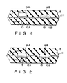
- Fig. 1 is a conventional IC device using a normal flat plate-like lead frame.
- reference numeral 11 denotes a lead frame.
- Two islands 12A and 12B are formed on the lead frame 11.
- Semiconductor chips 14A and 14B are respectively mounted on the islands 12A and 12B through an adhesive 13.
- Reference numeral 15 denotes a package made of a molding plastic. Note that, in Fig. 1, a metal thin wire connected by a bonding method is omitted.
- Fig. 2 shows a conventional IC device using an depressed type or island down type lead frame.
- reference numeral 11 denotes a lead frame; 12A and 12B, islands; 13, an adhesive; 14A and 14B, semiconductor chips; and 15, a package.
- thermo-compression bonding method Connection between each pad on a semiconductor chip and the corresponding lead by a thermo-compression bonding method or an ultrasonic thermo-compression bonding method is performed in the following manner.
- Each metal thin wire held by a bonder serving as a bonding device is compressed and thermally bonded on, e.g., the corresponding pad at the end of a tool at a predetermined temperature in a predetermined atmosphere, and the tool is moved along a predetermined track on the lead to bond the line to the lead by wedge bonding.
- a loop-like metal thin wire is connected between both the thermal bonding points.
- a mounting surface of each island is arranged to be uniformly lower than the upper surface of a lead by 0.15 mm to 0.2 mm.
- a package having predetermined outer dimensions is formed through a plastic molding step by a transfer molding method.
- a pair of upper and lower metal molds are set on a plastic molding device, a lead frame is stored in a cavity formed in the lower metal mold, and a molten molding plastic is flowed inside the cavity.
- Arrows in Figs. 1 and 2 represent paths along which the molten molding plastic flows in the cavity.
- This unsatisfactory filling of plastic causes not only degradation of an outer appearance of the package but formation of a void inside the package.
- the void generates a thermal stress and causes to disconnect the metal thin wires bonded by the thermal bonding method.
- the void allows entrance of moisture to degrade a moisture resistance.
- the unsatisfactory filling of the plastic causes degradation of reliability of a semiconductor device.
- a highly reliable plastic molded type semiconductor device which has a plurality of islands on which semiconductor chips are mounted and mounting surfaces of the islands lower than the upper surface of leads, wherein, when semiconductor chips having different substrate thicknesses are mounted on the islands, unsatisfactory filling of a molding plastic or formation of voids in a molding plastic constituting a package do not occur.
- a plastic molded type semiconductor device comprising a flat plate-like lead frame made of a conductive metal, a plurality of islands a surface of each of which is lowered from that of the lead frame by a predetermined amount upon bending of one part of the lead frame so as to lower the plurality of islands from the other part of the lead frame, a plurality of semiconductor chips respectively mounted on the plurality of islands and constituted by semiconductor substrates each having a predetermined thickness, and a package for burying and molding the semiconductor chips and made of a plastic material, wherein a lowering amount of the surface of each island from the lead frame is determined in accordance with a thickness of the substrate of each semiconductor chip.
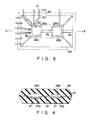
- Fig. 3 is a plan view showing an arrangement of a semiconductor device according to the first embodiment of the present invention in which a plastic molded type semiconductor device according to the present invention is applied to a QFP (Quad Flat Package) type IC device.
- QFP Quad Flat Package
- a boundary of a package made of a plastic is represented by an alternate long and short dashed line
- Fig. 4 is a sectional view showing the device taken along a line A - A′ in Fig. 3.
- reference numeral 21 denotes a lead frame obtained by punching or photoetching a metal thin plate made of iron, an alloy of iron and nickel, copper, or an alloy of copper.
- the lead frame is constituted by a plurality of leads 24 having a plurality of inner leads 22 the distal ends of which are free ends and outer leads 23 formed integrally with the inner leads 22, and two islands 25A and 25B for mounting semiconductor chips such as semiconductor integrated circuit chips.
- the islands 25A and 25B are formed near the free ends of the inner leads 22.
- the two islands 25A and 25B are connected to each other by a connecting portion 26.
- the connecting portion 26 is bent and formed to arrange a mounting surface of each semiconductor chip at a level lower than the upper surface of each of the plurality of leads 24.
- Two semiconductor chips such as semiconductor integrated circuit chips 28A and 28B are respectively mounted and fixed on the two islands 25A and 25B by an adhesive 27.
- the resultant structure is molded by a package 29 made of an insulating resin such as an epoxy-based resin material.
- the chips 28A and 28B can be obtained by forming an impurity region of an opposite conductivity type on, e.g., a silicon semiconductor substrate of a given conductivity type according to a known method and b forming electrodes or wirings connected to the impurity region and made of a conductive metal.
- the chips 28A and 28B are made of silicon semiconductor substrates having different thicknesses in accordance with characteristics of the chips. For example, each thickness falls within the range of 130 ⁇ m to 400 ⁇ m.
- adjustment for lowering the surface of an island can be performed in accordance with the thickness of the semiconductor chip, which is a characteristic feature of the present invention. That is, the surface of the island 25A on which the semiconductor integrated circuit chip 28A having a relatively large thickness is mounted is lowered by a large amount, and the surface of the island 25B on which the semiconductor integrated circuit chip 28B having a relatively small thickness is mounted is lowered by a small amount.
- a plastic molding step for forming the package 29 is performed in the following manner. For example, an insulating plastic tablet of an epoxy-based resin stored in a pot of a special-purpose molding device is compressed and melted through a cull and a runner, and the molten plastic flows through the gate of a cavity formed by a lower metal mold which stores a semiconductor chip.
- the thickness of the plastic package, i.e., a plastic molding layer is set to be smaller than 1.5 mm for surface mounting preparation as described above.
- Electrodes or bonding pads made of a conductive metal and formed on the semiconductor chip are electrically connected to the inner leads by an ultrasonic wire bonding step or a wire bonding step performed using a metal thin wire before the plastic molding step.
- the metal thin wire is illustrated by reference numeral 30 in Fig. 3.
- a loop of the metal thin wire is formed to have a height of about 300 ⁇ m.
- the metal thin wire having a diameter of about 50 ⁇ m and made of gold. copper. or aluminum is generally used.
- a lead frame made of copper or an alloy of copper must be used.
- a thermally bonding step is performed in an inert atmosphere, and it must be considered to prevent oxidation of the copper thin wire and the aluminum thin wire.
- the island Since a lowering amount of the surface of the island is naturally limited by the formation of the loop having a height of 300 ⁇ m in the thermally bonding step and the thickness of 1.5 mm, of the plastic molding layer for surface mounting preparation, the island must have a minimum thickness of 100 ⁇ m from the surface to serve as a material having moisture resistance or a protective material. Therefore, the lowering amount of the surface of the island falls within the range of 0.2 mm.
- a plastic molded semiconductor chip is ejected by an ejector pin arranged in a special-purpose device to separate the package from the molds, and a mark formed on the end surface of the ejector pin is embossed in the package.
- the present invention is not limited to the above embodiment, and various modifications can be performed.
- the case wherein two islands are provided has been described.
- the number of islands is not limited to two, and three or more islands may be provided.
- Fig. 5 is a plan view showing an arrangement of a plastic molded type semiconductor device according to the second embodiment of the present invention. Note that a boundary of a package 29 made of a plastic is represented by an alternate long and two short dashed line.
- Fig. 6 is a sectional view showing the device taken along a line B - B′ in Fig. 5. A different portion between the device of this embodiment and the device of the above embodiment shown in Figs. 3 and 4 is that a connecting portion 26 for connecting two islands 25A and 25B is cut in a half way. Therefore, the same reference numerals in Figs. 5 and 6 denote the same parts as in Figs. 3 and 4, and a detailed description thereof will be omitted.
Landscapes
- Structures Or Materials For Encapsulating Or Coating Semiconductor Devices Or Solid State Devices (AREA)
- Lead Frames For Integrated Circuits (AREA)
- Encapsulation Of And Coatings For Semiconductor Or Solid State Devices (AREA)
Applications Claiming Priority (2)
| Application Number | Priority Date | Filing Date | Title |
|---|---|---|---|
| JP185623/89 | 1989-07-18 | ||
| JP1185623A JPH0350758A (ja) | 1989-07-18 | 1989-07-18 | 樹脂封止型半導体装置 |
Publications (3)
| Publication Number | Publication Date |
|---|---|
| EP0409196A2 true EP0409196A2 (fr) | 1991-01-23 |
| EP0409196A3 EP0409196A3 (en) | 1992-05-06 |
| EP0409196B1 EP0409196B1 (fr) | 1996-03-13 |
Family
ID=16174031
Family Applications (1)
| Application Number | Title | Priority Date | Filing Date |
|---|---|---|---|
| EP90113767A Expired - Lifetime EP0409196B1 (fr) | 1989-07-18 | 1990-07-18 | Dispositif semi-conducteur du type à encapsulation en plastique |
Country Status (6)
| Country | Link |
|---|---|
| US (1) | US5049977A (fr) |
| EP (1) | EP0409196B1 (fr) |
| JP (1) | JPH0350758A (fr) |
| KR (1) | KR930004246B1 (fr) |
| DE (1) | DE69025815T2 (fr) |
| MY (1) | MY106727A (fr) |
Cited By (8)
| Publication number | Priority date | Publication date | Assignee | Title |
|---|---|---|---|---|
| EP0498446A3 (en) * | 1991-02-08 | 1993-10-20 | Toshiba Kk | Multichip packaged semiconductor device and method for manufacturing the same |
| EP0566921A1 (fr) * | 1992-04-18 | 1993-10-27 | TEMIC TELEFUNKEN microelectronic GmbH | Assemblage à semi-conducteurs, en particulier un module télécommande-récepteur |
| EP0774782A3 (fr) * | 1995-11-15 | 2000-02-23 | Mitsubishi Denki Kabushiki Kaisha | Module semi-conducteur de puissance |
| EP1187201A1 (fr) * | 2000-09-06 | 2002-03-13 | STMicroelectronics S.r.l. | Module multipuce |
| WO2004012485A3 (fr) * | 2002-07-31 | 2004-04-08 | Motorola Inc | Surfaces de montage pour dispositifs electroniques |
| SG109435A1 (en) * | 2000-12-07 | 2005-03-30 | Chuen Khiang Wang | Leaded mcm package and method therefor |
| US6927482B1 (en) * | 2003-10-01 | 2005-08-09 | General Electric Company | Surface mount package and method for forming multi-chip microsensor device |
| US7012324B2 (en) | 2003-09-12 | 2006-03-14 | Freescale Semiconductor, Inc. | Lead frame with flag support structure |
Families Citing this family (20)
| Publication number | Priority date | Publication date | Assignee | Title |
|---|---|---|---|---|
| US5349136A (en) * | 1989-08-02 | 1994-09-20 | Matsushita Electric Industrial Co., Ltd. | Mold tool assembly |
| EP0468379B1 (fr) * | 1990-07-21 | 1999-11-17 | Mitsui Chemicals, Inc. | Dispositif semi-conducteur comprenant un empaquetage |
| US5245216A (en) * | 1990-09-11 | 1993-09-14 | Kabushiki Kaisha Toshiba | Plastic-molded type semiconductor device |
| JPH04179263A (ja) * | 1990-11-14 | 1992-06-25 | Hitachi Ltd | 樹脂封止型半導体装置とその製造方法 |
| JP2708320B2 (ja) * | 1992-04-17 | 1998-02-04 | 三菱電機株式会社 | マルチチップ型半導体装置及びその製造方法 |
| JP3226244B2 (ja) * | 1993-12-03 | 2001-11-05 | 株式会社東芝 | 樹脂封止型半導体装置 |
| US5408126A (en) * | 1993-12-17 | 1995-04-18 | At&T Corp. | Manufacture of semiconductor devices and novel lead frame assembly |
| JP2806328B2 (ja) * | 1995-10-31 | 1998-09-30 | 日本電気株式会社 | 樹脂封止型半導体装置およびその製造方法 |
| DE19808193B4 (de) * | 1998-02-27 | 2007-11-08 | Robert Bosch Gmbh | Leadframevorrichtung und entsprechendes Herstellungsverfahren |
| US6081031A (en) * | 1998-06-29 | 2000-06-27 | Semiconductor Components Industries, Llc | Semiconductor package consisting of multiple conductive layers |
| SG109436A1 (en) * | 2000-12-07 | 2005-03-30 | Fung Leng Chen | Leaded mcm package and method therefor |
| US7053414B2 (en) * | 2004-04-12 | 2006-05-30 | Lite-On Technology Corporation | Optical semiconductor component to prevent electric leakage and provide different driving voltages |
| JP2006093238A (ja) * | 2004-09-21 | 2006-04-06 | Fuji Xerox Co Ltd | 半導体集積回路、半導体集積回路配置装置及び方法 |
| JP4895692B2 (ja) * | 2006-06-06 | 2012-03-14 | シャープ株式会社 | 電気機器及び導電体 |
| DE112006004098B4 (de) * | 2006-11-06 | 2013-01-31 | Infineon Technologies Ag | Halbleiter-Baugruppe mit einer Lead-Frame-Anordnung mit mindestens zwei Halbleiterchips und Verfahren zu deren Herstellung |
| TWI389283B (zh) * | 2007-10-22 | 2013-03-11 | 亞德諾公司 | 具有絕緣墊片以減少元件間漏電之封裝微晶片 |
| JP2010199492A (ja) * | 2009-02-27 | 2010-09-09 | Sanyo Electric Co Ltd | 半導体装置およびその製造方法 |
| US8951847B2 (en) | 2012-01-18 | 2015-02-10 | Intersil Americas LLC | Package leadframe for dual side assembly |
| US9387613B2 (en) | 2014-05-23 | 2016-07-12 | Infineon Technologies Ag | Semiconductor formation arrangement |
| JP6624065B2 (ja) | 2014-11-18 | 2019-12-25 | 日立化成株式会社 | 半導体装置及びその製造方法、並びに可撓性樹脂層形成用樹脂組成物 |
Family Cites Families (4)
| Publication number | Priority date | Publication date | Assignee | Title |
|---|---|---|---|---|
| JPS61259550A (ja) * | 1985-05-14 | 1986-11-17 | Toshiba Corp | 樹脂封止型半導体装置 |
| JPS6331149A (ja) * | 1986-07-25 | 1988-02-09 | Fujitsu Ltd | 半導体装置 |
| US4855807A (en) * | 1986-12-26 | 1989-08-08 | Kabushiki Kaisha Toshiba | Semiconductor device |
| US4800419A (en) * | 1987-01-28 | 1989-01-24 | Lsi Logic Corporation | Support assembly for integrated circuits |
-
1989
- 1989-07-18 JP JP1185623A patent/JPH0350758A/ja active Pending
-
1990
- 1990-07-12 US US07/551,442 patent/US5049977A/en not_active Expired - Lifetime
- 1990-07-14 MY MYPI90001184A patent/MY106727A/en unknown
- 1990-07-18 EP EP90113767A patent/EP0409196B1/fr not_active Expired - Lifetime
- 1990-07-18 KR KR1019900010862A patent/KR930004246B1/ko not_active Expired - Fee Related
- 1990-07-18 DE DE69025815T patent/DE69025815T2/de not_active Expired - Fee Related
Cited By (9)
| Publication number | Priority date | Publication date | Assignee | Title |
|---|---|---|---|---|
| EP0498446A3 (en) * | 1991-02-08 | 1993-10-20 | Toshiba Kk | Multichip packaged semiconductor device and method for manufacturing the same |
| EP0566921A1 (fr) * | 1992-04-18 | 1993-10-27 | TEMIC TELEFUNKEN microelectronic GmbH | Assemblage à semi-conducteurs, en particulier un module télécommande-récepteur |
| EP0774782A3 (fr) * | 1995-11-15 | 2000-02-23 | Mitsubishi Denki Kabushiki Kaisha | Module semi-conducteur de puissance |
| EP1187201A1 (fr) * | 2000-09-06 | 2002-03-13 | STMicroelectronics S.r.l. | Module multipuce |
| SG109435A1 (en) * | 2000-12-07 | 2005-03-30 | Chuen Khiang Wang | Leaded mcm package and method therefor |
| WO2004012485A3 (fr) * | 2002-07-31 | 2004-04-08 | Motorola Inc | Surfaces de montage pour dispositifs electroniques |
| US6996897B2 (en) | 2002-07-31 | 2006-02-14 | Freescale Semiconductor, Inc. | Method of making a mount for electronic devices |
| US7012324B2 (en) | 2003-09-12 | 2006-03-14 | Freescale Semiconductor, Inc. | Lead frame with flag support structure |
| US6927482B1 (en) * | 2003-10-01 | 2005-08-09 | General Electric Company | Surface mount package and method for forming multi-chip microsensor device |
Also Published As
| Publication number | Publication date |
|---|---|
| US5049977A (en) | 1991-09-17 |
| DE69025815D1 (de) | 1996-04-18 |
| EP0409196A3 (en) | 1992-05-06 |
| EP0409196B1 (fr) | 1996-03-13 |
| JPH0350758A (ja) | 1991-03-05 |
| KR930004246B1 (ko) | 1993-05-22 |
| DE69025815T2 (de) | 1996-08-08 |
| KR910003791A (ko) | 1991-02-28 |
| MY106727A (en) | 1995-07-31 |
Similar Documents
| Publication | Publication Date | Title |
|---|---|---|
| EP0409196B1 (fr) | Dispositif semi-conducteur du type à encapsulation en plastique | |
| US6117710A (en) | Plastic package with exposed die and method of making same | |
| US7507606B2 (en) | Semiconductor device and method of manufacturing the same | |
| KR100703830B1 (ko) | 수지밀봉형 반도체장치의 제조방법 | |
| CA1252912A (fr) | Boitier de dispositif a semiconducteur a connexions d'entree-sortie nombreuses | |
| US5834831A (en) | Semiconductor device with improved heat dissipation efficiency | |
| US5198964A (en) | Packaged semiconductor device and electronic device module including same | |
| US6291274B1 (en) | Resin molded semiconductor device and method for manufacturing the same | |
| US5818105A (en) | Semiconductor device with plastic material covering a semiconductor chip mounted on a substrate of the device | |
| US6861734B2 (en) | Resin-molded semiconductor device | |
| US6553657B2 (en) | Semiconductor device | |
| US20030011054A1 (en) | Power module package having improved heat dissipating capability | |
| US6593169B2 (en) | Method of making hybrid integrated circuit device | |
| KR101532443B1 (ko) | Qfn 패키지를 위한 방법 및 장치 | |
| JPH0730046A (ja) | 半導体装置、リードフレーム及び半導体装置の製造方法 | |
| US5929513A (en) | Semiconductor device and heat sink used therein | |
| JP2001313363A (ja) | 樹脂封止型半導体装置 | |
| CN100463169C (zh) | 混合集成电路装置及其制造方法 | |
| JP3375224B2 (ja) | 半導体装置及びその製造方法 | |
| US6075281A (en) | Modified lead finger for wire bonding | |
| US20040262752A1 (en) | Semiconductor device | |
| JPH07161876A (ja) | 半導体集積回路装置およびその製造方法ならびにその製造に用いるモールド金型 | |
| US6268644B1 (en) | Semiconductor device | |
| US6105245A (en) | Method of manufacturing a resin-encapsulated semiconductor package | |
| JP2002076231A (ja) | リードフレーム、成形金型、及び半導体装置 |
Legal Events
| Date | Code | Title | Description |
|---|---|---|---|
| PUAI | Public reference made under article 153(3) epc to a published international application that has entered the european phase |
Free format text: ORIGINAL CODE: 0009012 |
|
| 17P | Request for examination filed |
Effective date: 19900718 |
|
| AK | Designated contracting states |
Kind code of ref document: A2 Designated state(s): DE FR GB |
|
| PUAL | Search report despatched |
Free format text: ORIGINAL CODE: 0009013 |
|
| AK | Designated contracting states |
Kind code of ref document: A3 Designated state(s): DE FR GB |
|
| 17Q | First examination report despatched |
Effective date: 19940802 |
|
| GRAA | (expected) grant |
Free format text: ORIGINAL CODE: 0009210 |
|
| AK | Designated contracting states |
Kind code of ref document: B1 Designated state(s): DE FR GB |
|
| REF | Corresponds to: |
Ref document number: 69025815 Country of ref document: DE Date of ref document: 19960418 |
|
| ET | Fr: translation filed | ||
| GRAH | Despatch of communication of intention to grant a patent |
Free format text: ORIGINAL CODE: EPIDOS IGRA |
|
| PLBE | No opposition filed within time limit |
Free format text: ORIGINAL CODE: 0009261 |
|
| STAA | Information on the status of an ep patent application or granted ep patent |
Free format text: STATUS: NO OPPOSITION FILED WITHIN TIME LIMIT |
|
| 26N | No opposition filed | ||
| PGFP | Annual fee paid to national office [announced via postgrant information from national office to epo] |
Ref country code: GB Payment date: 19970709 Year of fee payment: 8 |
|
| PGFP | Annual fee paid to national office [announced via postgrant information from national office to epo] |
Ref country code: DE Payment date: 19970725 Year of fee payment: 8 |
|
| PG25 | Lapsed in a contracting state [announced via postgrant information from national office to epo] |
Ref country code: GB Free format text: LAPSE BECAUSE OF NON-PAYMENT OF DUE FEES Effective date: 19980718 |
|
| GBPC | Gb: european patent ceased through non-payment of renewal fee |
Effective date: 19980718 |
|
| REG | Reference to a national code |
Ref country code: FR Ref legal event code: D6 |
|
| PG25 | Lapsed in a contracting state [announced via postgrant information from national office to epo] |
Ref country code: DE Free format text: LAPSE BECAUSE OF NON-PAYMENT OF DUE FEES Effective date: 19990501 |
|
| PGFP | Annual fee paid to national office [announced via postgrant information from national office to epo] |
Ref country code: FR Payment date: 20070710 Year of fee payment: 18 |
|
| REG | Reference to a national code |
Ref country code: FR Ref legal event code: ST Effective date: 20090331 |
|
| PG25 | Lapsed in a contracting state [announced via postgrant information from national office to epo] |
Ref country code: FR Free format text: LAPSE BECAUSE OF NON-PAYMENT OF DUE FEES Effective date: 20080731 |