EP0416573A1 - Harzvergossener Halbleiterbauteil mit Aussenanschlüssen gestaltet für Multifunktionen - Google Patents
Harzvergossener Halbleiterbauteil mit Aussenanschlüssen gestaltet für Multifunktionen Download PDFInfo
- Publication number
- EP0416573A1 EP0416573A1 EP19900117063 EP90117063A EP0416573A1 EP 0416573 A1 EP0416573 A1 EP 0416573A1 EP 19900117063 EP19900117063 EP 19900117063 EP 90117063 A EP90117063 A EP 90117063A EP 0416573 A1 EP0416573 A1 EP 0416573A1
- Authority
- EP
- European Patent Office
- Prior art keywords
- leads
- type semiconductor
- resin sealing
- pitches
- outer leads
- Prior art date
- Legal status (The legal status is an assumption and is not a legal conclusion. Google has not performed a legal analysis and makes no representation as to the accuracy of the status listed.)
- Granted
Links
Images


Classifications
-
- H—ELECTRICITY
- H10—SEMICONDUCTOR DEVICES; ELECTRIC SOLID-STATE DEVICES NOT OTHERWISE PROVIDED FOR
- H10W—GENERIC PACKAGES, INTERCONNECTIONS, CONNECTORS OR OTHER CONSTRUCTIONAL DETAILS OF DEVICES COVERED BY CLASS H10
- H10W74/00—Encapsulations, e.g. protective coatings
- H10W74/10—Encapsulations, e.g. protective coatings characterised by their shape or disposition
-
- H—ELECTRICITY
- H10—SEMICONDUCTOR DEVICES; ELECTRIC SOLID-STATE DEVICES NOT OTHERWISE PROVIDED FOR
- H10W—GENERIC PACKAGES, INTERCONNECTIONS, CONNECTORS OR OTHER CONSTRUCTIONAL DETAILS OF DEVICES COVERED BY CLASS H10
- H10W90/00—Package configurations
- H10W90/811—Multiple chips on leadframes
-
- H—ELECTRICITY
- H10—SEMICONDUCTOR DEVICES; ELECTRIC SOLID-STATE DEVICES NOT OTHERWISE PROVIDED FOR
- H10W—GENERIC PACKAGES, INTERCONNECTIONS, CONNECTORS OR OTHER CONSTRUCTIONAL DETAILS OF DEVICES COVERED BY CLASS H10
- H10W72/00—Interconnections or connectors in packages
- H10W72/50—Bond wires
- H10W72/541—Dispositions of bond wires
- H10W72/5449—Dispositions of bond wires not being orthogonal to a side surface of the chip, e.g. fan-out arrangements
-
- H—ELECTRICITY
- H10—SEMICONDUCTOR DEVICES; ELECTRIC SOLID-STATE DEVICES NOT OTHERWISE PROVIDED FOR
- H10W—GENERIC PACKAGES, INTERCONNECTIONS, CONNECTORS OR OTHER CONSTRUCTIONAL DETAILS OF DEVICES COVERED BY CLASS H10
- H10W72/00—Interconnections or connectors in packages
- H10W72/50—Bond wires
- H10W72/551—Materials of bond wires
- H10W72/552—Materials of bond wires comprising metals or metalloids, e.g. silver
- H10W72/5522—Materials of bond wires comprising metals or metalloids, e.g. silver comprising gold [Au]
-
- H—ELECTRICITY
- H10—SEMICONDUCTOR DEVICES; ELECTRIC SOLID-STATE DEVICES NOT OTHERWISE PROVIDED FOR
- H10W—GENERIC PACKAGES, INTERCONNECTIONS, CONNECTORS OR OTHER CONSTRUCTIONAL DETAILS OF DEVICES COVERED BY CLASS H10
- H10W72/00—Interconnections or connectors in packages
- H10W72/50—Bond wires
- H10W72/551—Materials of bond wires
- H10W72/552—Materials of bond wires comprising metals or metalloids, e.g. silver
- H10W72/5525—Materials of bond wires comprising metals or metalloids, e.g. silver comprising copper [Cu]
-
- H—ELECTRICITY
- H10—SEMICONDUCTOR DEVICES; ELECTRIC SOLID-STATE DEVICES NOT OTHERWISE PROVIDED FOR
- H10W—GENERIC PACKAGES, INTERCONNECTIONS, CONNECTORS OR OTHER CONSTRUCTIONAL DETAILS OF DEVICES COVERED BY CLASS H10
- H10W72/00—Interconnections or connectors in packages
- H10W72/90—Bond pads, in general
- H10W72/921—Structures or relative sizes of bond pads
- H10W72/926—Multiple bond pads having different sizes
-
- H—ELECTRICITY
- H10—SEMICONDUCTOR DEVICES; ELECTRIC SOLID-STATE DEVICES NOT OTHERWISE PROVIDED FOR
- H10W—GENERIC PACKAGES, INTERCONNECTIONS, CONNECTORS OR OTHER CONSTRUCTIONAL DETAILS OF DEVICES COVERED BY CLASS H10
- H10W74/00—Encapsulations, e.g. protective coatings
-
- H—ELECTRICITY
- H10—SEMICONDUCTOR DEVICES; ELECTRIC SOLID-STATE DEVICES NOT OTHERWISE PROVIDED FOR
- H10W—GENERIC PACKAGES, INTERCONNECTIONS, CONNECTORS OR OTHER CONSTRUCTIONAL DETAILS OF DEVICES COVERED BY CLASS H10
- H10W90/00—Package configurations
- H10W90/701—Package configurations characterised by the relative positions of pads or connectors relative to package parts
- H10W90/751—Package configurations characterised by the relative positions of pads or connectors relative to package parts of bond wires
- H10W90/756—Package configurations characterised by the relative positions of pads or connectors relative to package parts of bond wires between a chip and a stacked lead frame, conducting package substrate or heat sink
Definitions
- the present invention relates to a resin sealing type semiconductor apparatus in which a power transistor or power IC having large power or generating a large amount of heat at the time of operation is installed. More particularly, this invention relates to outer leads of a semiconductor apparatus.
- the dielectric strength should be considered.
- a typical measure against the dielectric strength is to increase the pitches between the outer leads while making the pitches the same.
- Figs. 1 through 5B exemplifies the above three prior arts.
- Fig. 1 is a perspective view of a photocoupler which performs a zero cross function and has three different pitches, the smallest, reference pitch P and its integer-multiple pitches 2P and 4P between outer leads 2 led out from a sealing resin layer 1.
- Fig. 2 exemplifies a type having two pitches, P and 2P, between outer leads 2 which are characterized in that their free ends have a smaller diameter.
- Figs. 3 to 5B illustrate other examples.
- a resin sealing type semiconductor apparatus requires that the pitches between outer leads be increased in light of the dielectric strength necessary for the power element installed in the package and that the pitches between outer leads of other semiconductor apparatuses constituting a power element control section should also be increased. Further, with an SIP type lead frame in use, the outer leads are led out from one direction.
- the number of outer leads and the pitches between the leads are restricted by the size of the package, thus hindering realization of multi-functions (multi-pins) of the resin sealing type semiconductor apparatus.
- mounted semiconductor devices are supported by the inner leads alone.
- the leads may deform during assembling of the apparatus.
- a resin sealing type semiconductor apparatus comprising: semiconductor devices each having electrodes; a plurality of leads including inner leads and outer leads, the inner leads being connected to the electrodes of the semiconductor devices; and a sealing resin layer for sealing at least the semiconductor devices and the inner leads, the outer leads being led out in one direction from the sealing resin layer and having two or more types of pitches therebetween, each type having two or more pitches.
- a module product is provided by installing on a printed circuit board a resin sealing type semiconductor apparatus which has electronic parts, including a power element that needs a dielectric strength, mounted on its lead frame. Since the size of the printed circuit board is determined by a machine in use, the printed circuit board is assumed to have a specific area. Accordingly, it is necessary to select the lead frame used in assembling a resin sealing type semiconductor apparatus in light of the mounting or package density on the printed circuit board having a specific area.
- a resin sealing type semiconductor apparatus according to the present invention employs an SIP type lead frame which has outer leads led out in one direction from a sealing resin layer for the following reason.
- the outer leads mounted on the surface of the printed circuit board are fitted in through holes formed in row on the printed circuit board, so that the plane area can be reduced as compared with the one utilizing a DIP (Dual In Line Package) type lead frame.
- the resin sealing type semiconductor apparatus according to the present invention is designed to allow a power element besides a control IC to be mounted.
- a resin sealing type semiconductor apparatus embodying the present invention electronic circuits including a power element that should have a dielectric strength are constituted in an assembling step utilizing a lead frame.
- a module product is provided by a mounting system that mounts outer leads, led out from a package made of a sealing resin, on a printed circuit board.
- a so-called SIP type lead frame is used, which will be described below. It is typical to form a lead frame having a specific pattern by subjecting a copper or copper alloy plate to a stamping process. The stamping process is not, however, essential, and may be replaced with an etching step.
- the SIP type lead frame a plurality of inner leads are provided on the frame, and beds are formed on free ends of some of the inner leads.
- through holes 11 are formed in a metal frame 10 to receive alignment pins (not shown) at the time the lead frame is conveyed, and inner leads 15 and 15a are formed relatively wider to improve the mechanical strength as well as the current capacity and heat-generating performance.
- the inner lead 15a is connected to a bed 13 having a relatively large area, and a power element 17, such as a Darlington transistor, is mounted on the bed 13.
- the free ends of the thinnest inner leads 15 are collected to be floating ends at the proximity of a bed 14 which has a smaller area than the bed 13 and on which, for example, a control IC 18 is to be mounted.
- electrodes 20 formed on the semiconductor devices are electrically connected to the inner leads 15 by means of thin metal wires 19 made of a metal selected from a group of gold, Al and copper (copper alloy allowable).
- the electrical connection is made by, for example, well-known wire ball bonding method or ultrasonic bonding method by which the electrodes 20 and inner leads 15 are connected by the thin metal wires 19 made to form predetermined loci and form loops of predetermined heights.
- a lead frame made of copper or copper alloy having a high thermal conductance is preferable for the power element 17 that generates a large amount of heat, and the lead frame has a thickness of 0.4 to 0.8 mm.
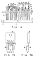
- the inner lead 15a for supporting the bed 13 on which the power element 17 is to be mounted is formed to have a width 2l (e.g., 2 mm) nearly double the width l of the other inner leads 15, and those of the outer leads 12 which have the pitch of 1.27 mm are formed in a zigzag to be fitted in the through holes formed in the printed circuit board or be mounted thereon.
- Two outer leads 12 with the pitch 2P are provided in Fig. 7A, whereas two or more outer leads 12 with the pitches P and 2P are provided in Fig. 8A.
- Figs. 7A, 7B, 8A and 8B illustrate packages acquired through a resin sealing step conducted by the well-known transfer mold method after the above mounting step is completed.
- Figs. 7A and 8A are front views, and Figs. 7B and 8B side views.
- the illustrated packages are the products after removing the unnecessary lead frame portion, forming the outer leads and checking bending of leads.
- Figs. 7A to 8B each illustrate a package having the outer leads 12 led out in one direction from the sealing resin layer 16, omitting a plurality of beds shown in Fig. 6; actually, the power element 17 that generates a large amount of heat is mounted on the bed 13.
- Such a resin sealing type semiconductor apparatus has a combination of a power element 17 and a control IC 18, and can be applied to a module product as a semiconductor apparatus with a small area.
- This resin sealing type semiconductor apparatus can therefore easily be mounted on the printed circuit board.
- the width of the inner leads that support beds on which power elements are to be mounted are increased to prevent deformation of the apparatus, the yield in the fabricating process is improved and the resultant resin sealing type semiconductor apparatus has an excellent heat-generating performance.
Landscapes
- Lead Frames For Integrated Circuits (AREA)
- Structures Or Materials For Encapsulating Or Coating Semiconductor Devices Or Solid State Devices (AREA)
Applications Claiming Priority (2)
| Application Number | Priority Date | Filing Date | Title |
|---|---|---|---|
| JP230070/89 | 1989-09-05 | ||
| JP23007089A JP2515406B2 (ja) | 1989-09-05 | 1989-09-05 | 樹脂封止型半導体装置 |
Publications (2)
| Publication Number | Publication Date |
|---|---|
| EP0416573A1 true EP0416573A1 (de) | 1991-03-13 |
| EP0416573B1 EP0416573B1 (de) | 1999-05-19 |
Family
ID=16902072
Family Applications (1)
| Application Number | Title | Priority Date | Filing Date |
|---|---|---|---|
| EP19900117063 Expired - Lifetime EP0416573B1 (de) | 1989-09-05 | 1990-09-05 | Harzvergossener Halbleiterbauteil mit Aussenanschlüssen gestaltet für Multifunktionen |
Country Status (4)
| Country | Link |
|---|---|
| US (1) | US5031024A (de) |
| EP (1) | EP0416573B1 (de) |
| JP (1) | JP2515406B2 (de) |
| KR (1) | KR930004255B1 (de) |
Families Citing this family (7)
| Publication number | Priority date | Publication date | Assignee | Title |
|---|---|---|---|---|
| CN1312767C (zh) * | 2001-05-18 | 2007-04-25 | 三洋电机株式会社 | 电源电路装置 |
| JP4651652B2 (ja) * | 2001-05-18 | 2011-03-16 | 三洋電機株式会社 | 電源回路装置 |
| JP3812447B2 (ja) * | 2002-01-28 | 2006-08-23 | 富士電機デバイステクノロジー株式会社 | 樹脂封止形半導体装置 |
| JP3872001B2 (ja) * | 2002-11-18 | 2007-01-24 | シャープ株式会社 | リードフレーム、それを用いた半導体装置の製造方法、それを用いた半導体装置、及び電子機器 |
| DE102008040565B4 (de) * | 2008-07-21 | 2024-01-11 | Robert Bosch Gmbh | Gehäuse für ein Halbleiterbauelement |
| US9035437B2 (en) * | 2013-03-12 | 2015-05-19 | Infineon Technologies Austria Ag | Packaged device comprising non-integer lead pitches and method of manufacturing the same |
| WO2022118288A1 (en) * | 2020-12-04 | 2022-06-09 | Molex, Llc | High-power electronics devices and methods for manufacturing same |
Citations (6)
| Publication number | Priority date | Publication date | Assignee | Title |
|---|---|---|---|---|
| GB2115607A (en) * | 1982-02-05 | 1983-09-07 | Hitachi Ltd | Semiconductor device and a method of producing the same |
| JPS5933838A (ja) * | 1982-08-19 | 1984-02-23 | Toshiba Corp | 半導体樹脂封止用金型装置 |
| JPS59115551A (ja) * | 1982-12-22 | 1984-07-04 | Toshiba Corp | 半導体装置 |
| US4697203A (en) * | 1984-06-04 | 1987-09-29 | Mitsubishi Denki Kabushiki Kaisha | Semiconductor device and manufacturing method therefor |
| EP0258098A1 (de) * | 1986-07-25 | 1988-03-02 | Fujitsu Limited | Verkapselte Halbleiteranordnung und Verfahren zu deren Herstellung |
| JPS63318131A (ja) * | 1987-06-22 | 1988-12-27 | Oki Electric Ind Co Ltd | 硬化樹脂による樹脂封止方法 |
Family Cites Families (4)
| Publication number | Priority date | Publication date | Assignee | Title |
|---|---|---|---|---|
| JPS60107848A (ja) * | 1983-11-16 | 1985-06-13 | Hitachi Ltd | 半導体装置およびこれに用いられるリ−ドフレ−ム |
| JPS6132452A (ja) * | 1984-07-25 | 1986-02-15 | Hitachi Ltd | リ−ドフレ−ムとそれを用いた電子装置 |
| JPH0451489Y2 (de) * | 1987-03-31 | 1992-12-03 | ||
| JPH01216565A (ja) * | 1988-02-25 | 1989-08-30 | Canon Inc | 電子部品 |
-
1989
- 1989-09-05 JP JP23007089A patent/JP2515406B2/ja not_active Expired - Fee Related
-
1990
- 1990-09-04 US US07/576,936 patent/US5031024A/en not_active Expired - Lifetime
- 1990-09-05 EP EP19900117063 patent/EP0416573B1/de not_active Expired - Lifetime
- 1990-09-05 KR KR1019900013981A patent/KR930004255B1/ko not_active Expired - Fee Related
Patent Citations (6)
| Publication number | Priority date | Publication date | Assignee | Title |
|---|---|---|---|---|
| GB2115607A (en) * | 1982-02-05 | 1983-09-07 | Hitachi Ltd | Semiconductor device and a method of producing the same |
| JPS5933838A (ja) * | 1982-08-19 | 1984-02-23 | Toshiba Corp | 半導体樹脂封止用金型装置 |
| JPS59115551A (ja) * | 1982-12-22 | 1984-07-04 | Toshiba Corp | 半導体装置 |
| US4697203A (en) * | 1984-06-04 | 1987-09-29 | Mitsubishi Denki Kabushiki Kaisha | Semiconductor device and manufacturing method therefor |
| EP0258098A1 (de) * | 1986-07-25 | 1988-03-02 | Fujitsu Limited | Verkapselte Halbleiteranordnung und Verfahren zu deren Herstellung |
| JPS63318131A (ja) * | 1987-06-22 | 1988-12-27 | Oki Electric Ind Co Ltd | 硬化樹脂による樹脂封止方法 |
Also Published As
| Publication number | Publication date |
|---|---|
| KR930004255B1 (ko) | 1993-05-22 |
| US5031024A (en) | 1991-07-09 |
| EP0416573B1 (de) | 1999-05-19 |
| JP2515406B2 (ja) | 1996-07-10 |
| KR910007117A (ko) | 1991-04-30 |
| JPH0393257A (ja) | 1991-04-18 |
Similar Documents
| Publication | Publication Date | Title |
|---|---|---|
| US5413970A (en) | Process for manufacturing a semiconductor package having two rows of interdigitated leads | |
| US6756663B2 (en) | Semiconductor device including wiring board with three dimensional wiring pattern | |
| EP2005470B1 (de) | Leiterrahmenbasiertes, umgossenes halbleitergehäuse mit integrierten durchgangsbohrungstechnologie-wärmeverteilerstiften und entsprechendes herstellungsverfahren | |
| US7160759B2 (en) | Semiconductor device and method of manufacturing the same | |
| US5747874A (en) | Semiconductor device, base member for semiconductor device and semiconductor device unit | |
| US6444905B1 (en) | Semiconductor device | |
| JPH09191060A (ja) | 集積回路のプラスチックパッケージング | |
| JPH06283650A (ja) | 半導体装置 | |
| US20090020859A1 (en) | Quad flat package with exposed common electrode bars | |
| US6780679B2 (en) | Semiconductor device and method of manufacturing the same | |
| US6642082B2 (en) | Method for manufacturing a resin-sealed semiconductor device | |
| US5233131A (en) | Integrated circuit die-to-leadframe interconnect assembly system | |
| CN1568543B (zh) | 半导体元件 | |
| EP0416573B1 (de) | Harzvergossener Halbleiterbauteil mit Aussenanschlüssen gestaltet für Multifunktionen | |
| US5196992A (en) | Resin sealing type semiconductor device in which a very small semiconductor chip is sealed in package with resin | |
| US5708295A (en) | Lead frame and method of manufacturing the same, and resin sealed semiconductor device and method of manufacturing the same | |
| US6181000B1 (en) | Lead frame for ball grid array, semiconductor device having it, and process for producing it | |
| EP0414257B1 (de) | Halbleiteranordnung des Harzverkapselungstyps, in dem ein sehr kleiner Halbleiterchip mit Harz versiegelt ist | |
| JPH10154768A (ja) | 半導体装置及びその製造方法 | |
| JPH07297236A (ja) | 半導体素子実装用フィルムと半導体素子実装構造 | |
| KR100487464B1 (ko) | 리드프레임을이용한반도체칩패키지 | |
| JP2534545B2 (ja) | 電子部品搭載用基板 | |
| JP3036597B1 (ja) | 半導体装置用リードフレーム | |
| KR100195511B1 (ko) | 리드 프레임을 이용한 볼 그리드 어레이 패키지 | |
| KR0177006B1 (ko) | 복합 리드 구성을 가진 반도체 장치 |
Legal Events
| Date | Code | Title | Description |
|---|---|---|---|
| PUAI | Public reference made under article 153(3) epc to a published international application that has entered the european phase |
Free format text: ORIGINAL CODE: 0009012 |
|
| 17P | Request for examination filed |
Effective date: 19900905 |
|
| AK | Designated contracting states |
Kind code of ref document: A1 Designated state(s): DE FR GB |
|
| 17Q | First examination report despatched |
Effective date: 19930608 |
|
| GRAG | Despatch of communication of intention to grant |
Free format text: ORIGINAL CODE: EPIDOS AGRA |
|
| GRAG | Despatch of communication of intention to grant |
Free format text: ORIGINAL CODE: EPIDOS AGRA |
|
| GRAH | Despatch of communication of intention to grant a patent |
Free format text: ORIGINAL CODE: EPIDOS IGRA |
|
| GRAH | Despatch of communication of intention to grant a patent |
Free format text: ORIGINAL CODE: EPIDOS IGRA |
|
| GRAA | (expected) grant |
Free format text: ORIGINAL CODE: 0009210 |
|
| AK | Designated contracting states |
Kind code of ref document: B1 Designated state(s): GB |
|
| RBV | Designated contracting states (corrected) |
Designated state(s): GB |
|
| PLBE | No opposition filed within time limit |
Free format text: ORIGINAL CODE: 0009261 |
|
| STAA | Information on the status of an ep patent application or granted ep patent |
Free format text: STATUS: NO OPPOSITION FILED WITHIN TIME LIMIT |
|
| 26N | No opposition filed | ||
| REG | Reference to a national code |
Ref country code: GB Ref legal event code: IF02 |
|
| PGFP | Annual fee paid to national office [announced via postgrant information from national office to epo] |
Ref country code: GB Payment date: 20050831 Year of fee payment: 16 |
|
| GBPC | Gb: european patent ceased through non-payment of renewal fee |
Effective date: 20060905 |
|
| PG25 | Lapsed in a contracting state [announced via postgrant information from national office to epo] |
Ref country code: GB Free format text: LAPSE BECAUSE OF NON-PAYMENT OF DUE FEES Effective date: 20060905 |