EP0418538A1 - Improvements in or relating to balun transformers - Google Patents
Improvements in or relating to balun transformers Download PDFInfo
- Publication number
- EP0418538A1 EP0418538A1 EP90115279A EP90115279A EP0418538A1 EP 0418538 A1 EP0418538 A1 EP 0418538A1 EP 90115279 A EP90115279 A EP 90115279A EP 90115279 A EP90115279 A EP 90115279A EP 0418538 A1 EP0418538 A1 EP 0418538A1
- Authority
- EP
- European Patent Office
- Prior art keywords
- balun
- conductor
- balanced
- ground
- conductor elements
- Prior art date
- Legal status (The legal status is an assumption and is not a legal conclusion. Google has not performed a legal analysis and makes no representation as to the accuracy of the status listed.)
- Granted
Links
Images

Classifications
-
- H—ELECTRICITY
- H01—ELECTRIC ELEMENTS
- H01P—WAVEGUIDES; RESONATORS, LINES, OR OTHER DEVICES OF THE WAVEGUIDE TYPE
- H01P5/00—Coupling devices of the waveguide type
- H01P5/08—Coupling devices of the waveguide type for linking dissimilar lines or devices
- H01P5/10—Coupling devices of the waveguide type for linking dissimilar lines or devices for coupling balanced lines or devices with unbalanced lines or devices
-
- H—ELECTRICITY
- H03—ELECTRONIC CIRCUITRY
- H03F—AMPLIFIERS
- H03F3/00—Amplifiers with only discharge tubes or only semiconductor devices as amplifying elements
- H03F3/20—Power amplifiers, e.g. Class B amplifiers, Class C amplifiers
- H03F3/21—Power amplifiers, e.g. Class B amplifiers, Class C amplifiers with semiconductor devices only
- H03F3/211—Power amplifiers, e.g. Class B amplifiers, Class C amplifiers with semiconductor devices only using a combination of several amplifiers
-
- H—ELECTRICITY
- H01—ELECTRIC ELEMENTS
- H01F—MAGNETS; INDUCTANCES; TRANSFORMERS; SELECTION OF MATERIALS FOR THEIR MAGNETIC PROPERTIES
- H01F27/00—Details of transformers or inductances, in general
- H01F27/28—Coils; Windings; Conductive connections
-
- H—ELECTRICITY
- H01—ELECTRIC ELEMENTS
- H01F—MAGNETS; INDUCTANCES; TRANSFORMERS; SELECTION OF MATERIALS FOR THEIR MAGNETIC PROPERTIES
- H01F27/00—Details of transformers or inductances, in general
- H01F27/28—Coils; Windings; Conductive connections
- H01F27/2804—Printed windings
-
- H—ELECTRICITY
- H03—ELECTRONIC CIRCUITRY
- H03F—AMPLIFIERS
- H03F3/00—Amplifiers with only discharge tubes or only semiconductor devices as amplifying elements
- H03F3/20—Power amplifiers, e.g. Class B amplifiers, Class C amplifiers
- H03F3/24—Power amplifiers, e.g. Class B amplifiers, Class C amplifiers of transmitter output stages
- H03F3/245—Power amplifiers, e.g. Class B amplifiers, Class C amplifiers of transmitter output stages with semiconductor devices only
-
- H—ELECTRICITY
- H05—ELECTRIC TECHNIQUES NOT OTHERWISE PROVIDED FOR
- H05K—PRINTED CIRCUITS; CASINGS OR CONSTRUCTIONAL DETAILS OF ELECTRIC APPARATUS; MANUFACTURE OF ASSEMBLAGES OF ELECTRICAL COMPONENTS
- H05K1/00—Printed circuits
- H05K1/16—Printed circuits incorporating printed electric components, e.g. printed resistors, capacitors or inductors
- H05K1/165—Printed circuits incorporating printed electric components, e.g. printed resistors, capacitors or inductors incorporating printed inductors
-
- H—ELECTRICITY
- H05—ELECTRIC TECHNIQUES NOT OTHERWISE PROVIDED FOR
- H05K—PRINTED CIRCUITS; CASINGS OR CONSTRUCTIONAL DETAILS OF ELECTRIC APPARATUS; MANUFACTURE OF ASSEMBLAGES OF ELECTRICAL COMPONENTS
- H05K1/00—Printed circuits
- H05K1/02—Details
- H05K1/0213—Electrical arrangements not otherwise provided for
- H05K1/0237—High frequency adaptations
-
- H—ELECTRICITY
- H05—ELECTRIC TECHNIQUES NOT OTHERWISE PROVIDED FOR
- H05K—PRINTED CIRCUITS; CASINGS OR CONSTRUCTIONAL DETAILS OF ELECTRIC APPARATUS; MANUFACTURE OF ASSEMBLAGES OF ELECTRICAL COMPONENTS
- H05K1/00—Printed circuits
- H05K1/18—Printed circuits structurally associated with non-printed electric components
- H05K1/182—Printed circuits structurally associated with non-printed electric components associated with components mounted in printed circuit boards [PCB], e.g. insert-mounted components [IMC]
-
- H—ELECTRICITY
- H05—ELECTRIC TECHNIQUES NOT OTHERWISE PROVIDED FOR
- H05K—PRINTED CIRCUITS; CASINGS OR CONSTRUCTIONAL DETAILS OF ELECTRIC APPARATUS; MANUFACTURE OF ASSEMBLAGES OF ELECTRICAL COMPONENTS
- H05K2201/00—Indexing scheme relating to printed circuits covered by H05K1/00
- H05K2201/10—Details of components or other objects attached to or integrated in a printed circuit board
- H05K2201/10007—Types of components
- H05K2201/10166—Transistor
-
- H—ELECTRICITY
- H05—ELECTRIC TECHNIQUES NOT OTHERWISE PROVIDED FOR
- H05K—PRINTED CIRCUITS; CASINGS OR CONSTRUCTIONAL DETAILS OF ELECTRIC APPARATUS; MANUFACTURE OF ASSEMBLAGES OF ELECTRICAL COMPONENTS
- H05K3/00—Apparatus or processes for manufacturing printed circuits
- H05K3/0058—Laminating printed circuit boards onto other substrates, e.g. metallic substrates
- H05K3/0061—Laminating printed circuit boards onto other substrates, e.g. metallic substrates onto a metallic substrate, e.g. a heat sink
Definitions
- the present invention relates to baluns, that is transformers capable of matching a single-ended output to a balanced input and vice versa.
- a balun consider a high power transistor amplifier. Where output power requirements exceed that which can be delivered by a single transistor, a plurality of transistors may be coupled to share the power demand.
- a base station of a cellular radio network for example, operating in the high frequency region of 900 MHz, an output power requirement at the antenna feed of 1 kwatt would be typical, delivered by ten 100 watt amplifier modules.
- the upper limit power capability of radio-frequency (r.f.) power transistors is in the region of 60 watt, hence to provide such a 100 watt module coupled transistors must be used.
- a convenient and useful method of coupling two transistors is the technique known in the art as "push-pull".
- the drive is shared between a transistor driving current through the load in one direction and a second transistor driving current through the load in the opposite direction.
- the arrangement is advantageous in terms of impedance matching, presenting a higher output impedance than the very low impedance of a single transistor or the yet lower impedance of parallel transistors, the higher output impedance being closer to the typical target impedance of 50, but unfortunately is inherently a balanced system, that is it produces an output signal which is symmetrical with respect to the common ground potential of the coupled transistors, whereas typically a single-ended (that is ground referenced) output signal is required.
- a solution to this problem is to provide a transformer between the output of the push-pull pair and the load. By virtue of its isolating properties, a transformer is able to couple the balanced output to the single-ended load. Such a transformer is that referred to in the art as a balun.
- balun may be used to covert such an unbalanced input to the balanced drive signals.
- balun including transmission line forms
- Examples have been described by C.L. Ruthroff in his paper “Some Broad-Band Transformers” (Proceedings of the Institute of Radio Engineers, 1959), pages 1337-1342".
- baluns In high frequency r.f. amplifier applications a coaxial cable transmission line balun is typically used, for example a quarter wavelength length of cable having its outer conductor grounded at the single-ended side. An applied single-ended input will then generate a balanced output between the cable conductors at the remote end of the cable; equally a balanced signal applied to the non-grounded side will produce a single-ended output.
- baluns in r.f. push-pull amplifier circuits will be known to those skilled in the art.
- baluns are made by cutting coaxial cable to length and at high frequency even small inaccuracies in length affect performance, also the nature of the cable component is not susceptible to mechanised placement and soldering. Hence the manufacturing tolerances associated with manual assembly create performance variations between one amplifier and another. In an attempt to overcome this problem baluns of printed form, which give good repeatability, have been tried.
- Printed circuit forms of baluns are known (see for example U.S. patent 4,193,048 issued to Nyhus). Unfortunately, a conventional construction printed flat on a circuit board cannot be used in high power applications due to the proximity of the large metal heatsinks associated with the amplifying transistors.
- one side of the circuit board is closer to the metal than the other causing an unacceptable imbalance in parasitic capacitances applied to the balun.
- only simple printed forms have been used on separate boards mounted normal to the amplifier circuit board to give parasitic symmetry. Such boards are mechanically vulnerable and although repeatable in themselves, cannot be automatically assembled.
- the present invention by contrast, provides a balun construction, useful in high power applications which may be printed flat.
- a balun providing a single-ended signal port and a balanced signal port
- the balun includes:- a plurality of serially connected first connector elements extending between said single-ended signal port and ground, and a plurality of second conductor elements transformingly coupled to the first conductor elements and electrically isolated therefrom, said second conductor elements extending in electrical symmetry from ground to said balanced port.
- the conductor elements take the form of a contiguous merged conductor, which may be of similar form, such as, for example of closed loop form.
- the second conductor elements extend from a common ground.
- the conductors may be realised in printed circuit form.
- a leakage compensation capacitor is connected at the balanced output port and conductor elements may be surrounded by a grounded conductor.
- a balun in accordance with the present invention may be used in an amplifier, such as a high power r.f. amplifier including a push-pull stage.
- a balun 10 ( Figure 1) provides a single-ended signal port 11 and a balanced signal port 12.
- Conductor elements 14 and 15 form a first element group extending from the single-ended port 11 to a ground 16.
- Conductor elements 16 and 17 extend from the balanced port 12 to grounds 18, 19 respectively and are electrically symmetrical.
- Conductor elements 14 and 15 constitute a first conductor pair which is electrically isolated from a second conductor pair constituted by conductor elements 16 and 17.
- a signal applied to the single-ended port0 ⁇ 11 produces a balanced signal output at balanced signal port 12 by virtue of transformer coupling (indicated diagrammatically at 100) between the first conductor pair (14,15) acting as a primary and the second conductor pair (16,17) acting as a secondary.
- a signal due to a single-ended generator 101 may drive a balanced load 102 of value Z o .
- a balanced signal applied to the balanced port 12 yields a single-ended output signal at port 11.
- conductors 16,17 constitute the primary and conductors 14,15 the secondary.
- conductors 14 and 15 are formed as a single merged conductor 20 ( Figure 2) and grounds 18 and 19 formed at a common point 21 which is a cold point, and which can be decoupled by a capacitor 22 to connect a power supply feed 23 ( Figure 3(c)), so that conductors 16,17 are also formed as a single conductor 22. Otherwise similar parts bear the same reference numerals as in Figure 1.
- the balun is printed flat on the printed circuit board, which may be the same printed circuit board as carries an amplifier, for example, and so is repeatable with printed circuit board precision. No assembly is required and there is no component or assembly tolerance to affect circuit performance.
- baluns described thus far are suitable for use in a high frequency r.f. power amplifier circuit utilising transistors in push-pull.
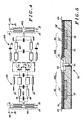
- An amplifier0 ⁇ 40 ( Figure 4, in which baluns are shown in schematic representation) comprises two transistors 41,41′ arranged in a push-pull configuration.
- the actual circuit suitable in a given application being within the competence of those skilled in the art.
- An input signal for amplification may be applied at single-ended input 45.
- a balun 48 in accordance with the present invention provides complementary balanced signals on lines 49,49′ to drive the push-pull pair 41,41′ form the printed matching network 405, which in turn provides a balanced amplified output on lines 400,400′ via a second matching network 406 including microstrip lines, such as line 407 to be converted to a single-ended final output at 401 by balun 402.
- the baluns 48 and 402 have capacitors 403,404 connected across their respective balanced ports to compensate for leakages in wide-band applications.
- 50 ( Figure 5) is mounted on a printed circuit board 51 which may be made of teflon/glass material as suitable for r.f. applications.
- Baluns 48 and 49 have conductors 20′,22′ and 20 ⁇ ,22 ⁇ respectively present on respective sides of the board 51.
- the conductors are surrounded by ground plane 30′.
- Power transistors (41,41′) in a single package 55 has its metal mounting plate0 ⁇ 52 fixed to a metal heat-sink 53 by bolt 54 so that it is connected to ground.
- the base and collector transistor supplies may be connected via decoupled baluns of the type shown in Figure 3(c).
- Heatsink 53 is required to be massive in view of the high heat dissipation of transistor, which typically would be operating in class AB, or even class A both of which are relatively inefficient, hence heatsink 53 extends the length of board 51 to provide a compact structure as is required to keep a complete high power r.f. amplifier (consisting of many such amplifiers) of reasonable size. Cut outs 57,58 are provided in heatsink 53 to accommodate the underside conductors of baluns 48,49 respectively.
- balun 48 the balanced side conductors (22′ for balun 48, 22 ⁇ for balun 49) are each affected uniformly by any parasitism there may be due to the proximity of heatsink 53, that is both sides of the balanced output (balun 48) or balanced input (balun 49) are equally affected.
- baluns are printed flat as part of the amplifier printed circuit board. This is a departure from prior art printed balun arrangements where the balanced side is formed part above and part below the printed circuit board leading to unacceptably asymmetric parasitic effects.
Landscapes
- Engineering & Computer Science (AREA)
- Power Engineering (AREA)
- Microelectronics & Electronic Packaging (AREA)
- Amplifiers (AREA)
- Microwave Amplifiers (AREA)
- Coils Or Transformers For Communication (AREA)
Abstract
Description
- The present invention relates to baluns, that is transformers capable of matching a single-ended output to a balanced input and vice versa.
- As an example of the application of a balun consider a high power transistor amplifier. Where output power requirements exceed that which can be delivered by a single transistor, a plurality of transistors may be coupled to share the power demand. In the base station of a cellular radio network, for example, operating in the high frequency region of 900 MHz, an output power requirement at the antenna feed of 1 kwatt would be typical, delivered by ten 100 watt amplifier modules. Presently the upper limit power capability of radio-frequency (r.f.) power transistors is in the region of 60 watt, hence to provide such a 100 watt module coupled transistors must be used.
- A convenient and useful method of coupling two transistors is the technique known in the art as "push-pull". Here the drive is shared between a transistor driving current through the load in one direction and a second transistor driving current through the load in the opposite direction. The arrangement is advantageous in terms of impedance matching, presenting a higher output impedance than the very low impedance of a single transistor or the yet lower impedance of parallel transistors, the higher output impedance being closer to the typical target impedance of 50, but unfortunately is inherently a balanced system, that is it produces an output signal which is symmetrical with respect to the common ground potential of the coupled transistors, whereas typically a single-ended (that is ground referenced) output signal is required. A solution to this problem is to provide a transformer between the output of the push-pull pair and the load. By virtue of its isolating properties, a transformer is able to couple the balanced output to the single-ended load. Such a transformer is that referred to in the art as a balun.
- In the case of push-pull arrangement, a similar problem exists in providing the complementary balanced drive signals required by the push-pull pair from a single-ended input signal to be amplifier, here a balun may be used to covert such an unbalanced input to the balanced drive signals.
- Many forms of balun, including transmission line forms, are known in the art. Examples have been described by C.L. Ruthroff in his paper "Some Broad-Band Transformers" (Proceedings of the Institute of Radio Engineers, 1959), pages 1337-1342".
- In high frequency r.f. amplifier applications a coaxial cable transmission line balun is typically used, for example a quarter wavelength length of cable having its outer conductor grounded at the single-ended side. An applied single-ended input will then generate a balanced output between the cable conductors at the remote end of the cable; equally a balanced signal applied to the non-grounded side will produce a single-ended output. The incorporation of such baluns in r.f. push-pull amplifier circuits will be known to those skilled in the art.
- Although providing good performance, there are a number of drawbacks associated with coaxial cable baluns. The baluns are made by cutting coaxial cable to length and at high frequency even small inaccuracies in length affect performance, also the nature of the cable component is not susceptible to mechanised placement and soldering. Hence the manufacturing tolerances associated with manual assembly create performance variations between one amplifier and another. In an attempt to overcome this problem baluns of printed form, which give good repeatability, have been tried. Printed circuit forms of baluns are known (see for example U.S. patent 4,193,048 issued to Nyhus). Unfortunately, a conventional construction printed flat on a circuit board cannot be used in high power applications due to the proximity of the large metal heatsinks associated with the amplifying transistors. Inevitably, one side of the circuit board is closer to the metal than the other causing an unacceptable imbalance in parasitic capacitances applied to the balun. To date, only simple printed forms have been used on separate boards mounted normal to the amplifier circuit board to give parasitic symmetry. Such boards are mechanically vulnerable and although repeatable in themselves, cannot be automatically assembled.
- The present invention, by contrast, provides a balun construction, useful in high power applications which may be printed flat.
- According to the present invention a balun providing a single-ended signal port and a balanced signal port, the balun includes:-
a plurality of serially connected first connector elements extending between said single-ended signal port and ground,
and a plurality of second conductor elements transformingly coupled to the first conductor elements and electrically isolated therefrom,
said second conductor elements extending in electrical symmetry from ground to said balanced port. - Preferably the conductor elements take the form of a contiguous merged conductor, which may be of similar form, such as, for example of closed loop form. Advantageously, the second conductor elements extend from a common ground. The conductors may be realised in printed circuit form.
- In a preferred form of the present invention suitable for wide band applications, a leakage compensation capacitor is connected at the balanced output port and conductor elements may be surrounded by a grounded conductor.
- A balun in accordance with the present invention may be used in an amplifier, such as a high power r.f. amplifier including a push-pull stage.
- In order that features and advantages of the present invention may be further appreciated embodiments will now be described, by way of example only, with reference to the accompanying diagrammatic drawings, of which:-
- Figure 1 represents a balun in accordance with the present invention;
- Figure 2 represents a form of the balun of Figure0̸1;
- Figure 3(a) represents a view of a printed circuit form of balun in accordance with the present invention from one side of a printed circuit board;
- Figure 3(b) represents opposite side;
- Figure 3(c) represents the decoupled version of Figure 3(a);
- Figure 4 represents a push-pull r.f. power amplifier including baluns in accordance with the present invention; and
- Figure 5 is a sectional view of the amplifier of Figure 4 constructed on a printed circuit board.
- A balun 10 (Figure 1) provides a single-
ended signal port 11 and abalanced signal port 12.Conductor elements ended port 11 to aground 16.Conductor elements balanced port 12 togrounds Conductor elements conductor elements balanced signal port 12 by virtue of transformer coupling (indicated diagrammatically at 100) between the first conductor pair (14,15) acting as a primary and the second conductor pair (16,17) acting as a secondary. For example, a signal due to a single-ended generator 101 may drive abalanced load 102 of value Zo. Alternatively, a balanced signal applied to thebalanced port 12 yields a single-ended output signal atport 11. In thisarrangement conductors conductors - In a preferred form of the present invention,
conductors grounds common point 21 which is a cold point, and which can be decoupled by acapacitor 22 to connect a power supply feed 23 (Figure 3(c)), so thatconductors single conductor 22. Otherwise similar parts bear the same reference numerals as in Figure 1. - It will be appreciated that this form of the present invention lends itself to fabrication on a printed circuit board construction,
conductors conductor 20 on one side of the printed circuit,conductor 22 on the other side andport connections ground plane 30. Proximity of the ground plane establishes this as the principle source of parasitic capacitances coupled to the transformer, hence reducing the effect of other stray capacitances which may be present. The ground plane may be omitted in the upper surface of the board, if desired. - A number of advantages of this printed form of the present invention will now be apparent to those skilled in the art. The balun is printed flat on the printed circuit board, which may be the same printed circuit board as carries an amplifier, for example, and so is repeatable with printed circuit board precision. No assembly is required and there is no component or assembly tolerance to affect circuit performance.
- The embodiments of the balun described thus far are suitable for use in a high frequency r.f. power amplifier circuit utilising transistors in push-pull. An amplifier0̸40 (Figure 4, in which baluns are shown in schematic representation) comprises two transistors 41,41′ arranged in a push-pull configuration. The actual circuit suitable in a given application being within the competence of those skilled in the art. An input signal for amplification may be applied at single-ended
input 45. Abalun 48 in accordance with the present invention provides complementary balanced signals onlines matching network 405, which in turn provides a balanced amplified output on lines 400,400′ via asecond matching network 406 including microstrip lines, such asline 407 to be converted to a single-ended final output at 401 bybalun 402. Thebaluns - In a constructed form of the push-pull amplifier of Figure 4, 50 (Figure 5) is mounted on a printed
circuit board 51 which may be made of teflon/glass material as suitable for r.f. applications.Baluns conductors 20′,22′ and 20˝,22˝ respectively present on respective sides of theboard 51. The conductors are surrounded byground plane 30′. Power transistors (41,41′) in asingle package 55, has its metal mounting plate0̸52 fixed to a metal heat-sink 53 bybolt 54 so that it is connected to ground. The base and collector transistor supplies may be connected via decoupled baluns of the type shown in Figure 3(c).Heatsink 53 is required to be massive in view of the high heat dissipation of transistor, which typically would be operating in class AB, or even class A both of which are relatively inefficient, hence heatsink 53 extends the length ofboard 51 to provide a compact structure as is required to keep a complete high power r.f. amplifier (consisting of many such amplifiers) of reasonable size. Cutouts heatsink 53 to accommodate the underside conductors ofbaluns - It will be appreciated that the balanced side conductors (22′ for
balun heatsink 53, that is both sides of the balanced output (balun 48) or balanced input (balun 49) are equally affected. - This is the important result which allows the baluns to be printed flat as part of the amplifier printed circuit board. This is a departure from prior art printed balun arrangements where the balanced side is formed part above and part below the printed circuit board leading to unacceptably asymmetric parasitic effects.
- The foregoing embodiments of the present invention have been described with reference to printed circuit board construction, being a suitable way of providing conductor elements electrically isolated by a dielectric carrier. It will be appreciated, nonetheless, that the present invention is applicable to all constructions providing electrically isolated conductors.
Claims (10)
a plurality of serially connected first connector elements extending between said single-ended signal port and ground,
and a plurality of second conductor elements transformingly coupled to the first conductor elements and electrically isolated therefrom,
said second conductor elements extending in electrical symmetry from ground to said balanced port.
Applications Claiming Priority (2)
| Application Number | Priority Date | Filing Date | Title |
|---|---|---|---|
| FR8912196A FR2652197B1 (en) | 1989-09-18 | 1989-09-18 | IMPROVED SYMMETRIC-DISSYMMETRIC TRANSFORMERS. |
| FR8912196 | 1989-09-18 |
Publications (2)
| Publication Number | Publication Date |
|---|---|
| EP0418538A1 true EP0418538A1 (en) | 1991-03-27 |
| EP0418538B1 EP0418538B1 (en) | 1995-03-15 |
Family
ID=9385588
Family Applications (1)
| Application Number | Title | Priority Date | Filing Date |
|---|---|---|---|
| EP90115279A Expired - Lifetime EP0418538B1 (en) | 1989-09-18 | 1990-08-09 | Improvements in or relating to balun transformers |
Country Status (8)
| Country | Link |
|---|---|
| US (1) | US5061910A (en) |
| EP (1) | EP0418538B1 (en) |
| JP (1) | JPH0828607B2 (en) |
| KR (1) | KR940000846B1 (en) |
| CA (1) | CA2024142C (en) |
| DE (1) | DE69017809T2 (en) |
| FR (1) | FR2652197B1 (en) |
| HK (1) | HK69497A (en) |
Cited By (7)
| Publication number | Priority date | Publication date | Assignee | Title |
|---|---|---|---|---|
| US5430895A (en) * | 1991-10-23 | 1995-07-04 | Nokia Mobile Phones, Ltd. | Transformer circuit having microstrips disposed on a multilayer printed circuit board |
| WO2003036716A1 (en) * | 2001-10-22 | 2003-05-01 | Infineon Technolgies Ag | Multi-stage, high frequency, high power signal amplifier |
| DE102004022185A1 (en) * | 2004-05-05 | 2005-12-01 | Rohde & Schwarz Gmbh & Co. Kg | Broadband balun transformer |
| WO2012047533A1 (en) * | 2010-10-06 | 2012-04-12 | Coherent, Inc. | Impedance -matching circuits for multi - output power supplies driving c02 gas -discharge lasers |
| US8354893B2 (en) | 2010-05-24 | 2013-01-15 | Coherent, Inc. | Impedance-matching transformers for RF driven CO2 gas discharge lasers |
| CN103339825A (en) * | 2011-05-11 | 2013-10-02 | 松下电器产业株式会社 | Electromagnetic Resonance Coupler |
| WO2020058361A1 (en) | 2018-09-18 | 2020-03-26 | Prodrive Technologies B.V. | Rf power amplifier with balun transformer |
Families Citing this family (59)
| Publication number | Priority date | Publication date | Assignee | Title |
|---|---|---|---|---|
| US5304959A (en) * | 1992-10-16 | 1994-04-19 | Spectrian, Inc. | Planar microstrip balun |
| JP2773617B2 (en) * | 1993-12-17 | 1998-07-09 | 株式会社村田製作所 | Balun Trance |
| US5451914A (en) * | 1994-07-05 | 1995-09-19 | Motorola, Inc. | Multi-layer radio frequency transformer |
| US5534830A (en) * | 1995-01-03 | 1996-07-09 | R F Prime Corporation | Thick film balanced line structure, and microwave baluns, resonators, mixers, splitters, and filters constructed therefrom |
| US5745017A (en) * | 1995-01-03 | 1998-04-28 | Rf Prime Corporation | Thick film construct for quadrature translation of RF signals |
| US5774801A (en) * | 1995-08-23 | 1998-06-30 | Ericsson Inc. | High dynamic range mixer having low conversion loss, low local oscillator input power, and high dynamic range and a method for designing the same |
| DE59610138D1 (en) | 1995-11-22 | 2003-03-20 | Schleifring Und Appbau Gmbh | DEVICE FOR TRANSMITTING SIGNALS BETWEEN MOVABLE PARTS |
| US5819169A (en) * | 1996-05-10 | 1998-10-06 | Northrop Grumman Corporation | High performance mixer structures for monolithic microwave integrated circuits |
| US5697088A (en) * | 1996-08-05 | 1997-12-09 | Motorola, Inc. | Balun transformer |
| JPH10116732A (en) * | 1996-10-09 | 1998-05-06 | Nec Corp | Transmission line transformer and amplifier unit employing it |
| US5808518A (en) * | 1996-10-29 | 1998-09-15 | Northrop Grumman Corporation | Printed guanella 1:4 balun |
| US5777527A (en) * | 1996-10-31 | 1998-07-07 | Motorola, Inc. | Method and apparatus for coupling a differential signal to an unbalanced port |
| FI103614B1 (en) * | 1997-03-20 | 1999-07-30 | Nokia Mobile Phones Ltd | Phasing and balancing means |
| US5886589A (en) * | 1997-05-30 | 1999-03-23 | Analog Devices, Incorporated | Balanced to unbalanced transmission line transformers |
| US6201439B1 (en) | 1997-09-17 | 2001-03-13 | Matsushita Electric Industrial Co., Ltd. | Power splitter/ combiner circuit, high power amplifier and balun circuit |
| US6294965B1 (en) | 1999-03-11 | 2001-09-25 | Anaren Microwave, Inc. | Stripline balun |
| SE0004794L (en) | 2000-12-22 | 2002-06-23 | Ericsson Telefon Ab L M | A multilayer symmetry transformer structure |
| DE10105696A1 (en) * | 2001-02-08 | 2002-08-14 | Rohde & Schwarz | Balun |
| US6531943B2 (en) * | 2001-04-20 | 2003-03-11 | Chung Shan Institute Of Science And Technology | Balun-transformer |
| US6529090B2 (en) | 2001-05-15 | 2003-03-04 | Lockheed Martin Corporation | Two-sided printed circuit anti-symmetric balun |
| US6483415B1 (en) * | 2001-05-21 | 2002-11-19 | Industrial Technology Research Institute | Multi-layer LC resonance balun |
| US6424227B1 (en) | 2001-05-23 | 2002-07-23 | National Scientific Corporation | Monolithic balanced RF power amplifier |
| US6577219B2 (en) | 2001-06-29 | 2003-06-10 | Koninklijke Philips Electronics N.V. | Multiple-interleaved integrated circuit transformer |
| US6927647B2 (en) * | 2002-06-11 | 2005-08-09 | Ernesto G. Starri | Two channels, high speed, RF switch |
| US6819200B2 (en) * | 2002-07-26 | 2004-11-16 | Freescale Semiconductor, Inc. | Broadband balun and impedance transformer for push-pull amplifiers |
| US6683510B1 (en) | 2002-08-08 | 2004-01-27 | Northrop Grumman Corporation | Ultra-wideband planar coupled spiral balun |
| JP2004304615A (en) * | 2003-03-31 | 2004-10-28 | Tdk Corp | High frequency composite part |
| US20070229368A1 (en) * | 2004-08-27 | 2007-10-04 | Hiroshi Hata | Planar coupler and integrated antenna system |
| WO2006022046A1 (en) * | 2004-08-27 | 2006-03-02 | Higuchi, Toshiaki | High frequency coupler, high frequency tansmitter and antenna |
| US7495525B2 (en) * | 2005-08-23 | 2009-02-24 | Synergy Microwave Corporation | Multilayer planar balun transformer, mixers and amplifiers |
| JP4730233B2 (en) * | 2006-07-11 | 2011-07-20 | 旭硝子株式会社 | Transmission line converter |
| US7724484B2 (en) * | 2006-12-29 | 2010-05-25 | Cobham Defense Electronic Systems Corporation | Ultra broadband 10-W CW integrated limiter |
| JP4645976B2 (en) * | 2007-02-28 | 2011-03-09 | 三菱電機株式会社 | Balun |
| US7633353B2 (en) * | 2007-10-22 | 2009-12-15 | Advantest Corporation | Balun circuit and frequency converting apparatus |
| US20100060541A1 (en) * | 2008-09-08 | 2010-03-11 | Smartant Telecom Co., Ltd. | Antenna |
| US7880557B2 (en) * | 2009-03-12 | 2011-02-01 | Hittite Microwave Corporation | Hybrid marchand/back-wave balun and double balanced mixer using same |
| EP2471078A1 (en) * | 2009-08-27 | 2012-07-04 | Telefonaktiebolaget L M Ericsson (PUBL) | An improved transformer |
| ES2711352T3 (en) | 2010-06-11 | 2019-05-03 | Ricoh Co Ltd | Information storage device, removable device, developer container and image forming device |
| US8498604B2 (en) | 2010-06-22 | 2013-07-30 | Hittite Microwave Corporation | Double balanced mixer |
| SG11201400409XA (en) * | 2011-09-07 | 2014-04-28 | Solace Power Inc | Wireless electric field power transmission system and method |
| KR101214722B1 (en) * | 2011-11-22 | 2012-12-21 | 삼성전기주식회사 | Transformer and method for manufacturing thereof |
| WO2013128795A1 (en) | 2012-02-29 | 2013-09-06 | パナソニック株式会社 | Electromagnetic resonance coupler |
| RU2014139849A (en) | 2012-03-02 | 2016-04-27 | Конинклейке Филипс Н.В. | DEVICE AND METHOD FOR AMPLIFIING RADIO FREQUENCY SIGNAL |
| DE102012106135A1 (en) | 2012-07-09 | 2014-05-22 | Cryoelectra Gmbh | Baluns for use in amplifier unit of high frequency amplifier of e.g. base station of radio system, have layered structure provided with underside that is connected to temperature heat sink element directly or indirectly over metallic layer |
| ITMI20121238A1 (en) * | 2012-07-17 | 2014-01-18 | St Microelectronics Srl | BALUN PLANAR TRANSFORMER DEVICE |
| US9300022B2 (en) | 2013-04-05 | 2016-03-29 | Scientific Components Corporation | Vaisman baluns and microwave devices employing the same |
| JP6318548B2 (en) | 2013-10-29 | 2018-05-09 | 富士通株式会社 | Amplifier circuit |
| EP2899803B1 (en) * | 2014-01-24 | 2020-06-24 | Ampleon Netherlands B.V. | Circuit comprising balun and impedance transforming elements |
| CA2953621A1 (en) | 2014-06-26 | 2015-12-30 | Solace Power Inc. | Wireless electric field power transmission system, transmitter and receiver therefor and method of wirelessly transferring power |
| WO2016033697A1 (en) | 2014-09-05 | 2016-03-10 | Solace Power Inc. | Wireless electric field power transfer system, method, transmitter and receiver therefor |
| WO2016099314A1 (en) | 2014-12-15 | 2016-06-23 | Siemens Research Center Limited Liability Company | A balun transformer with a cooling mechanism |
| EP3218957A1 (en) * | 2014-12-15 | 2017-09-20 | Siemens Aktiengesellschaft | A fluid-cooled balun transformer |
| TWM499657U (en) * | 2015-01-26 | 2015-04-21 | Trans Electric Co Ltd | Balun |
| US9692387B2 (en) * | 2015-07-24 | 2017-06-27 | Nxp Usa, Inc. | Balun transformer |
| CN112259341A (en) * | 2015-10-26 | 2021-01-22 | 鲲腾科技有限公司 | Magnetic structure with self-closing magnetic circuit |
| JP6497564B2 (en) * | 2015-12-17 | 2019-04-10 | 株式会社Wave Technology | Balun transformer and electronic equipment using the same |
| DE102017208917A1 (en) | 2017-05-26 | 2018-11-29 | TRUMPF Hüttinger GmbH + Co. KG | High-frequency amplifier arrangement and method for designing a high-frequency amplifier arrangement |
| EP3605842A1 (en) | 2018-08-02 | 2020-02-05 | TRUMPF Huettinger Sp. Z o. o. | Balun and amplifier including the balun |
| KR102706225B1 (en) | 2021-12-10 | 2024-09-19 | 충남대학교산학협력단 | Circuit for generating differential signal |
Citations (3)
| Publication number | Priority date | Publication date | Assignee | Title |
|---|---|---|---|---|
| GB1233894A (en) * | 1967-06-19 | 1971-06-03 | ||
| GB2084809A (en) * | 1980-10-01 | 1982-04-15 | Communications Patents Ltd | Printed circuit transformers |
| WO1987007074A1 (en) * | 1986-05-08 | 1987-11-19 | American Telephone & Telegraph Company | Transformer structure |
Family Cites Families (5)
| Publication number | Priority date | Publication date | Assignee | Title |
|---|---|---|---|---|
| US3656071A (en) * | 1970-06-25 | 1972-04-11 | Rca Corp | Wide band balun |
| US3991390A (en) * | 1975-07-31 | 1976-11-09 | Motorola, Inc. | Series connected stripline balun |
| JPS5857001A (en) * | 1981-09-30 | 1983-04-05 | Hitachi Ltd | Scroll for fluid machinery and its manufacturing method |
| JPS63246001A (en) * | 1987-04-01 | 1988-10-13 | Tokyo Keiki Co Ltd | Push-pull transformer for high frequency application |
| US4980654A (en) * | 1990-04-06 | 1990-12-25 | Tektronix, Inc. | Transmission line transformer |
-
1989
- 1989-09-18 FR FR8912196A patent/FR2652197B1/en not_active Expired - Lifetime
-
1990
- 1990-08-09 DE DE69017809T patent/DE69017809T2/en not_active Expired - Fee Related
- 1990-08-09 EP EP90115279A patent/EP0418538B1/en not_active Expired - Lifetime
- 1990-08-27 US US07/572,737 patent/US5061910A/en not_active Expired - Fee Related
- 1990-08-28 CA CA002024142A patent/CA2024142C/en not_active Expired - Fee Related
- 1990-09-11 JP JP2241029A patent/JPH0828607B2/en not_active Expired - Fee Related
- 1990-09-13 KR KR1019900014429A patent/KR940000846B1/en not_active Expired - Fee Related
-
1997
- 1997-05-22 HK HK69497A patent/HK69497A/en not_active IP Right Cessation
Patent Citations (3)
| Publication number | Priority date | Publication date | Assignee | Title |
|---|---|---|---|---|
| GB1233894A (en) * | 1967-06-19 | 1971-06-03 | ||
| GB2084809A (en) * | 1980-10-01 | 1982-04-15 | Communications Patents Ltd | Printed circuit transformers |
| WO1987007074A1 (en) * | 1986-05-08 | 1987-11-19 | American Telephone & Telegraph Company | Transformer structure |
Non-Patent Citations (1)
| Title |
|---|
| IEEE TRANSACTIONS ON MAGNETICS. vol. 21, no. 2, March 1985, NEW YORK US pages 652 - 653; M.GERSHENSON: "Integrated squid linear amplifier design and simulation" * |
Cited By (11)
| Publication number | Priority date | Publication date | Assignee | Title |
|---|---|---|---|---|
| US5430895A (en) * | 1991-10-23 | 1995-07-04 | Nokia Mobile Phones, Ltd. | Transformer circuit having microstrips disposed on a multilayer printed circuit board |
| WO2003036716A1 (en) * | 2001-10-22 | 2003-05-01 | Infineon Technolgies Ag | Multi-stage, high frequency, high power signal amplifier |
| DE102004022185A1 (en) * | 2004-05-05 | 2005-12-01 | Rohde & Schwarz Gmbh & Co. Kg | Broadband balun transformer |
| WO2005109975A3 (en) * | 2004-05-05 | 2006-04-06 | Rohde & Schwarz | Broadband balance-to-unbalance transformer |
| US7656247B2 (en) | 2004-05-05 | 2010-02-02 | Rohde & Schwarz Gmbh & Co., Kg | Broadband balancing transformer |
| US8354893B2 (en) | 2010-05-24 | 2013-01-15 | Coherent, Inc. | Impedance-matching transformers for RF driven CO2 gas discharge lasers |
| WO2012047533A1 (en) * | 2010-10-06 | 2012-04-12 | Coherent, Inc. | Impedance -matching circuits for multi - output power supplies driving c02 gas -discharge lasers |
| US8648665B2 (en) | 2010-10-06 | 2014-02-11 | Coherent, Inc. | Impedance-matching circuits for multi-output power supplies driving CO2 gas-discharge lasers |
| CN103339825A (en) * | 2011-05-11 | 2013-10-02 | 松下电器产业株式会社 | Electromagnetic Resonance Coupler |
| CN103339825B (en) * | 2011-05-11 | 2015-12-23 | 松下电器产业株式会社 | Electromagnetic resonance coupler |
| WO2020058361A1 (en) | 2018-09-18 | 2020-03-26 | Prodrive Technologies B.V. | Rf power amplifier with balun transformer |
Also Published As
| Publication number | Publication date |
|---|---|
| EP0418538B1 (en) | 1995-03-15 |
| FR2652197A1 (en) | 1991-03-22 |
| JPH0828607B2 (en) | 1996-03-21 |
| CA2024142C (en) | 1994-11-08 |
| CA2024142A1 (en) | 1991-03-19 |
| DE69017809T2 (en) | 1995-11-02 |
| KR910007174A (en) | 1991-04-30 |
| JPH03237801A (en) | 1991-10-23 |
| FR2652197B1 (en) | 1992-09-18 |
| DE69017809D1 (en) | 1995-04-20 |
| KR940000846B1 (en) | 1994-02-02 |
| US5061910A (en) | 1991-10-29 |
| HK69497A (en) | 1997-05-30 |
Similar Documents
| Publication | Publication Date | Title |
|---|---|---|
| US5061910A (en) | Balun transformers | |
| US5973567A (en) | Tunable impedance matching network for a mic power amplifier module | |
| US5736908A (en) | Waveguide-based spatial power combining array and method for using the same | |
| US6771222B1 (en) | Phase-array antenna diplexing | |
| EP1331689B1 (en) | Power splitter/combiner circuit | |
| US7084715B2 (en) | Coupling device | |
| CA2236993C (en) | Hybrid circuit construction of push-pull power amplifier | |
| US4641106A (en) | Radial power amplifier | |
| WO2007106443A2 (en) | Monolithic integrated transceiver | |
| US6542035B2 (en) | Modular high power solid state amplifier | |
| EP0189597B1 (en) | Monolithic series feedback low noise fet amplifiers | |
| WO1997017738A1 (en) | Slotline-to-coplanar waveguide transition | |
| US6265937B1 (en) | Push-pull amplifier with dual coplanar transmission line | |
| US5008633A (en) | Cross-fed FET power-chip | |
| Barnes et al. | A compact 6 to 18 GHz power amplifier module with 10 W output power | |
| US4727351A (en) | High power RF resistor | |
| CA2237018C (en) | Method for making a circuit structure having a flip-mounted matrix of devices | |
| CA2236999C (en) | Circuit structure having a flip-mounted matrix of devices | |
| Meier et al. | Integrated X-band sweeping superheterodyne receiver | |
| CA2236983C (en) | Slotline-to-coplanar waveguide transition | |
| Bettner et al. | Low Cost MMIC Insertion Using Thick Film Processing | |
| JPH03266501A (en) | Microwave circuit device |
Legal Events
| Date | Code | Title | Description |
|---|---|---|---|
| PUAI | Public reference made under article 153(3) epc to a published international application that has entered the european phase |
Free format text: ORIGINAL CODE: 0009012 |
|
| AK | Designated contracting states |
Kind code of ref document: A1 Designated state(s): DE GB IT NL SE |
|
| 17P | Request for examination filed |
Effective date: 19910905 |
|
| 17Q | First examination report despatched |
Effective date: 19920622 |
|
| RAP1 | Party data changed (applicant data changed or rights of an application transferred) |
Owner name: MOTOROLA SEMICONDUCTEURS S.A. |
|
| ITF | It: translation for a ep patent filed | ||
| GRAA | (expected) grant |
Free format text: ORIGINAL CODE: 0009210 |
|
| AK | Designated contracting states |
Kind code of ref document: B1 Designated state(s): DE GB IT NL SE |
|
| REF | Corresponds to: |
Ref document number: 69017809 Country of ref document: DE Date of ref document: 19950420 |
|
| PLBE | No opposition filed within time limit |
Free format text: ORIGINAL CODE: 0009261 |
|
| STAA | Information on the status of an ep patent application or granted ep patent |
Free format text: STATUS: NO OPPOSITION FILED WITHIN TIME LIMIT |
|
| 26N | No opposition filed | ||
| PGFP | Annual fee paid to national office [announced via postgrant information from national office to epo] |
Ref country code: NL Payment date: 19990630 Year of fee payment: 10 |
|
| PGFP | Annual fee paid to national office [announced via postgrant information from national office to epo] |
Ref country code: SE Payment date: 19990802 Year of fee payment: 10 |
|
| PG25 | Lapsed in a contracting state [announced via postgrant information from national office to epo] |
Ref country code: SE Free format text: LAPSE BECAUSE OF NON-PAYMENT OF DUE FEES Effective date: 20000810 |
|
| PG25 | Lapsed in a contracting state [announced via postgrant information from national office to epo] |
Ref country code: NL Free format text: LAPSE BECAUSE OF NON-PAYMENT OF DUE FEES Effective date: 20010301 |
|
| EUG | Se: european patent has lapsed |
Ref document number: 90115279.3 |
|
| NLV4 | Nl: lapsed or anulled due to non-payment of the annual fee |
Effective date: 20010301 |
|
| REG | Reference to a national code |
Ref country code: GB Ref legal event code: IF02 |
|
| PG25 | Lapsed in a contracting state [announced via postgrant information from national office to epo] |
Ref country code: IT Free format text: LAPSE BECAUSE OF NON-PAYMENT OF DUE FEES;WARNING: LAPSES OF ITALIAN PATENTS WITH EFFECTIVE DATE BEFORE 2007 MAY HAVE OCCURRED AT ANY TIME BEFORE 2007. THE CORRECT EFFECTIVE DATE MAY BE DIFFERENT FROM THE ONE RECORDED. Effective date: 20050809 |
|
| PGFP | Annual fee paid to national office [announced via postgrant information from national office to epo] |
Ref country code: GB Payment date: 20060706 Year of fee payment: 17 |
|
| PGFP | Annual fee paid to national office [announced via postgrant information from national office to epo] |
Ref country code: DE Payment date: 20060831 Year of fee payment: 17 |
|
| GBPC | Gb: european patent ceased through non-payment of renewal fee |
Effective date: 20070809 |
|
| PG25 | Lapsed in a contracting state [announced via postgrant information from national office to epo] |
Ref country code: DE Free format text: LAPSE BECAUSE OF NON-PAYMENT OF DUE FEES Effective date: 20080301 |
|
| PG25 | Lapsed in a contracting state [announced via postgrant information from national office to epo] |
Ref country code: GB Free format text: LAPSE BECAUSE OF NON-PAYMENT OF DUE FEES Effective date: 20070809 |