EP0421423A2 - Method of controlling filter time constant and filter circuit having the time constant control function based on the method - Google Patents
Method of controlling filter time constant and filter circuit having the time constant control function based on the method Download PDFInfo
- Publication number
- EP0421423A2 EP0421423A2 EP90119053A EP90119053A EP0421423A2 EP 0421423 A2 EP0421423 A2 EP 0421423A2 EP 90119053 A EP90119053 A EP 90119053A EP 90119053 A EP90119053 A EP 90119053A EP 0421423 A2 EP0421423 A2 EP 0421423A2
- Authority
- EP
- European Patent Office
- Prior art keywords
- filter
- signal
- time constant
- control
- controller
- Prior art date
- Legal status (The legal status is an assumption and is not a legal conclusion. Google has not performed a legal analysis and makes no representation as to the accuracy of the status listed.)
- Granted
Links
Images


Classifications
-
- H—ELECTRICITY
- H03—ELECTRONIC CIRCUITRY
- H03H—IMPEDANCE NETWORKS, e.g. RESONANT CIRCUITS; RESONATORS
- H03H11/00—Networks using active elements
- H03H11/02—Multiple-port networks
- H03H11/04—Frequency selective two-port networks
- H03H11/12—Frequency selective two-port networks using amplifiers with feedback
- H03H11/1291—Current or voltage controlled filters
Definitions
- the present invention relates to a method of controlling the time constant of a filter and a filter circuit having the time constant control function based on the method, and more particularly to a time cosntant control method suitable for a filter of a receiving unit of a paging radio receiver which is required to be reduced in voltage, power and size.
- a filter for filtering an input signal hereinafter referred to as a main filter
- a control circuit for controlling the time constant of the main filter and an artificial filter having the same construction as that of the main filter, whereby a standard pulse signal having a predetermined frequency is applied or inputted to the artificial filter so that the aritifical filter may deliver an output signal the level of which is compared with a predetermined reference level.
- a voltage or current complying with an error between the output and reference levels is fed back to the artificial filter and supplied to the main filter, in a polarity which cancels the error.
- a filter time constant control method comprises the steps of inputting a standard pulse signal having a predetermined frequency and a predetermined signal level to a filter in advance of each time that filtering of an input signal is effected at a predetermined timing, comparing an output signal level from the filter with a predetermined reference level, and adjusting the time constant of the filter in accordance with the comparison results.
- a radio receiving method applicable to a radio receiver in which circuits within the radio receiver are operated intermittently at a predetermined period, and a received signal is filtered during each operation interval and thereafter demodulated and delivered comprises the steps of controlling the time constant of a filter in the radio receiver during a first time zone within each operation interval, and filtering, demodulating and delivering the received signal during a second time zone following completion of the time constant control.
- the controller for controlling the time constant of the filter applies the standard pulse signal to the filter during a predetermined interval (for example, 3 msec) beginning with a predetermined timing following rise of the BS signal (for example, 10 msec after the rise), and a level of an output signal from the filter is compared with a predetermined reference level, whereby the filter time constant control is effected and after completion of each time constant control, the received signal is switched to the filter, demodulated by the demodulating circuit and delivered (in the form of, for example, sound or display).
- a predetermined interval for example, 3 msec
- a predetermined timing following rise of the BS signal for example, 10 msec after the rise
- the baseband circuit 7 responds to the contents of a signal (control signal) received precedently from a transmitting station through the antenna to deliver the battery-saving signal (BS signal) at a predetermined period during a predetermined interval which starts at a certain timing. For example, when the transmitting station communicates with a plurality of receivers on time division base, a control signal transmitted from the transmitting station to each receiver contains information concerning time slots to be allotted to each receiver. Thus, the baseband circuit 7 delivers, at a start timing designated by the information, the BS signal at the predetermined period during the predetermined interval. A specified timing chart will be described later with reference to Figs. 2 and 3.
- the receiver controls the time constant of the filter, and demodulates and delivers the signal received from the transmitting station.
- the time constant of the filter is controlled in advance.
- the delivery of the BS signal is repeated at the predetermined period but in Fig. 2, only one period of the BS signal is illustrated.
- the start pulse clock signal generator 36 delivers the ST signal for determining the start of the control operation and the standard clock pulse signal (CL1 signal).
- a timing signal generator 33 receives these two pulse signals and delivers a clock pulse signal (CL2 signal) for determining the frequency of the standard clock signal PL and a clock pulse signal (CL3 signal) for causing a switch controller 32 to control the timing for switch control.
- the standard pulse signal generator 31 responds to the clock pulse CL2 to determine the frequency of the standard pulse signal PL and to the reference voltage V ref to determine the amplitude level of the standard pusle signal PL.
- the switch controller 32 delivers switch drive signals SD1, SD2 and SD3 and the aforementioned END signal. Timings for these signals are determined by the input clock CL3.
- the "H” or “L” state of the switch drive signals SD1, SD2 and SD3 (“H” for turn-on of switch and “L” for turn-off of switch) is sequentially determined in accordance with the "H” or "L” polarity of a decision output signal THO of a comparator 35.
- the switch controller 32 sets the SD3 to "H” in order to render the switches 313 and 323 "ON” and at the same time sets the control end pulse (END signal) to "H".
- END signal control end pulse
- the total filter capacitance Cc can be changed through the above capacitor control operation as shown at the bottom section in Fig. 3. At the end of the control operation, the value of Cc measures 15(pF) within the adjusting range of from 10 to 17(pF).
- the control switches 311 t 313 and 321 to 323 are set in such a manner that all the switches are rendered “ON” upon start and the switch drive pulses are rendered “L” sequentially beginning with the drive signal SD1.
- a method based on the inverted polarity may be employed wherein all the switches are rendered "OFF” upon start and the switch drive pulses are rendered "H” sequentially beginning with the SD1 signal.
- the filter time constant control system of the invention has been described as applied to the paging radio receiver which performs the receiving operation periodically.
- the filter time constant control system according to the invention may also be applied to an apparatus wherein a filter is comprised in the apparatus, the time constant of the filter is controlled for correction and thereafter the controlled and corrected filter is used for an intended signal processing.
- a radio, a television and a communication terminal may be enumerated as this type of apparatus.
- the connective relation between the filter 2 and time constant control circuit must be changed slightly.
- the filter output signal takes the form of an analog value
- the output signal of the filter 2 of Fig. 1 may be inputted directly to the level detector 34 and connected to output circuits handling the filter analog output signal as it is.
- a switch (SO) 92 has one end grounded and the other end connected to the input of an amplifier 22 provided for capacitors 220 to 223 of a filter 2.
- Waves ST, CL1, CL3 and END in Fig. 8 resemble those in Fig. 3 and their description will be omitted.
- the drive pulse SWP is to on/off control the switch (SO) 92 and in this example the switch is turned on with high level “H” of the drive pulse and turned off with low level “L” of the drive pulse.
- the output signal F OUT of the filter 2 stands for an input signal to the comparator 35. Simultaneously indicated on ordinate of a graph section indicating the F OUT waveform are a threshold voltage V TH of the comparator 35 and a DC voltage V B .
- the output signal, THO, of the comparator 35 is rendered high level "H” when the level of the input signal (F OUT ) 47 is higher than the threshold V TH but is rendered low level "L” when lower.
- the signals SD1, SD2 and SD3 start falling at the same timing or phase as that in the first embodiment (see Fig. 3) but start rising at earlier timings than those in the first embodiment (see Fig. 3). For these reasons, the waveform of the total capacitance Cc of the capacitors varies differently from that shown in Fig. 3 but the ultimate total capacitance Cc of the capacitors can also be converged to 15(pF).
- the filter capable of controlling the time constant can be reduced in its circuit area and power consumption.
- the fourth effect is such that the control time can be reduced by setting a ratio of capacitance (or resistance) among capacitors (resistors) used as time constant control elements to 4:2:1 to set up a ratio of 2:1 between sequential elements and by shifting the setting operation sequentially from the maximum bit to the minimum bit during the time constant controlling.
- the number of bits is 3 and the time constant control operation can be completed through three-times setting operations (about 3 msec).
Landscapes
- Networks Using Active Elements (AREA)
- Mobile Radio Communication Systems (AREA)
Abstract
Description
- The present invention relates to a method of controlling the time constant of a filter and a filter circuit having the time constant control function based on the method, and more particularly to a time cosntant control method suitable for a filter of a receiving unit of a paging radio receiver which is required to be reduced in voltage, power and size.
- In a conventional filter time constant control system, the op ration of filtering a received signal and the operation of controlling the time constant of a filter circuit for filtering are carried out in parallel.
- For example, there are provided a filter for filtering an input signal (hereinafter referred to as a main filter), a control circuit for controlling the time constant of the main filter, and an artificial filter having the same construction as that of the main filter, whereby a standard pulse signal having a predetermined frequency is applied or inputted to the artificial filter so that the aritifical filter may deliver an output signal the level of which is compared with a predetermined reference level. As a result of the comparison, a voltage or current complying with an error between the output and reference levels is fed back to the artificial filter and supplied to the main filter, in a polarity which cancels the error.
- In the above arrangement, when the relative accuracy (inclusive of control characteristics) between the main and artificial filters is designed to be high, the voltage or current fed back to the artificial filter can act on the main filter so as to cancel the error in the main filter.
- Incidentally, used as the time constant control element within the filter is, for example, "ON" resistance of variable capacitor diodes or D-MOS's which are controllable by voltage or "ON" resistance of diodes which are controllable by current; but capacitors and switches acting as control elements which are on/off controlled for connection of capacitors are not used. The reason for this is as follows. As described previously, in the conventional receiving system, filtering of the received signal and time constant control of the main filter are carried out in parallel and therefore, if the control element such as the capacitor is used as the time constant control element, then the switch will be turned on or off, causing a noise which interferes with the main filter.
- In another conventional system, an oscillator is constructed using time constant control elements whithin an artificial filter, a phase difference between an oscillation signal from the oscillator and a standard pulse signal having a predetermined frequency is detected, and a voltage complying with the phase difference is supplied to the artificial filter and a main filter. The voltage complying with the phase difference acts on the main filter as it acts on the artificial filter.
- The aforementioned conventional systems are disclosed in JP-A-60-214617 and "On-chip Automatic Tuning for a CMOS Continuous-Time Filter", by Mihai Banu et al., ISSCC85/FRIDAY, FEBRUARY 15, IEEE International Solid-State Circuits Conference.
- Today, it has been desired to make a filter in the form of an LSI with its size and power reduced and especially to realize a small-sized paging radio receiver of reduced power consumption by using the filter in the form of the LSI. However, a ceramic filter is widely used in the conventional paging radio receiver and the size reduction of the receiver is limited. Further, in realizing the filter portion with the LSI, the monolithic (main) filter using variable capacitor diodes as time constant control elements must be used in combination with the artificial filter of the same construction and control circuit which are adapted to control the main filter, as described previously. Accordingly, the total area of the filter circuit inclusive of the control circuit and artificial filter causes a bottleneck to size reduction. In addition, the time constant control is effected during the signal receiving operation and disadvantageously power consumption is increased correspondingly.
- Specifically, when the variable capacitor diode is used as the time constant control element of the filter, a control voltage of about 3V is required for controlling the capacitance of the filter by about ±25%. When the time constant control element is so designed that "ON" resistance of D-MOS transistors is controlled by a gate voltage, the filter must be a differential active filter in order to compensate harmonic distortion generated by non-linearity of the D-MOS transistors and the use of the differential active filter is unsuited for redution of the circuit area.
- An object of the invention is to provide a method of controlling the time constant of a filter having a small circuit area and operative at low power and low voltage, and a filter having the time constant control function.
- Another object of the invention is to provide a radio receiving method suitable for a radio receiver which uses the aforementioned filter so as to be reduced in circuit area and operative at low power and low voltage.
- To accomplish the first object, a filter time constant control method according to the invention comprises the steps of inputting a standard pulse signal having a predetermined frequency and a predetermined signal level to a filter in advance of each time that filtering of an input signal is effected at a predetermined timing, comparing an output signal level from the filter with a predetermined reference level, and adjusting the time constant of the filter in accordance with the comparison results.
- To accomplish the second object, according to the invention, a radio receiving method applicable to a radio receiver in which circuits within the radio receiver are operated intermittently at a predetermined period, and a received signal is filtered during each operation interval and thereafter demodulated and delivered, comprises the steps of controlling the time constant of a filter in the radio receiver during a first time zone within each operation interval, and filtering, demodulating and delivering the received signal during a second time zone following completion of the time constant control.
- Specifically, when the receiver is tuned to the transmitting station, a baseband circuit within the receiver responds to information allotted to time slots contained in a transmission signal to deliver a battery-saving signal (BS signal) at a predetermined period (21sec pursuant to the standard).
- Subsequently, the controller for controlling the time constant of the filter applies the standard pulse signal to the filter during a predetermined interval (for example, 3 msec) beginning with a predetermined timing following rise of the BS signal (for example, 10 msec after the rise), and a level of an output signal from the filter is compared with a predetermined reference level, whereby the filter time constant control is effected and after completion of each time constant control, the received signal is switched to the filter, demodulated by the demodulating circuit and delivered (in the form of, for example, sound or display).
- A plurality of capacitors are connected in parallel (or resistance elements are connected in series) within the filter, and the controller selects from them necessary capacitors (or resistance elements) by means of switches in order to control the filter time constant. A ratio of capacitance among the plurality of capacitors connected in parallel (in the case of resistance element, a ratio of resistance) is increased sequentially at the rate of two times, for example, in such a fashion as 1, 2, 4, 8, ....
- The filter output signal level is subjected to analog-digital (A/D) conversion by an analog-digital (A/D) converter and the controller compares the converted signal level with a predetermined reference level, threby performing the filter time constant control. Then, a reference voltage supplied to a standard pulse signal generator which generates the standard pulse signal inputted to the filter during the time constant control interval is used in common as a reference voltage used for A/D conversion by the A/D converter.
- In the filter time constant control method according to the invention, prior to performing filtering of an input signal received at a predetermined timing, the standard pulse signal having a predetermined frequency and a predetermined signal level is applied to the filter and the time constant of the filter is controlled in accordance with an output signal from the filter, thereby ensuring that the artifical filter and the like circuits needed conventionally can be dispensed with and the power consumption and circuit area can be reduced.
- The filter time constant control is carried out by turning on/off the switches to select necessary capacitors (or resistance elements) from the plurality of capacitors connected in parallel (or resistance elements connected in series) within the filter. Accordingly, the variable capacitor diode or differential active filter needed conventionally can be dispensed with, thus facilitating lowering of power supply voltage or size reduction of the filter per se.
- Further, by increasing the capacitance ratio between sequential or adjacent capacitors (or resistance ratio between sequential or adjacent resistors) among the plurality of capacitors connected in parallel (or resistors connected in series) at the rate of two times and performing sequential selection and setting of time constant bits beginning with the maximum bit and ending in the minimum bit, the setting can be completed through the same number of setting operations as the number of bits.
- Similarly, in the radio receiving method according to the invention, the time constant of the filter within the radio receiver is controlled during a predetermined interval following the start of each intermittent operation, and after completion of the filter time constant control, the received signal is demodulated during each predetermined interval, thereby ensuring that the artificial filter and the like circuits conventionally needed can be dispensed with and the power consumption and circuit area can be reduced.
- Further, by using the reference voltage supplied to the standard pulse signal generator which generates the standard pulse signal inputted to the filter in common as the reference voltage used for A/D conversion of the filter output signal by the A/D converter, the influence of errors contained in the standard pulse signal per se upon the gain change of the A/D converter can be cancelled out.
- The foregoing and other objects, advantages, manner of operation and novel features of the present invention will be understood from the following detailed description when read in connection with the accompanying drawings.
-
- Fig. 1 is a schematic block diagram of a paging radio receiver to which the filter time constant control method of the invention is applied;
- Fig. 2 is a time chart showing how the time constant control interval of filter and the demodulating interval of received signal are related to a battery-saving signal;
- Fig. 3 is a time chart showing clock signals and switch drive signals appearing during the filter time constant control interval;
- Fig. 4 is a circuit diagram of a filter in which the time constant is controlled by switching resistance;
- Fig. 5 is a time chart showing signals appearing during the time constant control interval of the filter shown in Fig. 4;
- Fig. 6 is a graph for explaining the frequency band of a standard pulse signal used for the filter time constant control;
- Fig. 7 is a schematic block diagram showing another embodiment of the paging radio receiver to which the filter time constant control method of the invention is applied; and
- Fig. 8 is a time chart showing clock signals and switch drive signals appearing during the filter time constant control interval in the Fig. 7 embodiment.
- An embodiment in which a filter time constant control system of the invention is applied to a paging radio receiver will now be described with reference to the accompanying drawings.
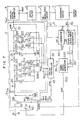
- Fig. 1 is a schematic diagram showing the paging radio receiver to which the invention is applied. In the figure,
reference numeral 1 designates an input switching circuit for selectively switching and receiving a signal received through an antenna (not shown) and a standard pulse signal for control of filter time constant, 2 a low-pass filter the time constant of which is variable, and 3 a control logic circuit for controlling the time constant of thefilter 2. Additionally, the receiver comprises an analog-digital (A/D)converter 4 for converting an analog signal delivered out of thefilter 2 into a digital signal, adigital filter 5, a demodulating circuit 6 for demodulating the digital signal, and abaseband circuit 7 for delivering a battery-saving signal (BS signal) to which the timing for intermittent operation of reception is referenced and also delivering an output signal to output circuits including a display, for exmaple. - The
baseband circuit 7 responds to the contents of a signal (control signal) received precedently from a transmitting station through the antenna to deliver the battery-saving signal (BS signal) at a predetermined period during a predetermined interval which starts at a certain timing. For example, when the transmitting station communicates with a plurality of receivers on time division base, a control signal transmitted from the transmitting station to each receiver contains information concerning time slots to be allotted to each receiver. Thus, thebaseband circuit 7 delivers, at a start timing designated by the information, the BS signal at the predetermined period during the predetermined interval. A specified timing chart will be described later with reference to Figs. 2 and 3. - For avoiding prolixity, output circuits (for example, liquid crystal display and the like) connected to the
baseband circuit 7 and a circuit for generation of a reference voltage Vref supplied to the A/D converter 4 and the like are not illustrated in the drawing. - During the interval for delivery of the BS signal, the receiver controls the time constant of the filter, and demodulates and delivers the signal received from the transmitting station. In the present embodiment, before filtering of an input signal is effected by means of the filter, the time constant of the filter is controlled in advance.
- The operation of demodulating a received signal after completion of control of the filter time constant will now be described.
- A received signal is inputted through a signal input terminal 8 (IN), passed through a switch 10 (SIN) in the
input switching circuit 1 and delivered to an input line (FIN) of thefilter circuit 2. The signal is then subjected to filtering in thefilter 2 and inputted to the A/D converter 4. A converted digital output signal from the A/D converter 4 is supplied to thedigital filter 5 and demodualted in the demodulating circuit 6. Thebaseband circuit 7 decodes a signal from the demodulating circuit 6 and delivers a decoded signal to the output circuits (for example, the display). Part of circuits within the receiver are supplied with the aforementioned BS signal from thebaseband circuit 7 so that their power supplies may be turned "OFF" in the absence of time slots allotted to the station of its own, thereby preventing unnecessary power consumption. In the drawing, the internal power supplies, switches between the respective circuits and the respective power supplies and interconnections are not illustrated. - The operation to be carried out prior to the processing of the received signal during the filter time constant control interval will now be described.
- During the interval for control of the time constant of the
filter 2, a standard pulse signal (PL) generated from a standardpulse signal generator 31 is inputted to thefilter 2 through a switch 11 (SPL). At that time, the switch 10 (SIN) is so controlled as to be turned off. An output signal from the filter is supplied via the A/D converter 4 to thecontrol logic circuit 3 and the time constant of the filter is controlled in accordance with a level of an output signal of thecircuit 3. - Fig. 2 is a time chart showing how the time constant control interval of
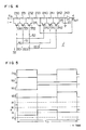
filter 2 and the demodulating interval of received signal (hereinafter referred to as main receiving operation interval) are related to the BS signal. - As described previously, during the interval that the intermitting receiving channel is tuned to the transmitting station, the delivery of the BS signal is repeated at the predetermined period but in Fig. 2, only one period of the BS signal is illustrated.
- Referring to Fig. 2, a start pulse signal (ST) is a signal generated, in response to the BS signal, from a start pulse
clock signal generator 36 of Fig. 1. This ST signal is so controlled as to rise in synchronism with rise of the BS signal and fall at the expiration of Tco interval. A control operation end pulse signal (END) is so controlled as to rise at the expiration of 13 msec beginning with rise of the BS signal and fall in synchronism with fall of the BS signal. - This END signal is delivered to the aforementioned
input switching circuit 1, which turns on the switch 10 (SIN) during on-state of the signal (END). The END signal is inverted and delviered to the switch 11, thereby turning off the switch 11 (SPL) at that time. During off-state of the END signal, the switch 10 (SIN) is turned off and the switch 11 (SPL) is turned on. - The filter time constant control operation is carried out within an interval Tc1 between the fall of ST signal and the rise of END signal. The main receiving operation starts at ts at which an interval Tc following the rise of BS signal expires and ends at the expiration of interval TL at which the BS signal falls. The interval TL is fixed to 1.3 sec pursuant to the system standard concerning paging radio receivers and the present embodiment agrees to this standard. Pursuant to the system standard, the period, Tp, of the bS signal is also fixed measuring 21 sec and the present embodiment also agrees to this standard in this respect.
- The interval Tc0 indicated in Fig. 2 is required in order that the function of individual circuits connected to the power supplies within the receiver can be stabilized in response to the BS signal, and an interval of 10 msec following the rise of END signal is required for start-up of the other digital circuit than the filter. These intervals may be set to appropriate values in course of filter circuit design or may be set to desired values.
- The operation of each block comprised in the
control logic circuit 3 of Fig. 1 will now be described in greater detail. - Receiving the BS signal, the start pulse
clock signal generator 36 delivers the ST signal for determining the start of the control operation and the standard clock pulse signal (CL1 signal). Atiming signal generator 33 receives these two pulse signals and delivers a clock pulse signal (CL2 signal) for determining the frequency of the standard clock signal PL and a clock pulse signal (CL3 signal) for causing aswitch controller 32 to control the timing for switch control. The standardpulse signal generator 31 responds to the clock pulse CL2 to determine the frequency of the standard pulse signal PL and to the reference voltage Vref to determine the amplitude level of the standard pusle signal PL. - Fig. 6 is a graph useful in explaining the relation between the standard pulse signal P1 and filter characteristics of the
filter 2. In the graph of Fig. 6, abscissa represents the frequency of the input signal to the filter and ordinate represents the output signal level (gain) from the filter. - The
filter 2 has its filter characteristic which varies as shown at state A or B because of variations in resistance, temperature and the like factors as well as manufacture errors in capacitance. Accordingly, the shifting state A or B of filter characteristic must be corrected to a target filter characteristic by controlling the filter time constant. In the present embodiment, the filter time constant is controlled in accordance with results of a comparison between a filter output signal level and a predetermined signal level (VTH). To this end, it is preferable to use as the standard pulse signal PL to be inputted to the filter a signal having such a frequency that the output signal level of the filter is affected greatly by variations in filter characteristic. Therefore, in the present embodiment, the standard pulse signal PL is so designed as to have a frequency in out-target band of the filter. - Further, in the present embodiment, the reference voltage Vref for determining the level of the standard pulse signal PL is also used as that for gain determination in the A/
D converter 4. - For example, the signal level of the standard pulse signal PL can be expressed as
PL = K1 · Vref
where K1 is constant, indicating that the standard pulse signal is a signal proportional to the reference voltage Vref. On the other hand, a signal PL′ delivered out of the A/D converter 4 has a signal level expressed as
PL′ = G · VFOUT
where G is constant and VFOUT is filter output voltage, indicating that the signal PL′ is proportional to the signal level of VFOUT. - It is to be noted that the relation between Vref supplied to the A/
D converter 4 and constant G can be expressed by a formula of G = K′ · 1/Vref where K′ is constant. When noticing that the output level of the signal is given by VFOUT = K2 · PL where K2 is constant, the aforementioned latter equation is reduced as follows:
PL′ = G · VFOUT
= G · K2 · PL
= K′ · 1/Vref · K1 · Vref · K2
= K′ · K1 · K2
indicating that the reference voltage Vref has no influence upon the signal PL′. Accordingly, by using the same reference voltage Vref in common for the standardpulse signal generator 31 and A/D converter, the influence of errors interfering with Vref can be cancelled out. - In order to on/off control switches associated with capacitors (C's) 211 to 213 and 221 to 223 used for time constant control (hereinafter simply referred to as "on/off control capacitors"), the
switch controller 32 delivers switch drive signals SD1, SD2 and SD3 and the aforementioned END signal. Timings for these signals are determined by the input clock CL3. The "H" or "L" state of the switch drive signals SD1, SD2 and SD3 ("H" for turn-on of switch and "L" for turn-off of switch) is sequentially determined in accordance with the "H" or "L" polarity of a decision output signal THO of acomparator 35. Alevel detector 34 detects a peak to peak value (Vp-p) from AC amplitude of the standard pulse signal PL′ delivered out of the A/D converter 4 and delivers the detected value to thecomparator 35. The reason why the Vp-p value is detected is that the PL′ signal sometimes contains a DC offset component due to anamplifier 22 comprised in thefiller 2 and a level decision error due to this component must be prevented. Thecomparator 35 delviers "H" when the level deteection output Vp-p value is higher than a threshold value VTH but "1" when lower. - As shown in Fig. 1, the
filter 2 includes a resistor (R) 20 connected to the input signal line (FIN), a first stage filter comprised of a plurality ofcapacitors 210 to 213 connected in parallel to the output end of theresistor 20, aresistor 21 and a second stage filter comprised of a plurality ofcapacitors 220 to 223. Especially, for capacitor connection control, thecapacitors 211 to 213 are associated with switches (SC's) 311 to 313, respectively, and thecapacitors 221 to 223 are associated withswitches 321 to 323. - Three bits are needed for control of the filter time constant. More specifically, the
capacitors capacitors capacitors - A ratio of capacitance among the capacitors to be on/off controlled by the first to third bits is set to be 4:2:1 so that a ratio of 2:1 may be set up between sequential capacitors. More specifically, the
capacitors capacitors 212 and 222 a sum capacitance of 2(pF) and thecapacitors 213 and 223 a sum capacitance of 1(pF). By setting the capacitance ratio among the capacitors in the manner as above, the three control bits can be used to control the capacitance in unit of a minimum controllable capacitor capacitance of 1(pF) within a control range of 7(pF). Accordingly, given that the fixedcapacitors - Referring now to Fig. 3, the relation between the filter time constant control operation and the previously-described clock signals CL1 to CL3 and switch drive signals SD1 to SD3 will now be described. For convenience sake, an example will be explained where the filter time constant control is carried out to set the filter capacitance to 15(pF).
- In synchronism with fall of the aforementioned start pulse signal (ST signal), the start pulse
clock signal generator 36 delivers the clock pulse CL1 having a period of 125 µsec. Thetiming signal generator 33 references this clock pulse C1 to deliver the clock pulse CL2 having a period of 250 µsec and the clock pulse CL3 having a period of 1 msec. The standard pulse signal PL delivered out of the standardpulse signal generator 31 is a rectangular wave having a frequency coincident with that of CL2. At the timing for control start, the switch drive signals SD1, SD2 and SD3 are all rendered "H", with the result that theswitches 311 to 313 and 321 to 323 are all rendered "ON". At the first rise of CL3, the signal SD1 is rendered "L" to bring the correspondingswitches - Since in this example the VTH is so set as to make the filter capacitance 15(pF), the output value THO of the
comparator 35 is "H". As a result, theswitch controller 32 sets the switch drive pulse SD1 to "H". Subsequently, at the second rise of CL3, the signal SD2 is set to "L". As a result, theswitches switch controller 32 sets the SD2 to "L" in order to render theswitches switches switch controller 32 sets the SD3 to "H" in order to render theswitches input switching circuit 1, thereby bringing about the state where the main signal reception can be permitted. - As described above, by setting the switching capacitors of the filter sequentially from the maximum bit to the minimum bit, the control operation of all time constants can be completed when setting of the minimum bit ends.
- The total filter capacitance Cc can be changed through the above capacitor control operation as shown at the bottom section in Fig. 3. At the end of the control operation, the value of Cc measures 15(pF) within the adjusting range of from 10 to 17(pF). In the present embodiment, the control switches 311
t - Further, in the foregoing embodiment, the time constant of the
filter 2 is controlled by switching the capacitor capacitance but alternatively the time constant control can be effected by switching resistance. - Fig. 4 is a circuit diagram showing a filter construction in which the resistance is changed. As shown, in the filter designated by 2′, an input line (FIN) of the filter is connected to the
input switching circuit 1 and an output terminal (FOUT) is connected to the A/D converter 4 as in the case of thefilter 2 of Fig. 1, andinternal resistors 230 to 232 and 240 to 242 are controlled for short-circuiting by means of associatedswitches 330 to 332 and 340 to 342. - The
filter 2′ is a low-pass filter including a first stage filter comprised ofresistors 230 to 233 connected in series with the input line (FIN) and acapacitor 24, and a second stage filter comprised ofresistors 240 to 243 connected in series and acapacitor 25. Theresistors - Since in this embodiment the individual resistance are short-circuited when the SD1′ to SD3′ signals are rendered "H", the polarity of the SD1′ to SD3′ msut be inverted as compared to that of the SD1 to SD3 signals explained in connection with Fig. 3.
- When the time constant control is carried out using the
filter 2′, the switch drive signals (SD1′ to SD3′ signals) and the total resistance, R, are changed as shown in Fig. 5. The behavior shown in Fig. 5 resembles in principle that in Fig. 3 and will not be described herein. - In the foregoing embodiments, the filter time constant control system of the invention has been described as applied to the paging radio receiver which performs the receiving operation periodically. However, the filter time constant control system according to the invention may also be applied to an apparatus wherein a filter is comprised in the apparatus, the time constant of the filter is controlled for correction and thereafter the controlled and corrected filter is used for an intended signal processing. For example, a radio, a television and a communication terminal may be enumerated as this type of apparatus. In this case, the connective relation between the
filter 2 and time constant control circuit must be changed slightly. For example, when the filter output signal takes the form of an analog value, the output signal of thefilter 2 of Fig. 1 may be inputted directly to thelevel detector 34 and connected to output circuits handling the filter analog output signal as it is. - The foregoing embodiments have been described as directed to automatic correction of manufacture errors of the filter time constant but the filter in these embodiments may readily be used as a variable filter if the threshold voltage VTH of the Fig. 1 comparator or the level or frequency of the standard pulse signal PL is adjusted.
- A second embodiment of the invention as applied to the paging radio receiver will now be described.
- The foregoing embodiments use the standard pulse signal of the predetermined frequency and level as the signal inputted to the filter during the time constant control interval. Contrary to this, in the second embodiment, a triangular wave is generated using time constant determining elements of a filter, the output level of the triangular wave is compared with a fixed reference level, and the filter time constant is controlled and switched in accordance with the magnitude relation between the compared levels.
- Fig. 7 is a diagram for explaining the second embodiment. Referring to Fig. 7, a
triangular wave generator 9 includes an input switching circuit for generating a triangular wave and a switch circuit which is on/off controlled to connect/disconnect the opposition ends of capacitors. Denoted by 30 is a control logic circuit for controlling the time constant of thefilter 2. The function and operation ofcomponents - Applied to a switch (SPL) 11 of the input switching circuit is a DC voltage VB. A switch (SO) 92 has one end grounded and the other end connected to the input of an
amplifier 22 provided forcapacitors 220 to 223 of afilter 2. - The
control logic circuit 30 has no circuit corresponding to the standardpulse signal generator 31 of Fig. 1. In the second embodiment, atiming signal generator 330 delivers a pulse (SWP) 500 for on/off controlling the switch (SO) 92 of thetriangular wave generator 9. An output signal (FOUT) 47 of thefilter 2 is applied directly to acomparator 35. Accordingly, in contrast to the digital type comparator in the first embodiment, the comparator in the second embodiment is of an analog type. The remaining portion of thecontrol logic circuit 30 is the same as that of thecircuit 3 in the first embodiment and will not be described herein. - Alternatively, the
triangular wave generator 9 may be connected, for example, between a resistor (R) 21 and acapacitor 213 in thefilter 2. - Since in the first embodiment the capacitor corresponding to each bit is rendered "OFF" at the rise of CL3 and there results a transient response, it takes 1 msec (corresponding to 4 periods of the standard pulse signal) for the level of standard pulse signal PL to become stable, totalling 3 msec for 3 bits. However, in the second embodiment, the opposite ends of the capacitor are short-circuited at the rate of one period of the signal by means of the switch (SO) 90 to reset the level and therefore the influence of the transient response becomes negligible. Accordingly, when the period of the switch drive pulse SWP (Fig. 7) is designed to be identical to that of the standard pulse signal PL (Fig. 3), the period of CL3 (Fig. 7) becomes 1/4 of the period of CL3 (Fig. 3) and the total time TC1 required for time constant control measures 0.75 msec which is 1/4 of 3 msec.
- Referring now to Fig. 8, signal waveforms at various points in the second embodiment will be described. Waves ST, CL1, CL3 and END in Fig. 8 resemble those in Fig. 3 and their description will be omitted.
- In Fig. 8, the drive pulse SWP is to on/off control the switch (SO) 92 and in this example the switch is turned on with high level "H" of the drive pulse and turned off with low level "L" of the drive pulse. The output signal FOUT of the
filter 2 stands for an input signal to thecomparator 35. Simultaneously indicated on ordinate of a graph section indicating the FOUT waveform are a threshold voltage VTH of thecomparator 35 and a DC voltage VB. The output signal, THO, of thecomparator 35 is rendered high level "H" when the level of the input signal (FOUT) 47 is higher than the threshold VTH but is rendered low level "L" when lower. - These waveforms take place in the case where the total capacitance of the capacitors within the filter is set to 15(pF) as in the case of Fig. 3 corresponding to the first embodiment.
- The signals SD1, SD2 and SD3 start falling at the same timing or phase as that in the first embodiment (see Fig. 3) but start rising at earlier timings than those in the first embodiment (see Fig. 3). For these reasons, the waveform of the total capacitance Cc of the capacitors varies differently from that shown in Fig. 3 but the ultimate total capacitance Cc of the capacitors can also be converged to 15(pF).
- As is clear from the description of the foregoing embodiments, according to the filter time constant control system of the invention, the filter capable of controlling the time constant can be reduced in its circuit area and power consumption.
- Specified effects can be enumerated as below.
- The first effect is such that the power consumption reduction can be attained by separating the time constant control operation from the normal operation and completing the former operation within a short interval of time. As described previously, while the received signal demodulating interval of the paging radio receiver is 1300 ms, the time constant control interval (Tc1) of the filter is 3 msec. Thus, the time ratio of the time constant control interval to the demodulating interval of the received signal is about 0.23%, indicating that power consumption during the time constant control interval can be reduced to a level which is almost negligible.
- The second effect is such that the invention does not require the conventional artificial filter and the circuit area and power consumption can be reduced correspondingly. This is because in the present invention, the standard pulse signal is applied directly to the filter used for filtering the received signal without resort to the aritificial filter and the output level of the filter is compared with the reference level to detect the time constant difference.
- The third effect is such that there is no need of using a filter including variable capacitor diodes as time constant control elements and therefore no high control voltage is required, thereby ensuring reduction in power supply voltage. In addition, such a differential active filter as used in the case where ON resistance of D-MOS is utilized can be unneeded and therefore the circuit area can be reduced.
- The fourth effect is such that the control time can be reduced by setting a ratio of capacitance (or resistance) among capacitors (resistors) used as time constant control elements to 4:2:1 to set up a ratio of 2:1 between sequential elements and by shifting the setting operation sequentially from the maximum bit to the minimum bit during the time constant controlling. In the embodiments, the number of bits is 3 and the time constant control operation can be completed through three-times setting operations (about 3 msec).
Claims (11)
inputting to said filter a periodical signal (PL) having a predetermined frequency and a predetermined signal level during a predetermined interval preceding each filtering operation;
switching the time constant of said filter by a predetermined number of times in accordance with an output signal (FOUT) from said filter; and
performing filtering of the input signal after completion of switching of the time constant of said filter.
said filter having its time constant switchable stepwise;
a controller (3) for controlling the time constant of said filter; and
a selector (1), responsive to a command (END) from said controller, for selectively inputting to said filter either said input signal or a periodical signal (PL) having a predetermined frequency and a predetermined signal level,
wherein said controller applies said periodical signal to said filter in advance of each filtering operation and responds to an output signal (FOUT) from said filter to control the time constant thereof.
said filter having its time constant switchable stepwise;
a controller (30) for controlling the time constant of said filter; and
a selector (9), responsive to a command from said controller, for selectively connecting to said filter either an input line of said input signal or a constant voltage source (VB) for causing said filter to generate a triangular wave (FOUT),
wherein said controller connects said constant voltage source to said filter in advance of each filtering operation and responds to a triangular-wave output signal from said filter to control the time constant thereof.
inputting to a filter (2) within said radio receiver a periodical signal having a predetermined frequency and a predetermined signal level and controlling switching of the time constant of said filter during a first time zone within each operation interval; and
filtering, demodualting and delivering said received signal during a second time zone after completion of said time constant control.
a filter (2) operable for filtering an input signal and having its time constant switchable stepwise;
a demodualting circuit (6) for demodulating and delivering an ouput signal (FOUT) from said filter;
a controller (3) for controlling the time constant of said filter; and
an input switching circuit (1), responsive to a command from said controller, for selectively inputting to said filter either the signal from said transmitting station or a periodical signal having a predetermined frequency,
wherein said controller performs control for applying said periodical signal to said filter so as to control the time constant of said filter in accordance with the output signal from said filter during a first time zone within each operation interval and for filtering, demodulating and delivering the signal from said transmitting station during a second time zone after completion of said time constant control.
a filter (2) operable for filtering an input signal and having its time constant switchable stepwise;
a demodulating circuit (6) for demodulating and delivering an output signal (FOUT) from said filter;
a controller (30) for controlling the time constant of said filter; and
a selector (9), responsive to a command from said controller, for selectively connecting to said filter either an input line of a received signal from said transmitting station or a constant voltage source (VB) for causing said filter to generate a triangular wave,
wherein said controller performs control for applying a periodical signal to said filter so as to control the time constant of said filter in accordance with the triangular-wave output signal from said filter during a first time zone within each operation interval and for filtering, demodulating and delivering the signal from said transmitting station during a second time zone after completion of said time constant control.
a filter (2) operable for filtering an input signal and having its time constant switchable stepwise;
an analog-digital converter (4) for analog-digital conversion of an output signal from said filter;
a demodulating circuit (6) for demodulating and delivering an output signal from said analog-digital converter;
a controller (3) for controlling the time constant of said filter; and
an input switching circuit (1), responsive to a command from said controller, for selectively inputting to said filter either the signal from said transmitting station or a periodical signal having a predetermined frequency,
wherein said controller performs control for applying said periodical signal to said filter so as to control the time constant of said filter in accordance with the output signal from said analog-digital converter during a first time zone within each operation interval and for filtering, demodulating and delivering the signal from said transmitting station during a second time zone after completion of said time constant control.
Applications Claiming Priority (2)
| Application Number | Priority Date | Filing Date | Title |
|---|---|---|---|
| JP260027/89 | 1989-10-06 | ||
| JP26002789 | 1989-10-06 |
Publications (3)
| Publication Number | Publication Date |
|---|---|
| EP0421423A2 true EP0421423A2 (en) | 1991-04-10 |
| EP0421423A3 EP0421423A3 (en) | 1991-11-06 |
| EP0421423B1 EP0421423B1 (en) | 1997-01-08 |
Family
ID=17342288
Family Applications (1)
| Application Number | Title | Priority Date | Filing Date |
|---|---|---|---|
| EP90119053A Expired - Lifetime EP0421423B1 (en) | 1989-10-06 | 1990-10-04 | Method of controlling filter time constant and filter circuit having the time constant control function based on the method |
Country Status (4)
| Country | Link |
|---|---|
| US (1) | US5392456A (en) |
| EP (1) | EP0421423B1 (en) |
| JP (1) | JP3070758B2 (en) |
| DE (1) | DE69029637T2 (en) |
Cited By (5)
| Publication number | Priority date | Publication date | Assignee | Title |
|---|---|---|---|---|
| EP0851378A1 (en) * | 1996-12-30 | 1998-07-01 | Datalogic S.P.A. | Method and device for measuring and regulating a time constant of an electronic circuit forming part of an optical code reader |
| EP0863623A3 (en) * | 1997-03-04 | 1999-09-22 | Nec Corporation | Device and method for controlling frequency characteristic of a filter |
| WO2001024363A3 (en) * | 1999-09-28 | 2001-10-18 | Koninkl Philips Electronics Nv | An integrated circuit having a filter with charge balancing scheme to reduce transient disturbances |
| WO2002091573A1 (en) * | 2001-05-03 | 2002-11-14 | Infineon Technologies Ag | Method and device for adjusting an active filter |
| EP2197109A1 (en) * | 2008-12-15 | 2010-06-16 | STMicroelectronics Srl | Integrated programmable gain amplifier circuit and system including said circuit |
Families Citing this family (23)
| Publication number | Priority date | Publication date | Assignee | Title |
|---|---|---|---|---|
| US5499392A (en) * | 1994-07-19 | 1996-03-12 | Matsushita Communication Industrial Corporation Of America | Filter having a variable response time for filtering an input signal |
| US5796545A (en) * | 1995-06-07 | 1998-08-18 | Sgs-Thomson Microelectronics, Inc. | Device and method for calibrating a time constant of one or more filter circuits |
| US5982228A (en) * | 1995-07-14 | 1999-11-09 | Lucent Technologies Inc | Frequency tuning apparatus and method for continuous-time filters |
| DE69707209T2 (en) * | 1996-02-05 | 2002-06-27 | Koninklijke Philips Electronics N.V., Eindhoven | RECEIVING MULTI-STANDARD SIGNALS |
| US6118331A (en) * | 1997-06-20 | 2000-09-12 | Texas Instruments Incorporated | Method and system for a digital filter having improved settling time |
| US6535075B2 (en) * | 1999-12-16 | 2003-03-18 | International Business Machines Corporation | Tunable on-chip capacity |
| US6630860B1 (en) | 2000-09-20 | 2003-10-07 | Applied Micro Circuits Corporation | Programmable phase locked-loop filter architecture for a range selectable bandwidth |
| US6333674B1 (en) * | 2001-03-15 | 2001-12-25 | Kim Dao | Feedback stabilization apparatus and methods |
| US6856925B2 (en) * | 2001-10-26 | 2005-02-15 | Texas Instruments Incorporated | Active removal of aliasing frequencies in a decimating structure by changing a decimation ratio in time and space |
| JP2003198404A (en) * | 2001-12-26 | 2003-07-11 | Matsushita Electric Ind Co Ltd | Direct conversion receiver, mobile radio using the same, and method of receiving RF signal |
| US7024254B2 (en) * | 2002-02-14 | 2006-04-04 | Johnson Controls Technology Company | Method for controlling a discrete system |
| US7761067B1 (en) * | 2003-05-15 | 2010-07-20 | Marvell International Ltd. | Iterative filter circuit calibration |
| US6965275B2 (en) * | 2004-02-13 | 2005-11-15 | Infineon Technologies Ag | Method and apparatus for tuning a filter |
| DE102004026148B4 (en) * | 2004-05-28 | 2010-06-24 | Advanced Micro Devices, Inc., Sunnyvale | Digitally controlled filter tuning for WLAN communication devices |
| DE102005006345A1 (en) * | 2005-02-11 | 2006-08-24 | Rohde & Schwarz Gmbh & Co. Kg | PLL synthesizer with improved VCO pre-tuning |
| US7190213B2 (en) * | 2005-03-25 | 2007-03-13 | Freescale Semiconductor, Inc. | Digital time constant tracking technique and apparatus |
| JP4660248B2 (en) * | 2005-03-31 | 2011-03-30 | パナソニック株式会社 | Filter automatic adjustment device, filter adjustment method, and mobile phone system |
| US7583948B2 (en) * | 2005-04-28 | 2009-09-01 | Kabushiki Kaisha Toshiba | Time constant automatic adjusting circuit, filter circuit system, and method of automatically adjusting time constant |
| US7596193B2 (en) | 2005-11-09 | 2009-09-29 | Via Telecom, Inc. | Variable bandwidth automatic gain control |
| CN101953073A (en) * | 2008-01-18 | 2011-01-19 | 松下电器产业株式会社 | Ramp wave output circuit, analog-to-digital conversion circuit, and camera |
| FR2941576B1 (en) * | 2009-01-28 | 2016-07-15 | St Wireless Sa | METHOD AND SYSTEM FOR CALIBRATING AN INTEGRATED TIME CONSTANT, AND INTEGRATED CIRCUIT PROVIDED WITH SUCH A SYSTEM |
| US8791767B2 (en) * | 2010-10-29 | 2014-07-29 | Qualcomm Incorporated | Package inductance compensating tunable capacitor circuit |
| CN118283875B (en) * | 2024-06-03 | 2024-10-22 | 佛山市伊戈尔电子有限公司 | Filter circuit for dimming circuit |
Family Cites Families (11)
| Publication number | Priority date | Publication date | Assignee | Title |
|---|---|---|---|---|
| DE1163921B (en) * | 1958-09-26 | 1964-02-27 | Siemens Ag | Arrangement for changing the time constants of RC elements |
| NL7205691A (en) * | 1972-04-27 | 1973-05-25 | ||
| US4181893A (en) * | 1975-06-26 | 1980-01-01 | Motorola, Inc. | Battery saver for a tone coded signalling system |
| JPS588770B2 (en) * | 1976-04-21 | 1983-02-17 | 株式会社島津製作所 | filter device |
| US4392068A (en) * | 1981-07-17 | 1983-07-05 | General Electric Company | Capacitive commutating filter |
| DE3347132C1 (en) * | 1983-12-27 | 1985-07-04 | Deutsche Thomson-Brandt Gmbh, 7730 Villingen-Schwenningen | Automatic adjustment system for a tuner of a television receiver |
| JPS60214617A (en) * | 1984-04-11 | 1985-10-26 | Hitachi Ltd | Filter integrated circuit |
| GB2190255B (en) * | 1986-04-30 | 1989-11-29 | Philips Electronic Associated | Electrical filter |
| JPH0787332B2 (en) * | 1986-07-18 | 1995-09-20 | 株式会社東芝 | Automatic time constant adjustment circuit for filter circuit |
| US5058204A (en) * | 1989-08-02 | 1991-10-15 | Motorola, Inc. | Synthesized selective call receiver having variable characteristics |
| US5101509A (en) * | 1990-09-14 | 1992-03-31 | Ford Motor Company | Rf filter alignment using digital processor clock |
-
1990
- 1990-10-03 US US07/592,340 patent/US5392456A/en not_active Expired - Fee Related
- 1990-10-04 EP EP90119053A patent/EP0421423B1/en not_active Expired - Lifetime
- 1990-10-04 DE DE69029637T patent/DE69029637T2/en not_active Expired - Fee Related
- 1990-10-05 JP JP02266240A patent/JP3070758B2/en not_active Expired - Fee Related
Cited By (9)
| Publication number | Priority date | Publication date | Assignee | Title |
|---|---|---|---|---|
| EP0851378A1 (en) * | 1996-12-30 | 1998-07-01 | Datalogic S.P.A. | Method and device for measuring and regulating a time constant of an electronic circuit forming part of an optical code reader |
| EP0863623A3 (en) * | 1997-03-04 | 1999-09-22 | Nec Corporation | Device and method for controlling frequency characteristic of a filter |
| US6122496A (en) * | 1997-03-04 | 2000-09-19 | Nec Corporation | Device and method for controlling frequency characteristic of a filter |
| WO2001024363A3 (en) * | 1999-09-28 | 2001-10-18 | Koninkl Philips Electronics Nv | An integrated circuit having a filter with charge balancing scheme to reduce transient disturbances |
| WO2002091573A1 (en) * | 2001-05-03 | 2002-11-14 | Infineon Technologies Ag | Method and device for adjusting an active filter |
| US7116159B2 (en) | 2001-05-03 | 2006-10-03 | Infineon Technologies Ag | Method and apparatus for adjusting an active filter |
| EP2197109A1 (en) * | 2008-12-15 | 2010-06-16 | STMicroelectronics Srl | Integrated programmable gain amplifier circuit and system including said circuit |
| ITRM20080664A1 (en) * | 2008-12-15 | 2010-06-16 | St Microelectronics Srl | INTEGRATED CIRCUIT BUILDING AMPLIFICATION CIRCUIT AND SYSTEM INCLUDING THE CIRCUIT |
| US8044718B2 (en) | 2008-12-15 | 2011-10-25 | Stmicroelectronics S.R.L. | Integrated programmable gain amplifier circuit and system including the circuit |
Also Published As
| Publication number | Publication date |
|---|---|
| EP0421423B1 (en) | 1997-01-08 |
| DE69029637T2 (en) | 1997-07-31 |
| DE69029637D1 (en) | 1997-02-20 |
| JP3070758B2 (en) | 2000-07-31 |
| US5392456A (en) | 1995-02-21 |
| EP0421423A3 (en) | 1991-11-06 |
| JPH03209910A (en) | 1991-09-12 |
Similar Documents
| Publication | Publication Date | Title |
|---|---|---|
| US5392456A (en) | Method of controlling filter time constant and filter circuit having the time constant control function based on the method | |
| US5752174A (en) | Radio receiver with automatic adjustment of oscillation frequencies | |
| US5450621A (en) | Radio receiver with digital control loop for coarse frequency acquisition and analog control loop for frequency lock-in | |
| JPH06195032A (en) | Correction circuit of deflection waveform | |
| KR100445320B1 (en) | Pulse counting demodulators | |
| KR100240127B1 (en) | Delay Automatic Gain Control Circuit | |
| KR960001760B1 (en) | Circuit synchronized by a signal at a deflection frequency | |
| US7062244B2 (en) | Speed-up mode implementation for direct conversion receiver | |
| US3946329A (en) | Electronic automatic frequency tuning system | |
| US7075372B2 (en) | Programmable automatic signal amplitude control circuit | |
| EP1148645A2 (en) | Phase shift circuit and fm detector circuit | |
| US4891708A (en) | Voltage superposing circuit for an electronic tuner | |
| KR20040078691A (en) | Semiconductor integrated circuit for radio apparatus and radio communication apparatus | |
| KR910001827Y1 (en) | Auto-tunning circuit of satellite broadcast | |
| KR200322195Y1 (en) | Automatic Gain Control Circuit of Tuner | |
| KR20010095152A (en) | Phase shift circuit and fm detecting circuit | |
| JP2005094553A (en) | Digital tuner | |
| KR0153083B1 (en) | Tuner regulation device | |
| KR100315345B1 (en) | Voltage generating circuit for fine tuning by automatic control | |
| JPH0349472Y2 (en) | ||
| JP4075890B2 (en) | Pulse count demodulator | |
| KR950007499Y1 (en) | Programmable Frequency Detection Circuit | |
| EP0798850B1 (en) | Improvements in or relating to radio receivers | |
| EP0583846B1 (en) | Receiver for receiving high-frequency signals | |
| KR19980054951U (en) | Tuner |
Legal Events
| Date | Code | Title | Description |
|---|---|---|---|
| PUAI | Public reference made under article 153(3) epc to a published international application that has entered the european phase |
Free format text: ORIGINAL CODE: 0009012 |
|
| AK | Designated contracting states |
Kind code of ref document: A2 Designated state(s): DE GB |
|
| PUAL | Search report despatched |
Free format text: ORIGINAL CODE: 0009013 |
|
| AK | Designated contracting states |
Kind code of ref document: A3 Designated state(s): DE GB |
|
| 17P | Request for examination filed |
Effective date: 19920227 |
|
| 17Q | First examination report despatched |
Effective date: 19940824 |
|
| GRAG | Despatch of communication of intention to grant |
Free format text: ORIGINAL CODE: EPIDOS AGRA |
|
| GRAH | Despatch of communication of intention to grant a patent |
Free format text: ORIGINAL CODE: EPIDOS IGRA |
|
| GRAH | Despatch of communication of intention to grant a patent |
Free format text: ORIGINAL CODE: EPIDOS IGRA |
|
| GRAA | (expected) grant |
Free format text: ORIGINAL CODE: 0009210 |
|
| AK | Designated contracting states |
Kind code of ref document: B1 Designated state(s): DE GB |
|
| REF | Corresponds to: |
Ref document number: 69029637 Country of ref document: DE Date of ref document: 19970220 |
|
| PLBE | No opposition filed within time limit |
Free format text: ORIGINAL CODE: 0009261 |
|
| STAA | Information on the status of an ep patent application or granted ep patent |
Free format text: STATUS: NO OPPOSITION FILED WITHIN TIME LIMIT |
|
| 26N | No opposition filed | ||
| PGFP | Annual fee paid to national office [announced via postgrant information from national office to epo] |
Ref country code: GB Payment date: 20011008 Year of fee payment: 12 |
|
| PGFP | Annual fee paid to national office [announced via postgrant information from national office to epo] |
Ref country code: DE Payment date: 20011230 Year of fee payment: 12 |
|
| REG | Reference to a national code |
Ref country code: GB Ref legal event code: IF02 |
|
| PG25 | Lapsed in a contracting state [announced via postgrant information from national office to epo] |
Ref country code: GB Free format text: LAPSE BECAUSE OF NON-PAYMENT OF DUE FEES Effective date: 20021004 |
|
| PG25 | Lapsed in a contracting state [announced via postgrant information from national office to epo] |
Ref country code: DE Free format text: LAPSE BECAUSE OF NON-PAYMENT OF DUE FEES Effective date: 20030501 |
|
| GBPC | Gb: european patent ceased through non-payment of renewal fee |
Effective date: 20021004 |