EP0448614B1 - Method of optimizing a conductor-path layout for the printing head of an ink printing device, and a conductor-path layout for such a printing head - Google Patents
Method of optimizing a conductor-path layout for the printing head of an ink printing device, and a conductor-path layout for such a printing head Download PDFInfo
- Publication number
- EP0448614B1 EP0448614B1 EP19900900866 EP90900866A EP0448614B1 EP 0448614 B1 EP0448614 B1 EP 0448614B1 EP 19900900866 EP19900900866 EP 19900900866 EP 90900866 A EP90900866 A EP 90900866A EP 0448614 B1 EP0448614 B1 EP 0448614B1
- Authority
- EP
- European Patent Office
- Prior art keywords
- conductor
- conductor paths
- transition structure
- zones
- paths
- Prior art date
- Legal status (The legal status is an assumption and is not a legal conclusion. Google has not performed a legal analysis and makes no representation as to the accuracy of the status listed.)
- Expired - Lifetime
Links
- 238000000034 method Methods 0.000 title claims description 6
- 238000007639 printing Methods 0.000 title description 6
- 239000004020 conductor Substances 0.000 claims abstract description 88
- 238000010438 heat treatment Methods 0.000 claims abstract description 34
- 230000007704 transition Effects 0.000 claims abstract description 31
- 239000010409 thin film Substances 0.000 claims abstract description 14
- 239000000758 substrate Substances 0.000 claims abstract description 12
- 239000008186 active pharmaceutical agent Substances 0.000 description 6
- XAGFODPZIPBFFR-UHFFFAOYSA-N aluminium Chemical compound [Al] XAGFODPZIPBFFR-UHFFFAOYSA-N 0.000 description 3
- 229910052782 aluminium Inorganic materials 0.000 description 3
- 238000005516 engineering process Methods 0.000 description 1
- 230000008020 evaporation Effects 0.000 description 1
- 238000001704 evaporation Methods 0.000 description 1
- 238000007641 inkjet printing Methods 0.000 description 1
- 238000005457 optimization Methods 0.000 description 1
- 238000002407 reforming Methods 0.000 description 1
- 230000004304 visual acuity Effects 0.000 description 1
Images


Classifications
-
- H—ELECTRICITY
- H05—ELECTRIC TECHNIQUES NOT OTHERWISE PROVIDED FOR
- H05K—PRINTED CIRCUITS; CASINGS OR CONSTRUCTIONAL DETAILS OF ELECTRIC APPARATUS; MANUFACTURE OF ASSEMBLAGES OF ELECTRICAL COMPONENTS
- H05K1/00—Printed circuits
- H05K1/02—Details
- H05K1/0213—Electrical arrangements not otherwise provided for
- H05K1/0263—High current adaptations, e.g. printed high current conductors or using auxiliary non-printed means; Fine and coarse circuit patterns on one circuit board
- H05K1/0265—High current adaptations, e.g. printed high current conductors or using auxiliary non-printed means; Fine and coarse circuit patterns on one circuit board characterized by the lay-out of or details of the printed conductors, e.g. reinforced conductors, redundant conductors, conductors having different cross-sections
-
- B—PERFORMING OPERATIONS; TRANSPORTING
- B41—PRINTING; LINING MACHINES; TYPEWRITERS; STAMPS
- B41J—TYPEWRITERS; SELECTIVE PRINTING MECHANISMS, i.e. MECHANISMS PRINTING OTHERWISE THAN FROM A FORME; CORRECTION OF TYPOGRAPHICAL ERRORS
- B41J2/00—Typewriters or selective printing mechanisms characterised by the printing or marking process for which they are designed
- B41J2/005—Typewriters or selective printing mechanisms characterised by the printing or marking process for which they are designed characterised by bringing liquid or particles selectively into contact with a printing material
- B41J2/01—Ink jet
- B41J2/135—Nozzles
- B41J2/14—Structure thereof only for on-demand ink jet heads
- B41J2/14016—Structure of bubble jet print heads
- B41J2/14072—Electrical connections, e.g. details on electrodes, connecting the chip to the outside...
-
- B—PERFORMING OPERATIONS; TRANSPORTING
- B41—PRINTING; LINING MACHINES; TYPEWRITERS; STAMPS
- B41J—TYPEWRITERS; SELECTIVE PRINTING MECHANISMS, i.e. MECHANISMS PRINTING OTHERWISE THAN FROM A FORME; CORRECTION OF TYPOGRAPHICAL ERRORS
- B41J2/00—Typewriters or selective printing mechanisms characterised by the printing or marking process for which they are designed
- B41J2/005—Typewriters or selective printing mechanisms characterised by the printing or marking process for which they are designed characterised by bringing liquid or particles selectively into contact with a printing material
- B41J2/01—Ink jet
- B41J2/135—Nozzles
- B41J2/16—Production of nozzles
- B41J2/1601—Production of bubble jet print heads
-
- B—PERFORMING OPERATIONS; TRANSPORTING
- B41—PRINTING; LINING MACHINES; TYPEWRITERS; STAMPS
- B41J—TYPEWRITERS; SELECTIVE PRINTING MECHANISMS, i.e. MECHANISMS PRINTING OTHERWISE THAN FROM A FORME; CORRECTION OF TYPOGRAPHICAL ERRORS
- B41J2/00—Typewriters or selective printing mechanisms characterised by the printing or marking process for which they are designed
- B41J2/005—Typewriters or selective printing mechanisms characterised by the printing or marking process for which they are designed characterised by bringing liquid or particles selectively into contact with a printing material
- B41J2/01—Ink jet
- B41J2/135—Nozzles
- B41J2/16—Production of nozzles
- B41J2/1621—Manufacturing processes
- B41J2/1623—Manufacturing processes bonding and adhesion
-
- B—PERFORMING OPERATIONS; TRANSPORTING
- B41—PRINTING; LINING MACHINES; TYPEWRITERS; STAMPS
- B41J—TYPEWRITERS; SELECTIVE PRINTING MECHANISMS, i.e. MECHANISMS PRINTING OTHERWISE THAN FROM A FORME; CORRECTION OF TYPOGRAPHICAL ERRORS
- B41J2202/00—Embodiments of or processes related to ink-jet or thermal heads
- B41J2202/01—Embodiments of or processes related to ink-jet heads
- B41J2202/11—Embodiments of or processes related to ink-jet heads characterised by specific geometrical characteristics
-
- H—ELECTRICITY
- H05—ELECTRIC TECHNIQUES NOT OTHERWISE PROVIDED FOR
- H05K—PRINTED CIRCUITS; CASINGS OR CONSTRUCTIONAL DETAILS OF ELECTRIC APPARATUS; MANUFACTURE OF ASSEMBLAGES OF ELECTRICAL COMPONENTS
- H05K2201/00—Indexing scheme relating to printed circuits covered by H05K1/00
- H05K2201/07—Electric details
- H05K2201/0776—Resistance and impedance
- H05K2201/0784—Uniform resistance, i.e. equalizing the resistance of a number of conductors
-
- H—ELECTRICITY
- H05—ELECTRIC TECHNIQUES NOT OTHERWISE PROVIDED FOR
- H05K—PRINTED CIRCUITS; CASINGS OR CONSTRUCTIONAL DETAILS OF ELECTRIC APPARATUS; MANUFACTURE OF ASSEMBLAGES OF ELECTRICAL COMPONENTS
- H05K2201/00—Indexing scheme relating to printed circuits covered by H05K1/00
- H05K2201/09—Shape and layout
- H05K2201/09209—Shape and layout details of conductors
- H05K2201/09654—Shape and layout details of conductors covering at least two types of conductors provided for in H05K2201/09218 - H05K2201/095
- H05K2201/09727—Varying width along a single conductor; Conductors or pads having different widths
Definitions
- the invention relates to a method for optimizing a conductor track arrangement for a write head in ink printing devices and a conductor track arrangement for such a write head in accordance with the preambles of claims 1 and 2.
- each individual heating element has its own electrical outward and return line in the form of metallic conductor tracks, preferably made of aluminum, which, for the purpose of external electrical contacting, are distributed, for example, to individual conductors of a connecting cable over the surface of the thin-film substrate to a connection field to lead.
- the heating elements are arranged in a row with a narrow pitch in an area near the edge of the thin film substrate, and the leads have to be routed to the relatively wide connection field on the opposite side of the thin film substrate in order to make contact with the edges, the different conductor lengths also result in different lead resistances for the individual Heating elements, which leads to the problems mentioned above.
- connection lines starting from the heating elements to be contacted in an area with wide division, in one at a connection of an integrated circuit adjacent area with a narrow division and a transition area connecting these two areas are broken down.
- the connecting lines in the individual areas run parallel to one another and in order to achieve an approximately equal supply resistance of the individual connecting lines, resistance correction zones are provided either only on one side (JP-A-6076355) of the heating elements to be contacted or on both sides (JP-A-612575) of the heating elements.
- the correction zones or line resistance compensation paths are provided by sections of the connecting lines of different widths and lengths only in the areas of the wide division.
- the object on which the invention is based is therefore to specify a method for optimizing a conductor track arrangement for write heads constructed in thin-film technology in ink printing devices, which ensures that the lead resistance for all heating elements is as identical and as low as possible for all heating elements.
- a suitable dimensioning of the transition structure which connects the conductor tracks of narrow division in the area of the heating elements with the conductor tracks of further division in the area of the connection contacts, enables the conductor resistance of the conductor tracks to be the same and lower for all heating elements.
- a dimensioning specification assigns the specified input variables (conductor widths and gap width of the conductor tracks in the two areas) and the gap width in the transition structure to the conductor width in the transition structure as an output variable.
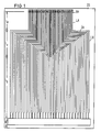
- the reference symbol DS denotes a thin film substrate on which the individual heating elements RH and their supply lines are structured. These supply lines - one forward and one return line per heating element - lead from the heating elements RH located in an edge region of the thin film substrate DS to a connection field AF located on the opposite side of the thin film substrate DS, where the supply lines are contacted to a connecting cable, not shown here. Since on the one hand there must be sufficient space for this contacting and on the other hand the heating elements RH should be arranged relatively small and closely adjacent due to the highest possible resolving power, the conductor tracks on the thin film substrate DS are fanned out.
- the conductor tracks on the thin-film substrate DS in the area of the heating elements RH are divided into conductor tracks of narrow pitch LA and in the area of the connection field AF in conductor tracks further pitch LB.
- a transition structure ÜV connects the interconnects narrow division LA with the conductors further division LB. The lengths of these three areas are also shown in FIG 1 A is the guide length of narrow pitch, 1 V is the length of the transition structure and 1 B is the length of the wire pitch.
- this transition structure ÜV which connects the conductor tracks of narrow division (in the area of the heating elements) with the conductor tracks of further division (in the area of the connection field), an identical and yet small lead resistance can be achieved for all heating dots.
- FIG. 2 shows an enlarged section from FIG. 1 and shows the course of two adjacent conductor tracks L1, L2 in the three areas mentioned.
- the geometric dimensions and the resistance contributions of the individual conductor track sections are shown in FIG. Specifically, these are the width d a , d v and d b of the conductor tracks in the areas of narrow pitch LA, the transition structure ÜV and further pitch LB and the distances s a , s v , s b of two adjacent conductor tracks L1, L2 in the corresponding areas.
- the conductor tracks within the individual areas run parallel to one another, while the conductor tracks of adjacent areas are arranged at right angles to one another.
- the total resistance of a conductor track L i is composed of a resistance component R bi of the conductor track of further division, a resistance component R vi of the transition structure and a resistance component R ai of the conductor joint of narrow division.
- This distance s v is a function of the predetermined parameters distances a , s b and conductor widths d a , d b of the conductor paths in the areas of narrow and wide division and the parameter conductor width d v in the transition area.
- abbreviation c d b ⁇ D a ⁇ (I.e.
- the equation (*) is shown in general form (s v , d v in the units ⁇ c).
- the trace width d v is plotted on the abscissa and the gap width s v on the ordinate.
- the resistance of a supply line R g is made up proportionally of the resistance contributions of the ladder narrow division LA, further division LB and the transition structure ÜV.
- Another example is a print head with a resolution of 300 dpi and 50 heating elements, the external dimensions of which are identical to the dimensions of the print head described above (180 dpi).
Landscapes
- Engineering & Computer Science (AREA)
- Manufacturing & Machinery (AREA)
- Microelectronics & Electronic Packaging (AREA)
- Particle Formation And Scattering Control In Inkjet Printers (AREA)
- Ink Jet (AREA)
- Parts Printed On Printed Circuit Boards (AREA)
- Structure Of Printed Boards (AREA)
Abstract
Description
Verfahren zur Optimierung einer Leiterbahnanordnung für einen Schreibkopf in Tintendruckeinrichtungen und Leiterbahnanordnung für einen solchen SchreibkopfMethod for optimizing a conductor track arrangement for a write head in ink printing devices and conductor track arrangement for such a write head
Die Erfindung betrifft ein Verfahren zur Optimierung einer Leiterbahnanordnung für einen Schreibkopf in Tintendruckeinrichtungen sowie eine Leiterbahnanordnung für einen solchen Schreibkopf gemäß den Oberbegriffen der Patentansprüche 1 und 2.The invention relates to a method for optimizing a conductor track arrangement for a write head in ink printing devices and a conductor track arrangement for such a write head in accordance with the preambles of
In hochauflösenden Tintendruckeinrichtungen nach dem Bubble-Jet Prinzip muß die Gleichheit der Heizwiderstände wie auch der Zuleitungswiderstände sichergestellt sein. Andernfalls differieren die von verschiedenen Heizelementen eines Kopfes erzeugten Wärmemengen unter Umständen so stark, daß einige Heizelemente überlastet werden. Dies kann zu einer Reduktion der Kopflebensdauer oder auch zu einer Herabsetzung der maximalen Betriebsfrequenz durch unkontrollierte Verdampfungsvorgänge in der Tinte führen. Bei den bekannten Dünnfilm-Layouts für solche Schreibköpfe weist jedes einzelne Heizelement eine eigene elektrische Hin- und Rückleitung in Form von metallischen Leiterbahnen, vorzugsweise aus Aluminium auf, die zwecks externer elektrischer Kontaktierung beispielsweise an Einzelleiter eines Anschlußkabels über die Fläche des Dünnfilmsubstrats verteilt zu einem Anschlußfeld führen.In high-resolution inkjet printing devices based on the bubble jet principle, the equality of the heating resistors and the supply line resistances must be ensured. Otherwise, the amounts of heat generated by different heating elements of a head may differ so much that some heating elements are overloaded. This can lead to a reduction in head life or a decrease in the maximum operating frequency due to uncontrolled evaporation processes in the ink. In the known thin-film layouts for such write heads, each individual heating element has its own electrical outward and return line in the form of metallic conductor tracks, preferably made of aluminum, which, for the purpose of external electrical contacting, are distributed, for example, to individual conductors of a connecting cable over the surface of the thin-film substrate to a connection field to lead.
Der elektrische Widerstand der Zuleitungen (Hin- und Rückleitung) eines Heizelementes ist mit üblicherweise ca. RZ=20Ω gegenüber dem Widerstand des Heizelementes selbst (RH ≈ 80Ω) nicht mehr vernachlässigbar.The electrical resistance of the supply lines (supply and return lines) of a heating element is usually no longer negligible at approximately RZ = 20Ω compared to the resistance of the heating element itself (RH ≈ 80Ω).
Da die Heizelemente in einem randnahen Bereich des Dünnfilmsubstrats in einer Reihe mit enger Teilung angeordnet sind, und die Zuleitungen zwecks Kantaktierung zu dem relativ breiten Anschlußfeld auf der gegenüberliegenden Seite des Dünnfilmsubstrats geführt werden müssen, ergeben sich aufgrund der unterschiedlichen Leiterlängen auch unterschiedliche Zuleitungswiderstände für die einzelnen Heizelemente, was zu obengenannten Problemen führt.Since the heating elements are arranged in a row with a narrow pitch in an area near the edge of the thin film substrate, and the leads have to be routed to the relatively wide connection field on the opposite side of the thin film substrate in order to make contact with the edges, the different conductor lengths also result in different lead resistances for the individual Heating elements, which leads to the problems mentioned above.
Aus den JP-A-61 2575 und JP-A-60 76 355 sind Leiterbahnanordnungen für den individuellen Anschluß von Heizelementen bekannt, wobei die Anschlußleitungen ausgehend von den zu kontaktierenden Heizelementen in einen Bereich mit weiter Teilung, in einen an einem Anschluß einer integrierten Schaltung angrenzenden Bereich mit enger Teilung und einen diese beiden Bereiche verbindenden Übergangsbereich aufgegliedert sind. Die Anschlußleitungen in den einzelnen Bereichen verlaufen parallel zueinander und zur Erzielung eines annähernd gleichen Zuleitungswiderstandes der einzelnen Anschlußleitungen wird entweder nur an einer Seite (JP-A-6076355) der zu kantaktierenden Heizelemente oder beiderseits (JP-A-612575) der Heizelemente Widerstandskorrekturzonen vorgesehen. Die Korrekturzonen bzw. Leitungswiderstands-Kompensationsstrecken sind dabei durch unterschiedlich breite und lange Abschnitte der Anschlußleitungen allein in den Bereichen der weiten Teilung vorgesehen.From JP-A-61 2575 and JP-A-60 76 355 conductor arrangement for the individual connection of heating elements are known, the connecting lines starting from the heating elements to be contacted in an area with wide division, in one at a connection of an integrated circuit adjacent area with a narrow division and a transition area connecting these two areas are broken down. The connecting lines in the individual areas run parallel to one another and in order to achieve an approximately equal supply resistance of the individual connecting lines, resistance correction zones are provided either only on one side (JP-A-6076355) of the heating elements to be contacted or on both sides (JP-A-612575) of the heating elements. The correction zones or line resistance compensation paths are provided by sections of the connecting lines of different widths and lengths only in the areas of the wide division.
Die der Erfindung zugrundeliegende Aufgabe besteht deshalb darin, ein Verfahren zur Optimierung einer Leiterbahnanordnung für in Dünnschichttechnik aufgebaute Schreibköpfe in Tintendruckeinrichtungen anzugeben, das bei hochauflösenden Schreibköpfen einen für alle Heizelemente möglichst identischen und niedrigen Zuleitungswiderstand gewährleistet.The object on which the invention is based is therefore to specify a method for optimizing a conductor track arrangement for write heads constructed in thin-film technology in ink printing devices, which ensures that the lead resistance for all heating elements is as identical and as low as possible for all heating elements.
Diese Aufgabe wird gemäß mit den im kennzeichnenden Teil des Patentanspruches 1 angegebenen Mitteln gelöst. Eine vorteilhafte Anordnung sowie weitere Ausgestaltungen sind in den Ansprüchen 2-4 gekennzeichnet.This object is achieved with the means specified in the characterizing part of
Durch eine geeignete Dimensionierung der Übergangsstruktur, welche die Leiterbahnen enger Teilung im Bereich der Heizelemente mit den Leiterbahnen weiter Teilung im Bereich der Anschlußkontakte miteinander verbindet, läßt sich ein für alle Heizelemente gleicher und niedriger Zuleitungswiderstand der Leiterbahnen realisieren. Eine Dimensionierungsvorschrift ordnet dabei den vorgegebenen Eingangsgrößen (Leiterbreiten und Spaltbreite der Leiterbahnen in den beiden Bereichen) und der Spaltbreite in der Übergangsstruktur die Leiterbreite in der Übergangsstruktur als Ausgangsgröße zu.A suitable dimensioning of the transition structure, which connects the conductor tracks of narrow division in the area of the heating elements with the conductor tracks of further division in the area of the connection contacts, enables the conductor resistance of the conductor tracks to be the same and lower for all heating elements. A dimensioning specification assigns the specified input variables (conductor widths and gap width of the conductor tracks in the two areas) and the gap width in the transition structure to the conductor width in the transition structure as an output variable.
Die Erfindung wird im folgenden anhand eines Ausführungsbeispieles näher erläutert, wozu auf die Zeichnungen verwiesen wird.The invention is explained in more detail below using an exemplary embodiment, for which reference is made to the drawings.
Dort zeigen
Figur 1 eine Leiterbahnanordnung eines Bubble-Jet-Tintendruckkopfes mit je einem Hin- und Rückleiter pro Heizelement,Figur 2 einen vergrößerten Ausschnitt der Leiterführung gemäßFigur 1,- Figur 3 den Verlauf der Spaltbreite in Abhängigkeit der Leiterdicke in der Übergangsstruktur und
Figur 4 und 5 funktionale Zusammenhänge zwischen dem Gesamtzuleitungswiderstand und den Leiterbahnbreiten für zwei Druckköpfe mit verschiedener Auflösung.
- FIG. 1 shows a conductor track arrangement of a bubble jet ink print head, each with a forward and return conductor per heating element,
- FIG. 2 shows an enlarged section of the conductor guide according to FIG. 1,
- Figure 3 shows the course of the gap width depending on the conductor thickness in the transition structure and
- 4 and 5 functional relationships between the total lead resistance and the conductor widths for two printheads with different resolutions.
Bei dem in Figur 1 nur schematisch dargestellten Leiterbahn-Layout für einen Tintendruckkopf mit 30 Heizelementen ist mit dem Bezugszeichen DS ein Dünnfilmsubstrat bezeichnet, auf dem die einzelnen Heizelemente RH und ihre Zuleitungen strukturiert sind. Diese Zuleitungen -je eine Hin- und Rückleitung pro Heizelement- führen von den in einem Randbereich des Dünnfilmsubstrates DS gelegenen Heizelementen RH zu einem auf der gegenüberliegenden Seite des Dünnfilmsubstrates DS befindlichen Anschlußfeld AF, wo die Zuleitungen an ein hier nicht dargestelltes Anschlußkabel kontaktiert werden. Da einerseits für diese Kontaktierung ein ausreichender Platz zur Verfügung stehen muß und andererseits die Heizelemente RH aufgrund eines möglichst hohen Auflösungsvermögens relativ klein und dicht benachbart angeordnet sein sollen, sind die Leiterbahnen auf dem Dünnfilmsubstrat DS aufgefächert. Hierzu sind die Leiterbahnen auf dem Dünnfilmsubstrat DS im Bereich der Heizelemente RH in Leiterbahnen enger Teilung LA und im Bereich des Anschlußfeldes AF in Leiterbahnen weiter Teilung LB aufgegliedert. Eine Übergangsstruktur ÜV verbindet die Leiterbahnen enger Teilung LA mit den Leiterbahnen weiter Teilung LB. Die Längen dieser drei Bereiche sind ebenfalls in der Figur 1 eingezeichnet, wobei mit 1A die Leitrlänge enger Teilung, mit 1V die Länge der Übergangsstruktur und 1B die Leiterlänge weiter Teilung gekennzeichnet ist.In the conductor track layout for an inkjet printhead with 30 heating elements, which is shown only schematically in FIG. 1, the reference symbol DS denotes a thin film substrate on which the individual heating elements RH and their supply lines are structured. These supply lines - one forward and one return line per heating element - lead from the heating elements RH located in an edge region of the thin film substrate DS to a connection field AF located on the opposite side of the thin film substrate DS, where the supply lines are contacted to a connecting cable, not shown here. Since on the one hand there must be sufficient space for this contacting and on the other hand the heating elements RH should be arranged relatively small and closely adjacent due to the highest possible resolving power, the conductor tracks on the thin film substrate DS are fanned out. For this purpose, the conductor tracks on the thin-film substrate DS in the area of the heating elements RH are divided into conductor tracks of narrow pitch LA and in the area of the connection field AF in conductor tracks further pitch LB. A transition structure ÜV connects the interconnects narrow division LA with the conductors further division LB. The lengths of these three areas are also shown in FIG 1 A is the guide length of narrow pitch, 1 V is the length of the transition structure and 1 B is the length of the wire pitch.
Durch geeignete Dimensionierung dieser Übergangsstruktur ÜV, welche die Leiterbahnen enger Teilung (im Bereich der Heizelemente) mit den Leiterbahnen weiter Teilung (im Bereich des Anschlußfeldes) verbindet, läßt sich ein gleicher und dabei dennoch kleiner Zuleitungswiderstand für alle Heizdots realisieren. Hierzu wird auf Figur 2 verwiesen, die einen vergrößerten Ausschnitt aus Figur 1 darstellt und den Verlauf zweier benachbarter Leiterbahnen L1,L2 in den genannten drei Bereichen zeigt.By suitable dimensioning of this transition structure ÜV, which connects the conductor tracks of narrow division (in the area of the heating elements) with the conductor tracks of further division (in the area of the connection field), an identical and yet small lead resistance can be achieved for all heating dots. For this purpose, reference is made to FIG. 2, which shows an enlarged section from FIG. 1 and shows the course of two adjacent conductor tracks L1, L2 in the three areas mentioned.
In der Figur 2 sind die geometrischen Abmessungen sowie die Widerstandsbeiträge der einzelnen Leiterbahnabschnitte eingezeichnet. Es sind dies im einzelnen die Breite da, dv und db der leiterbahnen in den Bereichen enger Teilung LA, der Übergangsstruktur ÜV und weiter Teilung LB sowie die Abstände sa, sv, sb zweier benachbarter Leiterbahnen L1,L2 in den entsprechenden Bereichen. Die Leiterbahnen innerhalb der einzelnen Bereiche verlaufen dabei parallel zueinander, während die Leiterbahnen jeweils benachbarter Bereiche rechtwinklig zueinander angeordnet sind.The geometric dimensions and the resistance contributions of the individual conductor track sections are shown in FIG. Specifically, these are the width d a , d v and d b of the conductor tracks in the areas of narrow pitch LA, the transition structure ÜV and further pitch LB and the distances s a , s v , s b of two adjacent conductor tracks L1, L2 in the corresponding areas. The conductor tracks within the individual areas run parallel to one another, while the conductor tracks of adjacent areas are arranged at right angles to one another.
Die Optimierung besteht nun darin, die Übergangsstruktur ÜV (dv, sv), welche die Leiterbahnen enger Teilung LA (da, sa) mit den Leiterbahnen weiter Teilung LB (db, sb) verbindet, so zu dimensionieren, daß die elektrischen Widerstände aller Zuleitungen gleich und dabei möglichst klein werden.The optimization now consists in dimensioning the transition structure ÜV (d v , s v ), which connects the conductor tracks of narrow pitch LA (d a , s a ) with the conductor tracks of further pitch LB (d b , s b ), in such a way that the electrical resistances of all supply lines are the same and as small as possible.
Aufgrund der Symmetrie der in Figur 2 gezeigten Struktur genügt es, einen funktionalen Zusammenhang zwischen Leiterbahnabstand sv und Leiterbahnbreite dv zu finden derart, daß die Leitungswiderstände zweier benachbarter Leiterbahnen L1, L2 gleich groß sind, d.h. Ri=Ri₊₁.Due to the symmetry of the structure shown in Figure 2, it is sufficient to find a functional relationship between conductor spacing s v and conductor width d v such that the line resistances of two adjacent conductor tracks L1, L2 are equal, ie R i = R i ₊₁.
Die in Figur 2 schraffierten Eckbereiche werden dabei nicht berücksichtigt, da sie für alle Leiterbahnen betragsmäßig gleich groß sind. Unter Zugrundelegung der Bezeichnungen, wie sie in Figur 2 eingetragen sind, setzt sich der Gesamtwiderstand einer Leiterbahn Li aus einem Widerstandsanteil Rbi der Leiterbahn weiter Teilung, aus einem Widerstandsanteil Rvi der Übergangsstruktur und einem Widerstandsanteil Rai der Leiterbahn enger Teilung zusammen. Mit der Forderung, daß zwei benachbarte Leiterbahnen identischen Widerstand aufweisen sollen, d.h.![]()
ergeben sich für die Leiterbahnen L1 und L2 folgende Gesetzmäßigkeiten![]()
![]()
![]()
![]()
![]()
![]()
The following laws apply to conductor tracks L1 and L2 ![]()
![]()
![]()
![]()
![]()
Durch Einsetzen der Gleichungen (2) bis (4) in die Gleichung (1) ergibt sich![]()
![]()
Wird mit ρ der spezifische Widerstand der Leiterbahnen und mit h die Leiterbahndicke bezeichnet, so folgt für die einzelnen Widerstandsbeiträge![]()
![]()
![]()
![]()
![]()
![]()
Setzt man diese drei Gleichungen in die Gleichung (1') ein, so erhält man nach mathematischem Umfarmen eine Beziehung für den Abstand sv der benachbarten Leiterbahnen L1, L2 im Übergangsbereich![]()
![]()
Dieser Abstand sv ist eine Funktion der vorgegebenen Parameter Abstände sa, sb und Leiterbahnbreiten da, db der Leiterbahnen in den Bereichen enger und weiter Teilung sowie des Parameters Leiterbahnbreite dv im Übergangsbereich. Mit der Abkürzung![]()
ergibt sich für die Spaltbreite sv im Übergangsbereich die Beziehung![]()
oder umgestellt nach der Leiterbreite dv im Übergangsbereich![]()
![]()
the relationship results for the gap width s v in the transition region ![]()
or changed to the conductor width d v in the transition area ![]()
In Figur 3 ist die Gleichung (*) in allgemeiner Form (sv, dv in den Einheiten √c ) dargestellt. Dabei ist auf der Abszisse die Leiterbahnbreite dv und auf der Ordinate die Spaltbreite sv aufgetragen.
Die Gleichung (*) besitzt eine Nullstelle bei dv = √c, d.h. für Leiterbreiten der Übergangsstruktur ÜV mit dv > √c läßt sich keine Gleichheit der Zuleitungswiderstände erzielen, da in diesem Fall die Spaltbreite sv negativ wird ( bei dv= √c berühren sich die Übergangsleiterbahnen). Als Gesamtzuletungswiderstand wird die Summe der Widerstände von Hin- und Rückleiter bezeichnet (Rges = 2 Rg). Der Widerstand einer Zuleitung Rg setzt sich anteilmäßig aus den Widerstandsbeiträgen der Leiter enger Teilung LA, weiter Teilung LB und der Übergangsstruktur ÜV zusammen.In Figure 3, the equation (*) is shown in general form (s v , d v in the units √c). The trace width d v is plotted on the abscissa and the gap width s v on the ordinate.
The equation (*) has a zero at d v = √c, ie, for conductor widths of the transition structure ÜV with d v > √c, the lead resistances cannot be equal, since in this case the gap width s v becomes negative (at d v = √c touch the transition tracks). The total supply resistance is the sum of the resistances of the forward and return conductors (R tot = 2 R g ). The resistance of a supply line R g is made up proportionally of the resistance contributions of the ladder narrow division LA, further division LB and the transition structure ÜV.
Bei Anwendung von Gleichung (*) gilt, da der elektrische Widerstand aller Leiter dieser Übergangsstruktur ÜV gleich groß ist:![]()
mit: nmax=halbe Leiteranzahl des Schreibkopfes (z.B. nmax=30 bei 30 Heizelementen).
Nach Figur 1 ergibt sich damit für den Gesamtwiderstand Rg einer Zuleitung (Hin- oder Rückleitung):
mit 1b = 1g - 1a - ((nmax - 1) · (sv + dv) + dv)
folgt für den Gesamtwiderstand einer Zuleitung![]()
![]()
with: n max = half the number of conductors in the print head (e.g. n max = 30 with 30 heating elements).
According to FIG. 1, the total resistance R g of a supply line (forward or return line) is as follows:
with 1 b = 1 g - 1 a - ((n max - 1) (s v + d v ) + d v )
follows a supply line for the total resistance ![]()
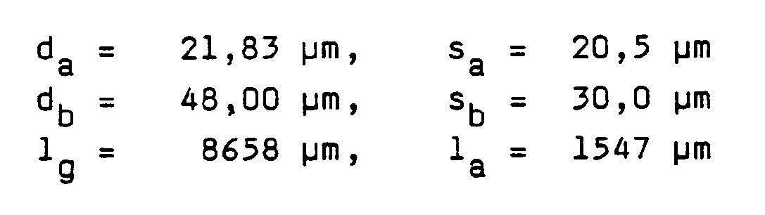
Für einen Schreibkopf mit 30 Heizelementen und einer Auflösung von 180 dots per inch (dpi) mit folgenden äußeren Abmessungen des Dünnfilmsubstrates DS, wie er in Figur 1 dargestellt ist, bzw. den vargegebenen Eingangsgrößen

ergeben sich unter Berücksichtigung des spezifischen Widerstandes dünner Aluminiumschichten ρAl= 3 · 10⁸ Ω m, wie sie für Leiterbahnen verwendet werden können und einer Leiterbahndicke h von 0,5 µm folgende, in der Tabelle 1 zusammengefaßten Werte für die Leiterbahnbreite dv, Spaltbreite sv und Länge der Übergangsstruktur 1v sowie der Gesamtwiderstand Rg

Taking into account the specific resistance of thin aluminum layers ρ Al = 3 · 10⁸ Ω m, as can be used for conductor tracks and a conductor track thickness h of 0.5 µm, the following values are summarized in Table 1 for the conductor track width d v , gap width s v and length of the
Als weiteres Beispiel diene ein Schreibkopf mit 300 dpi Auflösungsvermögen und 50 Heizelementen, dessen äußeren Abmessungen identisch den Abmessungen des oben beschriebenen Schreibkopfes (180 dpi) entsprechen.Another example is a print head with a resolution of 300 dpi and 50 heating elements, the external dimensions of which are identical to the dimensions of the print head described above (180 dpi).
Mit den Eingangsgrößen
- nmax
- = 50
- Al
- = 3 10⁻⁸ Ω m
- h
- = 0,5 µm
ergeben sich für

- n max
- = 50
- Al
- = 3 10⁻⁸ Ω m
- H
- = 0.5 µm
the values entered in Table 2 result for the 300 dpi print head.
Bei einer Spaltbreite sv = 20,5 µm beträgt damit der gesamte Zuleitungswiderstand pro Heizelement
beim 180 dpi Schreibkopf Rges = 2 · Rg = 15,2 Ω
und beim 300 dpi Schreibkopf Rges = 2 · Rg = 33,4 ΩWith a gap width s v = 20.5 µm, the total lead resistance per heating element is therefore
with the 180 dpi print head R tot = 2 · R g = 15.2 Ω
and with the 300 dpi print head R tot = 2 · R g = 33.4 Ω
In den Figuren 4 und 5 sind für eine angenommene Aluminiumdicke von h=0,5 die Gesamtzuleitungswiderstände Rges = 2 Rg als Funktionen der Leiterbahnbreite dv der Übergangsstruktur ÜV einmal für einen 180 dpi Schreibkopf (Fig.4) und einmal für einen 300 dpi Schreibkopf (Fig. 5) dargestellt.In FIGS. 4 and 5, for an assumed aluminum thickness of h = 0.5, the total lead resistances R tot = 2 R g as functions of the conductor width d v of the transition structure ÜV are once for a 180 dpi write head (FIG. 4) and once for a 300 dpi print head (Fig. 5) shown.
Claims (4)
- A method of optimizing a conductor path arrangement for a printer head in ink-jet printers in which a plurality of heating elements (RH) are selectively driven via conductor paths (Li) and these conductor paths (Li), distributed over a thin-film substrate (DS), lead to a Connection area (AF), wherein the conductor paths (Li) are fanned out into a closely spaced zone (LA) and a widely spaced zone (LB) and are connected by means of a transition structure (UV), characterised in that on the basis of the predetermined structural sizes of the two conductor path zones which are to be connected, namely the conductor path widths (da, db) and gap widths (Sa, Sb) and on the basis of the gap width (Sb) in the transition structure (UV), the conductor path width (dv) in the transition structure (UV) is dimensioned in accordance with the following equation


- A conductor path arrangement for a printer head in ink-jet printers in which a plurality of heating elements (RH) are selectively driven via conductor paths (Li) and these conductor paths (L₁), distributed over a thin-film substrate (DS), lead to a connection area (AF), wherein, commencing from the heating elements (RH) which are to be contacted, the conductor paths (Li) are fanned out into a zone (LA) which comprises closely spaced conductor paths, a zone (LB) which comprises widely spaced conductor paths and which is adjacent to the connection area (AF), and a transition structure (UV) which connects these two zones, characterised in that the widths (di) of the conductor paths (Li) and the intervals (gap widths si) between two adjacent conductor paths (L1, L2) within the respective zones (LA, LB, UV) are contrived to be constant and to differ in relation to the other zones (LA, LB, UV), that in dependence upon the conductor path widths (da, db) and the gap widths (sa, sb) of the conductor paths (Li) in the zones (LA, LB) and the gap width (Sv) in the transition zone (UV), the conductor path width (dv) in the transition structure (UV) is dimensioned such that all the conductor paths possess approximately the same supply line resistance (Rg).
- A conductor path arrangement as claimed in Claim 2, characterised in that the conductor paths (Li) extend in parallel to one another within the individual zones (LA, LB, LV).
- A conductor path arrangement as claimed in Claim 2, characterised in that the respective conductor paths of adjacent zones (LA, UV, LB) are arranged at right angles to one another.
Applications Claiming Priority (2)
| Application Number | Priority Date | Filing Date | Title |
|---|---|---|---|
| EP88120855 | 1988-12-14 | ||
| EP88120855 | 1988-12-14 |
Publications (2)
| Publication Number | Publication Date |
|---|---|
| EP0448614A1 EP0448614A1 (en) | 1991-10-02 |
| EP0448614B1 true EP0448614B1 (en) | 1993-06-09 |
Family
ID=8199661
Family Applications (1)
| Application Number | Title | Priority Date | Filing Date |
|---|---|---|---|
| EP19900900866 Expired - Lifetime EP0448614B1 (en) | 1988-12-14 | 1989-12-12 | Method of optimizing a conductor-path layout for the printing head of an ink printing device, and a conductor-path layout for such a printing head |
Country Status (4)
| Country | Link |
|---|---|
| EP (1) | EP0448614B1 (en) |
| JP (1) | JPH04506187A (en) |
| DE (1) | DE58904667D1 (en) |
| WO (1) | WO1990006853A1 (en) |
Families Citing this family (3)
| Publication number | Priority date | Publication date | Assignee | Title |
|---|---|---|---|---|
| DE4024545A1 (en) * | 1990-08-02 | 1992-02-06 | Boehringer Mannheim Gmbh | Metered delivery of biochemical analytical soln., esp. reagent |
| US6398347B1 (en) * | 2000-07-24 | 2002-06-04 | Hewlett-Packard Company | Energy balanced ink jet printhead |
| JP2021174849A (en) * | 2020-04-23 | 2021-11-01 | イビデン株式会社 | Wiring board |
Family Cites Families (1)
| Publication number | Priority date | Publication date | Assignee | Title |
|---|---|---|---|---|
| US4612554A (en) * | 1985-07-29 | 1986-09-16 | Xerox Corporation | High density thermal ink jet printhead |
-
1989
- 1989-12-12 DE DE9090900866T patent/DE58904667D1/en not_active Expired - Fee Related
- 1989-12-12 EP EP19900900866 patent/EP0448614B1/en not_active Expired - Lifetime
- 1989-12-12 JP JP2501461A patent/JPH04506187A/en active Pending
- 1989-12-12 WO PCT/EP1989/001526 patent/WO1990006853A1/en not_active Ceased
Also Published As
| Publication number | Publication date |
|---|---|
| DE58904667D1 (en) | 1993-07-15 |
| EP0448614A1 (en) | 1991-10-02 |
| JPH04506187A (en) | 1992-10-29 |
| WO1990006853A1 (en) | 1990-06-28 |
Similar Documents
| Publication | Publication Date | Title |
|---|---|---|
| DE68913012T2 (en) | Thermal color jet printer with multi-stage switching in the print head converters. | |
| DE69011647T2 (en) | Ink jet head, its manufacturing method, substrate for an ink jet head, control method therefor and ink jet device. | |
| DE3008487C2 (en) | ||
| DE60127761T2 (en) | Electrode structure of a display panel and method of making electrodes | |
| DE3610821C2 (en) | ||
| DE60131855T2 (en) | NARROW MULTICOLOR PRINT HEAD FOR INK JET PRINTING | |
| DE69408232T2 (en) | Self-aligning nozzle design for thermal inkjet printheads | |
| DE3536370C2 (en) | ||
| DE2840279C2 (en) | Inkjet printer | |
| DE4224345A1 (en) | THERMAL HEAD | |
| DE3027911A1 (en) | DOT WRITING HEAD FOR PRECISION PRINTERS AND METHOD FOR PRODUCING THE SAME | |
| DE69825324T2 (en) | THERMO HEAD AND THERMAL PRINTER | |
| EP0448614B1 (en) | Method of optimizing a conductor-path layout for the printing head of an ink printing device, and a conductor-path layout for such a printing head | |
| DE69514610T2 (en) | Structure of a drive plate for an ink ejection device | |
| DE69705132T2 (en) | Thermal inkjet printer and control method | |
| DE69512887T2 (en) | THERMAL PRINT HEAD WITH CONTROL CIRCUIT AND CONTROL ARRANGEMENT FOR THERMAL PRINT HEAD | |
| EP0177633B1 (en) | Electrothermal sheet recorder | |
| DE19709344A1 (en) | Printing process with array of narrow print segments | |
| DE2852353A1 (en) | ELECTROSTATIC PRINT HEAD | |
| DE69305398T2 (en) | Split thermal print head | |
| DE4201633C2 (en) | Thermal print head | |
| DE2852352C2 (en) | Electrostatic print head | |
| DE2810800C2 (en) | Multi-layer printed circuit | |
| DE69030054T2 (en) | Thermal head | |
| DE2809615A1 (en) | THERMAL PRESSURE DEVICE |
Legal Events
| Date | Code | Title | Description |
|---|---|---|---|
| PUAI | Public reference made under article 153(3) epc to a published international application that has entered the european phase |
Free format text: ORIGINAL CODE: 0009012 |
|
| 17P | Request for examination filed |
Effective date: 19910527 |
|
| AK | Designated contracting states |
Kind code of ref document: A1 Designated state(s): DE |
|
| 17Q | First examination report despatched |
Effective date: 19920622 |
|
| GRAA | (expected) grant |
Free format text: ORIGINAL CODE: 0009210 |
|
| AK | Designated contracting states |
Kind code of ref document: B1 Designated state(s): DE |
|
| REF | Corresponds to: |
Ref document number: 58904667 Country of ref document: DE Date of ref document: 19930715 |
|
| PGFP | Annual fee paid to national office [announced via postgrant information from national office to epo] |
Ref country code: DE Payment date: 19931227 Year of fee payment: 5 |
|
| PLBE | No opposition filed within time limit |
Free format text: ORIGINAL CODE: 0009261 |
|
| STAA | Information on the status of an ep patent application or granted ep patent |
Free format text: STATUS: NO OPPOSITION FILED WITHIN TIME LIMIT |
|
| 26N | No opposition filed | ||
| PG25 | Lapsed in a contracting state [announced via postgrant information from national office to epo] |
Ref country code: DE Effective date: 19950901 |