EP0451471A2 - Method and apparatus for polishing a semiconductor wafer - Google Patents
Method and apparatus for polishing a semiconductor wafer Download PDFInfo
- Publication number
- EP0451471A2 EP0451471A2 EP91102670A EP91102670A EP0451471A2 EP 0451471 A2 EP0451471 A2 EP 0451471A2 EP 91102670 A EP91102670 A EP 91102670A EP 91102670 A EP91102670 A EP 91102670A EP 0451471 A2 EP0451471 A2 EP 0451471A2
- Authority
- EP
- European Patent Office
- Prior art keywords
- carrier
- workpiece
- polishing
- wafer
- metal portion
- Prior art date
- Legal status (The legal status is an assumption and is not a legal conclusion. Google has not performed a legal analysis and makes no representation as to the accuracy of the status listed.)
- Withdrawn
Links
Images

Classifications
-
- B—PERFORMING OPERATIONS; TRANSPORTING
- B24—GRINDING; POLISHING
- B24B—MACHINES, DEVICES, OR PROCESSES FOR GRINDING OR POLISHING; DRESSING OR CONDITIONING OF ABRADING SURFACES; FEEDING OF GRINDING, POLISHING, OR LAPPING AGENTS
- B24B55/00—Safety devices for grinding or polishing machines; Accessories fitted to grinding or polishing machines for keeping tools or parts of the machine in good working condition
- B24B55/02—Equipment for cooling the grinding surfaces, e.g. devices for feeding coolant
-
- B—PERFORMING OPERATIONS; TRANSPORTING
- B24—GRINDING; POLISHING
- B24B—MACHINES, DEVICES, OR PROCESSES FOR GRINDING OR POLISHING; DRESSING OR CONDITIONING OF ABRADING SURFACES; FEEDING OF GRINDING, POLISHING, OR LAPPING AGENTS
- B24B37/00—Lapping machines or devices; Accessories
- B24B37/005—Control means for lapping machines or devices
- B24B37/015—Temperature control
-
- B—PERFORMING OPERATIONS; TRANSPORTING
- B24—GRINDING; POLISHING
- B24B—MACHINES, DEVICES, OR PROCESSES FOR GRINDING OR POLISHING; DRESSING OR CONDITIONING OF ABRADING SURFACES; FEEDING OF GRINDING, POLISHING, OR LAPPING AGENTS
- B24B37/00—Lapping machines or devices; Accessories
- B24B37/27—Work carriers
- B24B37/30—Work carriers for single side lapping of plane surfaces
Definitions
- This invention relates to a method and apparatus for polishing a semiconductor wafer, and, more particularly, to an improved method and apparatus so as to obtain a substantially uniform polishing action across the surface of the wafer.
- Various methods and tools for polishing a semiconductor wafer are known in the art.
- these tools include upper and lower plates, between which wafers are positioned for polishing.
- the two plates are moved relative to each other, and a slurry, consisting of an abrasive solution with or without an etching reagent, is fed between the plates to grind and flush away the material removed from the wafer.
- U.S. Pat. No. 4,313,284 issued to Walsh on Feb. 1982, discloses a method and apparatus for adjusting the surface shape of the upper plate or wafer carrier.
- a vacuum source is connected to the carrier, so as to apply a pressure difference which distorts the carrier into a concave shape.
- This shape is sought so that the carrier surface will conform to that of the lower plate or turntable (which mounts a polishing pad), which distorts from thermal and mechanical stress during polishing.
- both references the curvature of the wafer carrier surface is distorted so as to conform to the curvature of the turntable. Also, the distortion is obtained by changing the pressure applied to the wafer carrier.
- Neither reference seeks, however, to regulate the curvature of the wafer carrier surface, so that it is bowed with respect to the turntable, so as to produce a different degree of polishing action at different points across the wafer surface.
- the process involves polishing a surface on a semiconductor wafer by mounting the wafer to a wafer carrier comprising at least two materials having different coefficients of thermal expansion.
- the temperature of the carrier is regulated to control the radial curvature, thus imparting a convex (or concave) bias to the wafer.
- a greater polishing action can be effected at the center (or the edges) of the wafer, if desired, to achieve a uniform thickness of the surface being polished across the wafer.
- an improved apparatus for polishing a surface on a workpiece comprising a rotatable turntable assembly, a polishing pad supported on the assembly, a rotatable wafer carrier located above the assembly and adapted to hold a wafer during polishing, with the wafer positioned between the carrier and the polishing pad, and temperature regulating means, communicating with the carrier.
- the wafer carrier comprises at least two materials having different coefficients of thermal expansion. The temperature of the carrier is regulated via the temperature regulating means to control the radial curvature, to impart a concave or convex bias to a wafer mounted to the carrier during polishing.
- Fig. 1 shows an improved apparatus for polishing a semiconductor wafer 1.
- the apparatus includes a wafer carrier 2 which is coupled to a spindle 3, which in turn is coupled to any suitable motor or driving means (not shown) for moving the carrier 2 in the directions indicated by the arrows 4a, 4b and 4c (rotation).
- the spindle 3 supports a load 5, which is exerted against the carrier 2 and thus against the wafer 1 during polishing.
- the carrier 2 includes an edge portion 6, which prevents the wafer 1 from sliding out from under the carrier 2 as the carrier 2 moves.
- the turntable assembly 7 includes a polishing table 8, on which a polishing pad 9 is positioned, and the polishing table 8 is rotated around the shaft 10 in the direction indicated by the arrow 11 by any suitable motor or driving means (not shown).
- the wafer carrier 2 includes an upper portion 12 and a lower portion 13, the two portions 12 and 13 being made of materials having different coefficients of thermal expansion.
- the two portions 12 and 13 are made of any suitable materials, preferably metal, and are joined via a suitable brazing material 14, e.g. silver solder, known to those skilled in the art.
- the temperature of the wafer carrier 2 is regulated, and because the upper and lower portions 12 and 13 are made of materials having different coefficients of thermal expansion, a change is accordingly effected in the radial curvature of the carrier 2.
- the temperature of the carrier 2 is satisfactorily regulated by circulating a suitable fluid, such as water, through the carrier.
- the upper portion 12 is provided with a fluid chamber 15, in the form of a serpentine channel, located at the surface of the brazing material 14.
- a serpentine configuration is advantageous for uniformly regulating the temperature of the carrier 2.
- the fluid for heating/cooling the carrier 2 is introduced to and withdrawn from the chamber 15 via fluid inlet 16 and fluid outlet 17, respectively, within the interior of the spindle 3.
- the fluid flow path through the serpentine channel is best seen in Fig. 2.
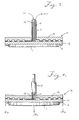
- the wafer carrier 2 is constructed so that it has a relatively flat shape, as shown in Fig. 3, at reference temperature, which is generally room temperature.
- reference temperature which is generally room temperature.
- the lower portion 13 is made of the material with the higher coefficient of thermal expansion, although this is not necessary.
- the temperature of the carrier is raised by increasing the temperature of the water flowing through the fluid chamber 15 above reference temperature, so as to cause the carrier to deflect upwardly at the outside edges, as depicted by the arrows 18a, 18b and 18c shown in Fig. 4. This results in an increase in polishing action at the center of the wafer, to compensate for the generally greater polishing action due to a higher slurry concentration at the wafer edges.
- the rate of polishing at the edges of the wafer 1 can be increased by cooling the carrier 2 below reference temperature. This will cause the carrier 2 to deflect downwardly at the outside edges to impart a concave bias to the wafer 2.
- the upper and lower portions, 12 and 13, respectively, of the carrier can be made of any suitable materials, so long as they have sufficiently different coefficients of thermal expansion for the degree of carrier deflection sought.
- the greater the difference in the relative coefficients of thermal expansion of the materials employed the greater the degree of deflection for a given temperature change.
- the more similar the coefficients are the less the degree of deflection for a given temperature change, and this may be particularly advantageous when more precise control is desired; if the coefficients are quite similar, for example, the degree of deflection may be quite small for a given temperature change.
- a stainless steel such as 304 stainless steel
- a nickel-based alloy such as "Hastelloy C” (available from Union Carbide Corp.), as the upper portion 12.
- the lower portion 13 can be made of the material with the lower coefficient of thermal expansion; this may be desirable, when it is desired to produce a concave deflection of the carrier 2 by effecting an increase in the carrier temperature. Under those circumstances, a decrease in carrier temperature, to below that of the reference temperature would, of course, produce, a convex deflection of the carrier 2.
- the method and apparatus of the invention allow wide lattitude in practice, to achieve a uniform polishing action over the wafer surface. Also, if desired, a dynamic adjustment can be made to achieve uniform radial polishing, by modulating the temperature of the carrier 2. This may be desired, for example, as a polish pad 9 becomes worn during use.
- the method and apparatus of the invention can be employed in polishing a wide variety of surface materials on the wafer, such as silicon, e.g. mono-crystalline silicon or polysilicon, common insulator materials, e.g. silicon dioxide, or other inorganic or organic insulator materials, e.g. polyimide, common conductor materials, e.g. metals, and so forth. Further, a surface which follows a varying topography can be polished, so that a uniform removal of material is achieved.
- silicon e.g. mono-crystalline silicon or polysilicon
- common insulator materials e.g. silicon dioxide
- other inorganic or organic insulator materials e.g. polyimide
- common conductor materials e.g. metals
Landscapes
- Engineering & Computer Science (AREA)
- Mechanical Engineering (AREA)
- Finish Polishing, Edge Sharpening, And Grinding By Specific Grinding Devices (AREA)
- Mechanical Treatment Of Semiconductor (AREA)
Abstract
Disclosed is an improved method of polishing a semiconductor wafer (1), which involves mounting the wafer (1) to a wafer carrier (2) comprising at least two materials (12, 13) having different coefficients of thermal expansion and regulating the temperature of the carrier (2), to thereby impart a convex (or concave) bias to the wafer (1). This provides an increased polishing action at the wafer center (or edges), so as to compensate for otherwise non-uniform radial polishing action across the wafer surface. Also disclosed, is an apparatus which incorporates the unique wafer carrier (2) and temperature regulating means for achieving the desired degree of radial curvature of the wafer carrier (2).
Description
- This invention relates to a method and apparatus for polishing a semiconductor wafer, and, more particularly, to an improved method and apparatus so as to obtain a substantially uniform polishing action across the surface of the wafer.
- Various methods and tools for polishing a semiconductor wafer are known in the art. In general, these tools include upper and lower plates, between which wafers are positioned for polishing. In operation, the two plates are moved relative to each other, and a slurry, consisting of an abrasive solution with or without an etching reagent, is fed between the plates to grind and flush away the material removed from the wafer.
- During polishing, it has been found, however, that the load imposed on the wafer leads to a higher concentration of slurry contacting the wafer edges, than its center. As a result, there is a greater polishing action at the edges, thus causing center-to-edge non-uniformity in thickness and poor flatness of the wafer.
- Efforts have been made in the art to obtain a more uniform polishing action across the wafer. For example, U.S. Pat. No. 4,313,284, issued to Walsh on Feb. 1982, discloses a method and apparatus for adjusting the surface shape of the upper plate or wafer carrier. In carrying out the method, a vacuum source is connected to the carrier, so as to apply a pressure difference which distorts the carrier into a concave shape. This shape is sought so that the carrier surface will conform to that of the lower plate or turntable (which mounts a polishing pad), which distorts from thermal and mechanical stress during polishing.
- Another approach is disclosed in U.S. Pat. No. 4,450,652, issued to Walsh on May 29, 1984, where a constant temperature is maintained on the top and bottom surfaces of the turntable to maintain the wafer carrier and the turntable at the same thermal bow distortion. The temperature differential is maintained constant by sensing the temperature of the polishing pad, then regulating the pressure applied to the wafer.
- In both references, the curvature of the wafer carrier surface is distorted so as to conform to the curvature of the turntable. Also, the distortion is obtained by changing the pressure applied to the wafer carrier. Neither reference seeks, however, to regulate the curvature of the wafer carrier surface, so that it is bowed with respect to the turntable, so as to produce a different degree of polishing action at different points across the wafer surface.
- Now, in accordance with the invention, an improved method of polishing a surface on a workpiece has been discovered. Preferably, the process involves polishing a surface on a semiconductor wafer by mounting the wafer to a wafer carrier comprising at least two materials having different coefficients of thermal expansion. The temperature of the carrier is regulated to control the radial curvature, thus imparting a convex (or concave) bias to the wafer. As a result, a greater polishing action can be effected at the center (or the edges) of the wafer, if desired, to achieve a uniform thickness of the surface being polished across the wafer.
- In accordance with another aspect of the invention, there is provided an improved apparatus for polishing a surface on a workpiece. In a preferred embodiment, the apparatus is used for polishing a surface on a semiconductor wafer, and it comprises a rotatable turntable assembly, a polishing pad supported on the assembly, a rotatable wafer carrier located above the assembly and adapted to hold a wafer during polishing, with the wafer positioned between the carrier and the polishing pad, and temperature regulating means, communicating with the carrier. It is a critical feature that the wafer carrier comprises at least two materials having different coefficients of thermal expansion. The temperature of the carrier is regulated via the temperature regulating means to control the radial curvature, to impart a concave or convex bias to a wafer mounted to the carrier during polishing.
- The foregoing and other objects, features and advantages of the invention will be apparent from the following more particular description of the preferred embodiments of the invention.
- Fig. 1
- is a schematic illustration , partially in cross-section, of an apparatus for polishing a semiconductor wafer, according to an embodiment of the invention;
- Fig. 2
- is a view in cross-section, somewhat enlarged, of the wafer carrier taken along the line 2-2 of Fig. 1;
- Fig. 3
- is a view in cross-section, with parts cut-away, of the wafer carrier taken along the line 3-3 of Fig. 2; and
- Fig. 4
- is a view in cross-section, similar to Fig. 3, of the wafer carrier, imparting a convex bias to a wafer.
- Referring to the drawings, Fig. 1 shows an improved apparatus for polishing a
semiconductor wafer 1. The apparatus includes awafer carrier 2 which is coupled to aspindle 3, which in turn is coupled to any suitable motor or driving means (not shown) for moving thecarrier 2 in the directions indicated by the arrows 4a, 4b and 4c (rotation). Thespindle 3 supports aload 5, which is exerted against thecarrier 2 and thus against thewafer 1 during polishing. Thecarrier 2 includes an edge portion 6, which prevents thewafer 1 from sliding out from under thecarrier 2 as thecarrier 2 moves. - The
semiconductor wafer 1, which is to be polished in accordance with the method of the invention, is shown mounted to thecarrier 2, positioned between the carrier and a rotatable turntable assembly, indicated generally by the numeral 7, located below thecarrier 2. The turntable assembly 7 includes a polishing table 8, on which a polishing pad 9 is positioned, and the polishing table 8 is rotated around the shaft 10 in the direction indicated by the arrow 11 by any suitable motor or driving means (not shown). - During polishing, a slurry (not shown) is usually applied between the
wafer carrier 2 and the polishing table 8. Due to theload 5 which is imposed on thewafer carrier 2, a higher concentration of slurry generally contacts the wafer edges, as previously noted, resulting in a greater polishing action at the edges. In order to overcome this problem, a unique wafer carrier structure is employed in accordance with the invention. Referring to Fig. 3, thewafer carrier 2 includes anupper portion 12 and alower portion 13, the twoportions portions - As described in more detail below, the temperature of the
wafer carrier 2 is regulated, and because the upper andlower portions carrier 2. The temperature of thecarrier 2 is satisfactorily regulated by circulating a suitable fluid, such as water, through the carrier. Theupper portion 12 is provided with a fluid chamber 15, in the form of a serpentine channel, located at the surface of the brazing material 14. A serpentine configuration is advantageous for uniformly regulating the temperature of thecarrier 2. The fluid for heating/cooling thecarrier 2 is introduced to and withdrawn from the chamber 15 viafluid inlet 16 andfluid outlet 17, respectively, within the interior of thespindle 3. The fluid flow path through the serpentine channel is best seen in Fig. 2. - In practice, the
wafer carrier 2 is constructed so that it has a relatively flat shape, as shown in Fig. 3, at reference temperature, which is generally room temperature. Generally, thelower portion 13 is made of the material with the higher coefficient of thermal expansion, although this is not necessary. Then, if it is desired to impart a convex bias to awafer 1 mounted to thecarrier 2, the temperature of the carrier is raised by increasing the temperature of the water flowing through the fluid chamber 15 above reference temperature, so as to cause the carrier to deflect upwardly at the outside edges, as depicted by the arrows 18a, 18b and 18c shown in Fig. 4. This results in an increase in polishing action at the center of the wafer, to compensate for the generally greater polishing action due to a higher slurry concentration at the wafer edges. - On the other hand, depending upon the particular apparatus being employed and the nature of the polishing action sought, the rate of polishing at the edges of the
wafer 1 can be increased by cooling thecarrier 2 below reference temperature. This will cause thecarrier 2 to deflect downwardly at the outside edges to impart a concave bias to thewafer 2. - The upper and lower portions, 12 and 13, respectively, of the carrier can be made of any suitable materials, so long as they have sufficiently different coefficients of thermal expansion for the degree of carrier deflection sought. As should be apparent, the greater the difference in the relative coefficients of thermal expansion of the materials employed, the greater the degree of deflection for a given temperature change. Conversely, the more similar the coefficients are, the less the degree of deflection for a given temperature change, and this may be particularly advantageous when more precise control is desired; if the coefficients are quite similar, for example, the degree of deflection may be quite small for a given temperature change. Although a wide selection of materials can be chosen, generally speaking, metals are preferred, and in one particularly preferred embodiment, a stainless steel, such as 304 stainless steel, is employed as the
lower portion 13, and a nickel-based alloy, such as "Hastelloy C" (available from Union Carbide Corp.), as theupper portion 12. - Various modifications can be made in the method and apparatus without departing from the spirit of the invention, as should be apparent to those skilled in the art. For example, the
lower portion 13 can be made of the material with the lower coefficient of thermal expansion; this may be desirable, when it is desired to produce a concave deflection of thecarrier 2 by effecting an increase in the carrier temperature. Under those circumstances, a decrease in carrier temperature, to below that of the reference temperature would, of course, produce, a convex deflection of thecarrier 2. - Thus, the method and apparatus of the invention allow wide lattitude in practice, to achieve a uniform polishing action over the wafer surface. Also, if desired, a dynamic adjustment can be made to achieve uniform radial polishing, by modulating the temperature of the
carrier 2. This may be desired, for example, as a polish pad 9 becomes worn during use. - In addition, the method and apparatus of the invention can be employed in polishing a wide variety of surface materials on the wafer, such as silicon, e.g. mono-crystalline silicon or polysilicon, common insulator materials, e.g. silicon dioxide, or other inorganic or organic insulator materials, e.g. polyimide, common conductor materials, e.g. metals, and so forth. Further, a surface which follows a varying topography can be polished, so that a uniform removal of material is achieved.
- As also should be apparent, a wide range of materials or workpieces, e.g. glass, can be polished. Moreover, it may be desired under some circumstances to form, instead of a uniformly flat surface, a surface having a degree of curvature, as desired. Other modifications should be apparent to those skilled in the art.
Claims (10)
- A method of polishing a surface on a workpiece, employing a polishing apparatus wherein said workpiece (1) is mounted to a carrier (2) and rotatably contacted with a plishing pad (9) to effect a polishing action across said workpiece (1), which method comprises mounting said workpiece (1) to a carrier (2) comprising at least two materials (12, 13) having different coefficients of thermal expansion, and regulating the temperature of said carrier (2) to control the radial curvature of said carrier, to impart a concave or convex bias to said workpiece (1) during polishing.
- The method of claim 1, wherein said carrier (2) comprises a lower metal portion (13) which mounts said workpiece (1) and an upper metal portion (12), said lower metal portion comprising said material having the higher coefficient of thermal expansion.
- The method of claim 2, wherein said lower metal portion (13) comprises a stainless steel and said upper metal portion (12) comprises a nickel-based alloy.
- The method of anyone of the claims 1 to 3, wherein the temperature of said carrier is regulated so as to impart a convex bias to said workpiece to increase the polishing action near the center of said workpiece (1) during polishing.
- The method of anyone of the claims 1 to 4, wherein said workpiece (1) is a semiconductor wafer.
- An apparatus for polishing a surface on a workpiece, comprising:
a rotatable turntable assembly (7);
a plishing pad (9) supported on said assembly;
a rotatable carrier (2), located above said assembly (7) and adapted to hold a workpiece (1) during polishing, with said workpiece (1) positioned between said carrier (2) and said plishing pad (9), said carrier (2) comprising at least two materials (12, 13) having different coefficients of thermal expansion; and
temperature regulating means (15, 16, 17) communicating with said carrier (2) for regulating the temperature of said carrier to control the radial curvature of said carrier, to impart a concave or convex bias to a workpiece (1) mounted to said carrier during polishing. - The apparatus of claim 6, wherein said temperature regulating means comprises a fluid chamber (15) within said carrier (2), and means (16, 17) for introducing and withdrawing fluid to and from said fluid chamber.
- The apparatus of claim 7, wherein said fluid chamber is a serpentine channel (15).
- The apparatus of anyone of the claims 6 to 8, wherein said carrier (2) comprises a lower metal portion (13) which is adapted to mount a workpiece (1) being polished and an upper metal portion (12), said lower portion (13) comprising said material having the higher coefficient of thermal expansion.
- The apparatus of claim 9, wherein said lower metal portion (13) comprises a stainless steel and said upper metal portion (12) comprises a nickel-based alloy.
Applications Claiming Priority (2)
| Application Number | Priority Date | Filing Date | Title |
|---|---|---|---|
| US509267 | 1990-04-13 | ||
| US07/509,267 US5036630A (en) | 1990-04-13 | 1990-04-13 | Radial uniformity control of semiconductor wafer polishing |
Publications (2)
| Publication Number | Publication Date |
|---|---|
| EP0451471A2 true EP0451471A2 (en) | 1991-10-16 |
| EP0451471A3 EP0451471A3 (en) | 1992-03-18 |
Family
ID=24025927
Family Applications (1)
| Application Number | Title | Priority Date | Filing Date |
|---|---|---|---|
| EP19910102670 Withdrawn EP0451471A3 (en) | 1990-04-13 | 1991-02-23 | Method and apparatus for polishing a semiconductor wafer |
Country Status (3)
| Country | Link |
|---|---|
| US (1) | US5036630A (en) |
| EP (1) | EP0451471A3 (en) |
| JP (1) | JPH078472B2 (en) |
Cited By (5)
| Publication number | Priority date | Publication date | Assignee | Title |
|---|---|---|---|---|
| EP0562718A1 (en) * | 1992-02-28 | 1993-09-29 | Shin-Etsu Handotai Company Limited | Polishing machine and method of dissipating heat therefrom |
| EP0598190A1 (en) * | 1992-09-18 | 1994-05-25 | Mitsubishi Materials Corporation | Apparatus for polishing wafer |
| WO1996024467A1 (en) * | 1995-02-10 | 1996-08-15 | Advanced Micro Devices, Inc. | Chemical-mechanical polishing using curved carriers |
| WO2001074534A3 (en) * | 2000-03-31 | 2002-02-07 | Speedfam Ipec Corp | A workpiece carrier with adjustable pressure zones and barriers |
| US7140956B1 (en) | 2000-03-31 | 2006-11-28 | Speedfam-Ipec Corporation | Work piece carrier with adjustable pressure zones and barriers and a method of planarizing a work piece |
Families Citing this family (69)
| Publication number | Priority date | Publication date | Assignee | Title |
|---|---|---|---|---|
| USRE36890E (en) * | 1990-07-31 | 2000-10-03 | Motorola, Inc. | Gradient chuck method for wafer bonding employing a convex pressure |
| US5527215A (en) * | 1992-01-10 | 1996-06-18 | Schlegel Corporation | Foam buffing pad having a finishing surface with a splash reducing configuration |
| JP3201833B2 (en) | 1992-07-27 | 2001-08-27 | 東芝機械株式会社 | Processing surface plate for polishing |
| US5302233A (en) * | 1993-03-19 | 1994-04-12 | Micron Semiconductor, Inc. | Method for shaping features of a semiconductor structure using chemical mechanical planarization (CMP) |
| US5435772A (en) * | 1993-04-30 | 1995-07-25 | Motorola, Inc. | Method of polishing a semiconductor substrate |
| US5329734A (en) * | 1993-04-30 | 1994-07-19 | Motorola, Inc. | Polishing pads used to chemical-mechanical polish a semiconductor substrate |
| US5700180A (en) | 1993-08-25 | 1997-12-23 | Micron Technology, Inc. | System for real-time control of semiconductor wafer polishing |
| US5658183A (en) * | 1993-08-25 | 1997-08-19 | Micron Technology, Inc. | System for real-time control of semiconductor wafer polishing including optical monitoring |
| US5584746A (en) * | 1993-10-18 | 1996-12-17 | Shin-Etsu Handotai Co., Ltd. | Method of polishing semiconductor wafers and apparatus therefor |
| JP3311116B2 (en) * | 1993-10-28 | 2002-08-05 | 株式会社東芝 | Semiconductor manufacturing equipment |
| US5441598A (en) * | 1993-12-16 | 1995-08-15 | Motorola, Inc. | Polishing pad for chemical-mechanical polishing of a semiconductor substrate |
| JP3042293B2 (en) * | 1994-02-18 | 2000-05-15 | 信越半導体株式会社 | Wafer polishing equipment |
| JPH07241764A (en) * | 1994-03-04 | 1995-09-19 | Fujitsu Ltd | Polishing device and polishing method |
| JP2914166B2 (en) * | 1994-03-16 | 1999-06-28 | 日本電気株式会社 | Polishing cloth surface treatment method and polishing apparatus |
| US5733175A (en) | 1994-04-25 | 1998-03-31 | Leach; Michael A. | Polishing a workpiece using equal velocity at all points overlapping a polisher |
| US5628869A (en) * | 1994-05-09 | 1997-05-13 | Lsi Logic Corporation | Plasma enhanced chemical vapor reactor with shaped electrodes |
| US5607341A (en) | 1994-08-08 | 1997-03-04 | Leach; Michael A. | Method and structure for polishing a wafer during manufacture of integrated circuits |
| JP3633062B2 (en) * | 1994-12-22 | 2005-03-30 | 株式会社デンソー | Polishing method and polishing apparatus |
| US5908530A (en) * | 1995-05-18 | 1999-06-01 | Obsidian, Inc. | Apparatus for chemical mechanical polishing |
| JPH09225819A (en) * | 1996-02-21 | 1997-09-02 | Shin Etsu Handotai Co Ltd | Holding mechanism for workpiece |
| USRE38854E1 (en) * | 1996-02-27 | 2005-10-25 | Ebara Corporation | Apparatus for and method for polishing workpiece |
| US5738568A (en) * | 1996-10-04 | 1998-04-14 | International Business Machines Corporation | Flexible tilted wafer carrier |
| US6056632A (en) * | 1997-02-13 | 2000-05-02 | Speedfam-Ipec Corp. | Semiconductor wafer polishing apparatus with a variable polishing force wafer carrier head |
| US5851140A (en) * | 1997-02-13 | 1998-12-22 | Integrated Process Equipment Corp. | Semiconductor wafer polishing apparatus with a flexible carrier plate |
| JPH10235552A (en) * | 1997-02-24 | 1998-09-08 | Ebara Corp | Polishing equipment |
| US6244946B1 (en) | 1997-04-08 | 2001-06-12 | Lam Research Corporation | Polishing head with removable subcarrier |
| US6425812B1 (en) | 1997-04-08 | 2002-07-30 | Lam Research Corporation | Polishing head for chemical mechanical polishing using linear planarization technology |
| US5885135A (en) * | 1997-04-23 | 1999-03-23 | International Business Machines Corporation | CMP wafer carrier for preferential polishing of a wafer |
| US6110025A (en) * | 1997-05-07 | 2000-08-29 | Obsidian, Inc. | Containment ring for substrate carrier apparatus |
| EP0881039B1 (en) * | 1997-05-28 | 2003-04-16 | Tokyo Seimitsu Co.,Ltd. | Wafer polishing apparatus with retainer ring |
| US5873769A (en) * | 1997-05-30 | 1999-02-23 | Industrial Technology Research Institute | Temperature compensated chemical mechanical polishing to achieve uniform removal rates |
| US6113479A (en) | 1997-07-25 | 2000-09-05 | Obsidian, Inc. | Wafer carrier for chemical mechanical planarization polishing |
| US6074288A (en) * | 1997-10-30 | 2000-06-13 | Lsi Logic Corporation | Modified carrier films to produce more uniformly polished substrate surfaces |
| DE19748020A1 (en) * | 1997-10-30 | 1999-05-06 | Wacker Siltronic Halbleitermat | Method and device for polishing semiconductor wafers |
| US6196896B1 (en) | 1997-10-31 | 2001-03-06 | Obsidian, Inc. | Chemical mechanical polisher |
| US5967885A (en) * | 1997-12-01 | 1999-10-19 | Lucent Technologies Inc. | Method of manufacturing an integrated circuit using chemical mechanical polishing |
| US6074286A (en) * | 1998-01-05 | 2000-06-13 | Micron Technology, Inc. | Wafer processing apparatus and method of processing a wafer utilizing a processing slurry |
| JP3693483B2 (en) * | 1998-01-30 | 2005-09-07 | 株式会社荏原製作所 | Polishing equipment |
| US5944588A (en) * | 1998-06-25 | 1999-08-31 | International Business Machines Corporation | Chemical mechanical polisher |
| US6012968A (en) * | 1998-07-31 | 2000-01-11 | International Business Machines Corporation | Apparatus for and method of conditioning chemical mechanical polishing pad during workpiece polishing cycle |
| US6129610A (en) * | 1998-08-14 | 2000-10-10 | International Business Machines Corporation | Polish pressure modulation in CMP to preferentially polish raised features |
| US6174221B1 (en) | 1998-09-01 | 2001-01-16 | Micron Technology, Inc. | Polishing chucks, semiconductor wafer polishing chucks, abrading methods, polishing methods, semiconductor wafer polishing methods, and methods of forming polishing chucks |
| JP3537688B2 (en) * | 1998-11-24 | 2004-06-14 | 富士通株式会社 | Processing method of magnetic head |
| US6491570B1 (en) | 1999-02-25 | 2002-12-10 | Applied Materials, Inc. | Polishing media stabilizer |
| US6066030A (en) * | 1999-03-04 | 2000-05-23 | International Business Machines Corporation | Electroetch and chemical mechanical polishing equipment |
| US6176764B1 (en) | 1999-03-10 | 2001-01-23 | Micron Technology, Inc. | Polishing chucks, semiconductor wafer polishing chucks, abrading methods, polishing methods, simiconductor wafer polishing methods, and methods of forming polishing chucks |
| US6077151A (en) * | 1999-05-17 | 2000-06-20 | Vlsi Technology, Inc. | Temperature control carrier head for chemical mechanical polishing process |
| US6325696B1 (en) | 1999-09-13 | 2001-12-04 | International Business Machines Corporation | Piezo-actuated CMP carrier |
| US6227939B1 (en) * | 2000-01-25 | 2001-05-08 | Agilent Technologies, Inc. | Temperature controlled chemical mechanical polishing method and apparatus |
| EP1602444B1 (en) * | 2000-01-31 | 2008-03-12 | Shin-Etsu Handotai Company Limited | Polishing method |
| KR100780099B1 (en) * | 2000-03-29 | 2007-11-29 | 신에쯔 한도타이 가부시키가이샤 | Work support base for polishing, polishing device and polishing method |
| US6666756B1 (en) | 2000-03-31 | 2003-12-23 | Lam Research Corporation | Wafer carrier head assembly |
| US6561884B1 (en) | 2000-08-29 | 2003-05-13 | Applied Materials, Inc. | Web lift system for chemical mechanical planarization |
| US6488565B1 (en) | 2000-08-29 | 2002-12-03 | Applied Materials, Inc. | Apparatus for chemical mechanical planarization having nested load cups |
| US6592439B1 (en) | 2000-11-10 | 2003-07-15 | Applied Materials, Inc. | Platen for retaining polishing material |
| US6503131B1 (en) | 2001-08-16 | 2003-01-07 | Applied Materials, Inc. | Integrated platen assembly for a chemical mechanical planarization system |
| KR100413493B1 (en) * | 2001-10-17 | 2004-01-03 | 주식회사 하이닉스반도체 | Polishing Platen of Chemical Mechanical Polishing Equipment and method for plating |
| US20070227901A1 (en) * | 2006-03-30 | 2007-10-04 | Applied Materials, Inc. | Temperature control for ECMP process |
| US8192248B2 (en) * | 2008-05-30 | 2012-06-05 | Memc Electronic Materials, Inc. | Semiconductor wafer polishing apparatus and method of polishing |
| CN102091994A (en) * | 2010-12-11 | 2011-06-15 | 昆明台兴精密机械有限责任公司 | Cooling device for spindle grinding disc of wafer single-side polishing machine |
| US10183376B1 (en) * | 2015-10-20 | 2019-01-22 | Seagate Technology Llc | Carrier for mounting a bar of sliders or a stack of such bars to be lapped |
| US10414018B2 (en) * | 2016-02-22 | 2019-09-17 | Ebara Corporation | Apparatus and method for regulating surface temperature of polishing pad |
| US11304290B2 (en) * | 2017-04-07 | 2022-04-12 | Taiwan Semiconductor Manufacturing Company, Ltd. | Semiconductor structures and methods |
| JP6893023B2 (en) * | 2017-06-08 | 2021-06-23 | スピードファム株式会社 | Polishing equipment |
| JP7201322B2 (en) * | 2018-01-05 | 2023-01-10 | 株式会社荏原製作所 | Polishing head for face-up polishing apparatus, polishing apparatus provided with the polishing head, and polishing method using the polishing apparatus |
| CN110744440A (en) * | 2019-10-22 | 2020-02-04 | 西安奕斯伟硅片技术有限公司 | A double-sided grinding device and method |
| JP7590131B2 (en) * | 2020-07-30 | 2024-11-26 | 株式会社東京精密 | Polishing Equipment |
| DE102020125246A1 (en) * | 2020-09-28 | 2022-03-31 | Lapmaster Wolters Gmbh | Double or single side processing machine |
| CN113043165A (en) * | 2021-03-16 | 2021-06-29 | 苏州赛万玉山智能科技有限公司 | Grinding and polishing structure, assembling method thereof and disassembling method of grinding tool or workpiece |
Family Cites Families (12)
| Publication number | Priority date | Publication date | Assignee | Title |
|---|---|---|---|---|
| DE2045515A1 (en) * | 1970-09-07 | 1972-03-09 | Burmah Oll Trading Ltd , London | Machine for lapping, polishing and the like |
| US4207381A (en) * | 1977-02-23 | 1980-06-10 | Tokyo Shibaura Electric Co., Ltd. | Bimetal and method for manufacturing the same |
| US4313284A (en) * | 1980-03-27 | 1982-02-02 | Monsanto Company | Apparatus for improving flatness of polished wafers |
| US4414286A (en) * | 1981-04-02 | 1983-11-08 | Texas Instruments Incorporated | Composite thermostat metal |
| DE3128880C2 (en) * | 1981-07-22 | 1987-03-19 | Fa. Peter Wolters, 2370 Rendsburg | Machine for lapping or polishing |
| US4450652A (en) * | 1981-09-04 | 1984-05-29 | Monsanto Company | Temperature control for wafer polishing |
| US4517041A (en) * | 1982-09-30 | 1985-05-14 | Magnetic Peripherals Inc. | Method for attaching a workpiece to a workpiece carrier |
| CH653369A5 (en) * | 1983-03-14 | 1985-12-31 | Bbc Brown Boveri & Cie | COMPOSITE MATERIAL IN BAR, TUBE, STRIP, SHEET OR PLATE SHAPE WITH REVERSIBLE THERMO-MECHANICAL PROPERTIES AND METHOD FOR THE PRODUCTION THEREOF. |
| JPS59187455A (en) * | 1983-04-05 | 1984-10-24 | Oki Electric Ind Co Ltd | Method of polishing insulating object separating base board |
| DE3604550A1 (en) * | 1986-02-13 | 1987-08-27 | Maho Ag | DEVICE FOR TEMPERATURE-DEPENDENT MEASURING POINT ADJUSTMENT OF TWO MACHINE PARTS |
| JPH0818571B2 (en) * | 1987-06-29 | 1996-02-28 | 日産自動車株式会社 | Power steering hydraulic control device |
| US4918869A (en) * | 1987-10-28 | 1990-04-24 | Fujikoshi Machinery Corporation | Method for lapping a wafer material and an apparatus therefor |
-
1990
- 1990-04-13 US US07/509,267 patent/US5036630A/en not_active Expired - Lifetime
-
1991
- 1991-02-23 EP EP19910102670 patent/EP0451471A3/en not_active Withdrawn
- 1991-03-07 JP JP3065357A patent/JPH078472B2/en not_active Expired - Lifetime
Cited By (10)
| Publication number | Priority date | Publication date | Assignee | Title |
|---|---|---|---|---|
| EP0562718A1 (en) * | 1992-02-28 | 1993-09-29 | Shin-Etsu Handotai Company Limited | Polishing machine and method of dissipating heat therefrom |
| US5718620A (en) * | 1992-02-28 | 1998-02-17 | Shin-Etsu Handotai | Polishing machine and method of dissipating heat therefrom |
| EP0598190A1 (en) * | 1992-09-18 | 1994-05-25 | Mitsubishi Materials Corporation | Apparatus for polishing wafer |
| US5618227A (en) * | 1992-09-18 | 1997-04-08 | Mitsubushi Materials Corporation | Apparatus for polishing wafer |
| WO1996024467A1 (en) * | 1995-02-10 | 1996-08-15 | Advanced Micro Devices, Inc. | Chemical-mechanical polishing using curved carriers |
| US5766058A (en) * | 1995-02-10 | 1998-06-16 | Advanced Micro Devices, Inc. | Chemical-mechanical polishing using curved carriers |
| WO2001074534A3 (en) * | 2000-03-31 | 2002-02-07 | Speedfam Ipec Corp | A workpiece carrier with adjustable pressure zones and barriers |
| US6612903B2 (en) | 2000-03-31 | 2003-09-02 | Speedfam-Ipec Corporation | Workpiece carrier with adjustable pressure zones and barriers |
| US6659850B2 (en) | 2000-03-31 | 2003-12-09 | Speedfam-Ipec Corporation | Work piece carrier with adjustable pressure zones and barriers and a method of planarizing a work piece |
| US7140956B1 (en) | 2000-03-31 | 2006-11-28 | Speedfam-Ipec Corporation | Work piece carrier with adjustable pressure zones and barriers and a method of planarizing a work piece |
Also Published As
| Publication number | Publication date |
|---|---|
| EP0451471A3 (en) | 1992-03-18 |
| JPH04217457A (en) | 1992-08-07 |
| US5036630A (en) | 1991-08-06 |
| JPH078472B2 (en) | 1995-02-01 |
Similar Documents
| Publication | Publication Date | Title |
|---|---|---|
| US5036630A (en) | Radial uniformity control of semiconductor wafer polishing | |
| KR840002114B1 (en) | Apparatus for improving flatness of polished wafers | |
| US5569062A (en) | Polishing pad conditioning | |
| US5558563A (en) | Method and apparatus for uniform polishing of a substrate | |
| US5868605A (en) | In-situ polishing pad flatness control | |
| US5888120A (en) | Method and apparatus for chemical mechanical polishing | |
| US5605499A (en) | Flattening method and flattening apparatus of a semiconductor device | |
| US6905400B2 (en) | Method and apparatus for dressing polishing cloth | |
| US3977130A (en) | Removal-compensating polishing apparatus | |
| KR100579431B1 (en) | Polishing method and polishing device | |
| JP2003224095A (en) | Chemical mechanical polishing equipment | |
| US6271140B1 (en) | Coaxial dressing for chemical mechanical polishing | |
| US5980685A (en) | Polishing apparatus | |
| US6991512B2 (en) | Apparatus for edge polishing uniformity control | |
| JPH09286021A (en) | Cutting method of semiconductor ingot | |
| JP2002542613A (en) | How to adjust a wafer polishing pad | |
| JP2636383B2 (en) | Wafer processing method | |
| JPH1058315A (en) | Polishing apparatus and polishing method | |
| JP2002166357A (en) | Wafer polishing method | |
| US6729945B2 (en) | Apparatus for controlling leading edge and trailing edge polishing | |
| US6878302B1 (en) | Method of polishing wafers | |
| US7033250B2 (en) | Method for chemical mechanical planarization | |
| JP3575944B2 (en) | Polishing method, polishing apparatus, and method of manufacturing semiconductor integrated circuit device | |
| JP3695842B2 (en) | Wafer polishing apparatus and wafer polishing method | |
| US20250353141A1 (en) | Method for dressing polishing pad, method for polishing silicon wafer, method for producing silicon wafer, and device for polishing silicon wafer |
Legal Events
| Date | Code | Title | Description |
|---|---|---|---|
| PUAI | Public reference made under article 153(3) epc to a published international application that has entered the european phase |
Free format text: ORIGINAL CODE: 0009012 |
|
| AK | Designated contracting states |
Kind code of ref document: A2 Designated state(s): DE FR GB |
|
| PUAL | Search report despatched |
Free format text: ORIGINAL CODE: 0009013 |
|
| 17P | Request for examination filed |
Effective date: 19911219 |
|
| AK | Designated contracting states |
Kind code of ref document: A3 Designated state(s): DE FR GB |
|
| STAA | Information on the status of an ep patent application or granted ep patent |
Free format text: STATUS: THE APPLICATION IS DEEMED TO BE WITHDRAWN |
|
| 18D | Application deemed to be withdrawn |
Effective date: 19930901 |