EP0455218B1 - Procédé et dispositif pour le mesurage d'un signal modulé en phase - Google Patents
Procédé et dispositif pour le mesurage d'un signal modulé en phase Download PDFInfo
- Publication number
- EP0455218B1 EP0455218B1 EP91107011A EP91107011A EP0455218B1 EP 0455218 B1 EP0455218 B1 EP 0455218B1 EP 91107011 A EP91107011 A EP 91107011A EP 91107011 A EP91107011 A EP 91107011A EP 0455218 B1 EP0455218 B1 EP 0455218B1
- Authority
- EP
- European Patent Office
- Prior art keywords
- phase
- steps
- calculated
- function
- carrier wave
- Prior art date
- Legal status (The legal status is an assumption and is not a legal conclusion. Google has not performed a legal analysis and makes no representation as to the accuracy of the status listed.)
- Expired - Lifetime
Links
Images


Classifications
-
- G—PHYSICS
- G01—MEASURING; TESTING
- G01J—MEASUREMENT OF INTENSITY, VELOCITY, SPECTRAL CONTENT, POLARISATION, PHASE OR PULSE CHARACTERISTICS OF INFRARED, VISIBLE OR ULTRAVIOLET LIGHT; COLORIMETRY; RADIATION PYROMETRY
- G01J9/00—Measuring optical phase difference; Determining degree of coherence; Measuring optical wavelength
- G01J9/02—Measuring optical phase difference; Determining degree of coherence; Measuring optical wavelength by interferometric methods
-
- G—PHYSICS
- G01—MEASURING; TESTING
- G01B—MEASURING LENGTH, THICKNESS OR SIMILAR LINEAR DIMENSIONS; MEASURING ANGLES; MEASURING AREAS; MEASURING IRREGULARITIES OF SURFACES OR CONTOURS
- G01B11/00—Measuring arrangements characterised by the use of optical techniques
- G01B11/24—Measuring arrangements characterised by the use of optical techniques for measuring contours or curvatures
- G01B11/2441—Measuring arrangements characterised by the use of optical techniques for measuring contours or curvatures using interferometry
-
- G—PHYSICS
- G01—MEASURING; TESTING
- G01B—MEASURING LENGTH, THICKNESS OR SIMILAR LINEAR DIMENSIONS; MEASURING ANGLES; MEASURING AREAS; MEASURING IRREGULARITIES OF SURFACES OR CONTOURS
- G01B11/00—Measuring arrangements characterised by the use of optical techniques
- G01B11/24—Measuring arrangements characterised by the use of optical techniques for measuring contours or curvatures
- G01B11/25—Measuring arrangements characterised by the use of optical techniques for measuring contours or curvatures by projecting a pattern, e.g. one or more lines, moiré fringes on the object
-
- G—PHYSICS
- G01—MEASURING; TESTING
- G01B—MEASURING LENGTH, THICKNESS OR SIMILAR LINEAR DIMENSIONS; MEASURING ANGLES; MEASURING AREAS; MEASURING IRREGULARITIES OF SURFACES OR CONTOURS
- G01B9/00—Measuring instruments characterised by the use of optical techniques
- G01B9/02—Interferometers
- G01B9/02015—Interferometers characterised by the beam path configuration
- G01B9/02032—Interferometers characterised by the beam path configuration generating a spatial carrier frequency, e.g. by creating lateral or angular offset between reference and object beam
-
- G—PHYSICS
- G01—MEASURING; TESTING
- G01B—MEASURING LENGTH, THICKNESS OR SIMILAR LINEAR DIMENSIONS; MEASURING ANGLES; MEASURING AREAS; MEASURING IRREGULARITIES OF SURFACES OR CONTOURS
- G01B9/00—Measuring instruments characterised by the use of optical techniques
- G01B9/02—Interferometers
- G01B9/02055—Reduction or prevention of errors; Testing; Calibration
- G01B9/02075—Reduction or prevention of errors; Testing; Calibration of particular errors
- G01B9/02078—Caused by ambiguity
- G01B9/02079—Quadrature detection, i.e. detecting relatively phase-shifted signals
- G01B9/02081—Quadrature detection, i.e. detecting relatively phase-shifted signals simultaneous quadrature detection, e.g. by spatial phase shifting
-
- G—PHYSICS
- G06—COMPUTING OR CALCULATING; COUNTING
- G06T—IMAGE DATA PROCESSING OR GENERATION, IN GENERAL
- G06T7/00—Image analysis
- G06T7/50—Depth or shape recovery
- G06T7/521—Depth or shape recovery from laser ranging, e.g. using interferometry; from the projection of structured light
-
- G—PHYSICS
- G01—MEASURING; TESTING
- G01J—MEASUREMENT OF INTENSITY, VELOCITY, SPECTRAL CONTENT, POLARISATION, PHASE OR PULSE CHARACTERISTICS OF INFRARED, VISIBLE OR ULTRAVIOLET LIGHT; COLORIMETRY; RADIATION PYROMETRY
- G01J9/00—Measuring optical phase difference; Determining degree of coherence; Measuring optical wavelength
- G01J9/02—Measuring optical phase difference; Determining degree of coherence; Measuring optical wavelength by interferometric methods
- G01J2009/0249—Measuring optical phase difference; Determining degree of coherence; Measuring optical wavelength by interferometric methods with modulation
Definitions
- the invention relates to a method for measuring the phase of a signal which is modulated on a carrier wave by phase modulation.
- the invention also relates to a device with which such a method can be carried out.
- phase measurement technology the signal is measured at several phase positions, with defined phase steps between the phase positions with respect to the carrier wave.
- the simplest known evaluation formula results if e.g. three measured values are recorded, which are at the phase positions ⁇ / 4, 3 ⁇ / 4 and 5 ⁇ / 4 with respect to the carrier wave.
- the total signal is measured with slightly changed phase positions, i.e. the phase positions with respect to the overall signal do not correspond to the desired phase positions with respect to the carrier wave.
- the consequence of this is that incorrect phase values of the modulation signal are measured systematically, so that the method only provides sufficiently accurate results if the frequency of the modulation signal is significantly lower than the frequency of the carrier wave.
- phase measurement technology is used in optical Measurement technology for the evaluation of strip images.
- an interferometer is known from US Pat. No. 4,744,659, the reference and measuring beams of which interfere with one another on a detector surface with predetermined angles of inclination. This inclination of the two beams creates a stripe pattern on the detector surface, which represents a spatial carrier wave. The frequency of this carrier wave is determined by the angle of inclination. Deviations of the surface profile of the measuring surface from the surface profile of the reference mirror lead to a spatial modulation of the stripe image, ie the phase position of the stripe image deviates locally from the phase position of the carrier wave determined by the angle of inclination.
- the intensity distribution of the stripe pattern is measured and the deviation of the phase position of the stripe pattern from the carrier wave determined by the angle of inclination is calculated by two-way Fourier transformation of the intensity distribution. For this purpose, a side band of the spatial frequency spectrum is filtered out by a window function.
- the two-way Fourier transformation means a relatively large amount of computation. An evaluation of the interferograms in video real time is therefore not possible.
- filtering out the sideband acts as a low-pass filter, which falsifies the measured values.
- the methods for evaluating multi-stripe interferograms only provide correct phase values if the stripe frequency of the stripe pattern matches the stripe frequency determined by the angle of inclination, i.e. if the profile of the measuring surface matches the profile of the reference surface. However, since the deviations of both profiles are to be measured, the measured values of interest are subject to a corresponding systematic error.
- phase shift interferometry is known, for example, from Applied Optics, 22, 3421, (1983).
- several interferograms are recorded one after the other without a spatial carrier wave.
- a temporal carrier wave is generated in that between the recording of the interferograms the reference mirror parallel to the optical axis (n-1) times around the same Distance ⁇ / 2n is shifted, where ⁇ is the wavelength of the light in the interferometer.
- This causes a phase shift of 2 ⁇ / n, where n is the number of interferograms.
- the invention is also intended to provide a device with which such a measuring method can be carried out with a reduced systematic error.
- the a i are chosen so that the phase error as a function of the phase shift has at least three zeros.
- the zeros can also degenerate into a single zero.
- the first and the second derivative of the error function have the value zero at the zero point. Determination equations for the a i result from the fact that the expressions match is required for several different phase levels.
- the phase error depending on the actual phase steps, has a profile which is proportional to sin 2 ⁇ with an amplitude ⁇ .
- the maximum amplitude ⁇ which results when, is designated as the error function of the phase value the actual phase levels differ from the target phase levels.
- the invention is based on the knowledge that the number of zeros of the error function can be chosen the greater the more sets of measured values are used in the linear combination.
- the signal is preferably measured at three different phase positions for each set of measured values. The number of measured values in each set is then minimal. Some of the measured values should also belong to several different sets of measured values at the same time. If the signal is then measured in total at m different phase positions, a formula can be used for the evaluation, the error function (m-2) of which has zeros.
- All measured values should preferably also be recorded in one period of the carrier wave.
- the measurement resolution is then high and the low-pass filtering is low.
- the method according to the invention is particularly suitable for evaluating stripe images, in particular multi-stripe images.
- the multi-stripe images can in particular be generated interferometrically or by recording a stripe pattern projected onto a test specimen. It enables the separate evaluation of individual multi-stripe images with high accuracy.
- the method can also be used advantageously in the multi-stripe interferometry mentioned at the beginning.
- the phase steps are then to be observed with less accuracy, while at the same time a high measuring accuracy is guaranteed.
- a hardware-based device for carrying out the method according to the invention provides at least 5 detectors which scan the signal at 5 different phase positions.
- the output signals of each detector are fed to two different amplification units, in which these output signals are each amplified by fixed factors and then accumulated in two different addition units.
- An evaluation unit calculates an associated phase value from the amplified and accumulated detector signals by forming the arc tangent of the quotient of the output signals of the two addition units.
- the operations described can also be carried out very quickly using modern digital electronics.
- the phase ⁇ is then calculated from the two quantities Z and N by tapping a tabulated function.
- the amplification factors of the two amplification units are selected for each detector such that the phase error as a function of the phase stages has at least three zeros. With such a device, a phase value can be calculated very precisely for each point of an optical stripe pattern.
- the detectors should then be optoelectronic sensors.
- the sensors are arranged in rows and columns on a surface.
- the number of rows and columns should be the same. It proves to be advantageous if the stripes of the stripe pattern lie diagonally to the rows and columns of the sensors, which improves the spatial resolution.
- two convolution components compute two expressions (Z, N) from a convolution of the brightness values of the image recorded by a camera, from which a phase value associated with a pixel is calculated.
- the convolution weights by which the brightness values are multiplied are chosen so that the phase error as a function of the phase shift has at least three zeros.
- the camera preferably has a CCD sensor, and the stripe pattern is preferably oriented diagonally to the columns and rows of the camera sensor.
- the task of phase measurement technology is to measure the phase value ⁇ as a function of the variable (P).
- the first case in which the variable (P) identifies the location, is particularly relevant when evaluating multi-stripe images.
- the second case, in which the variable (P) describes the time, relates in particular to phase shift interferometry, in which several interferograms recorded one after the other are evaluated.
- phase-modulated signal I (P) is now measured at five different phase positions, that is to say at five different values (P1 to P5) of the variables (P). The differences between these phase positions form the phase levels.
- the factors a1, a2, a3 are determined so that the phase error as a function of the phase steps has at least 3 zeros.
- phase modulated signal instead of five values of the variable P is generally measured at k values of the variable (P)
- the a i are chosen so that the phase error as a function of the phase steps (m-2) has zeros. Some of these zeros can also degenerate to higher order zeros.
- additional condition equations are set up, for example that are identical for certain phase levels.
- the phase-modulated signal (5) is measured at values (P1-P5) of the variables (P) which are shifted by 90 ° with respect to the carrier wave (4).
- the target phase levels are all identical here and amount to 90 °.
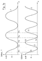
- Exemplary phase errors are plotted in FIG. 1b as a function of the phase steps if the actual phase steps deviate from the desired phase step.
- the phase error as a function of the phase steps between the measuring points has a profile which is proportional to sin (2 ⁇ ) with an amplitude ⁇ .
- the maximum amplitude ⁇ which results when the phase steps deviate from the desired phase steps, is plotted as an error function of the phase value.
- phase error 1b in FIG. 1b is the phase error that results when only 3 measuring points are used to calculate the phase value ⁇ .
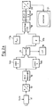
- the arrangement according to FIGS. 2a and 2b has a camera (11), which records a two-dimensional stripe pattern.
- the output signals of the camera (11) are digitized in an analog-digital converter and fed to an image memory (13).
- the image memory (13) only serves as a buffer memory. It can be dispensed with if the subsequent evaluation circuit is sufficiently fast.
- the digitized camera signals are fed to two convolution modules (14a, 14b).
- the folding module (14a) calculates a first expression (Z) by means of a two-dimensional folding operation and the second folding module (14b) also calculates a second expression (N) by means of a two-dimensional folding operation.
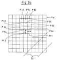
- FIG. 2b shows a section of 10x10 pixels of the camera sensor (11a) identified as squares.
- the recorded stripe pattern is indicated by the dashed lines (22). This stripe pattern lies diagonally to the rows and columns of the camera sensor (11a).
- An associated phase value is calculated for each pixel of the camera sensor (11a) by taking into account the intensity measurement values of the eight neighboring pixels.
- the intensity measurement values are thus folded within a convolution window of 3x3 points.
- the folding weights (Z ij ) and (N ij ) belonging to the points (Pij) of the folding window are listed in the following table: ij Z ij N ij P42 -2 -2 P52 3rd -1 P62 0 2nd P43 3rd -1 P53 0 4th P63 -3 -1 P44 0 2nd P54 -3 -1 P64 2nd -2
- folding weights (Z ij , N ij ) result in zeros of the error function for phase steps of 90 ° along the rows and columns of the camera pixels and for phase steps of 30 °, 90 ° and 150 ° along the direction perpendicular to the stripe pattern (22).
- the folding weights (Z ij ) are multiplied in the folding module (14a) by the intensity measurement values of the camera sensor at the respective point (Pij) and these nine folding products are then expressed added up.
- the folding weights (N ij ) in the folding module (14b) are multiplied by the intensity measurement values of the camera sensor at the respective point (P ij ) and then printed out added up.
- the expressions (Z, N) are assigned to that pixel which is in the middle of the convolution window, that is to say at the point designated (P53).
- the outputs of the two folding modules (14a, 14b) are fed to an arc tangent module (15) which calculates the arc tangent from the ratio Z / N of the two expressions (Z, N).
- the function values of the arctangent are stored in a look-up table (16).
- the phase values ⁇ calculated in this way are then stored in an image memory (17b) as a phase image.
- the entire camera image is scanned from the folding window. This is indicated in Fig. 2b by the two arrows (Pf1, Pf2).
- reference phase values which are stored in a further image memory (17a) are subtracted from the phase values of the image memory (17b).
- These reference phase values can be both mathematically calculated phase values that correspond to a target measurement result and the phase values of a calibration measurement.
- the difference between the phase values is temporarily stored in a further image memory (19), then analogized in a digital-to-analog converter (20) and displayed graphically on a monitor (21) used for data output.
- the orientation of the stripe pattern diagonally to the rows and columns of the camera sensor is particularly advantageous for two reasons: On the one hand, the error function has 3 zeros just perpendicular to the stripe direction, so that the phase values are determined with high accuracy even when the stripe frequency changes. Secondly, there is a distance between the measuring points perpendicular to the direction of the strip, which is 1 / ⁇ 2 smaller than the spacing of pixels of the camera sensor (11a), which are adjacent in rows and columns, which benefits the spatial resolution.
- the evaluation of the stripe pattern was explained with a convolution window that extends over 3x3 pixels of the camera sensor.
- the errors of the phase values can, however, still be significantly reduced if the intensity measurement values of a region of 5 ⁇ 5 pixels of the camera sensor are used for folding. In this case, the phase errors are significantly reduced, because the folding weights can then be selected so that the error function perpendicular to the strip direction and thus diagonally to the columns and rows of the camera sensor (11a) has seven zeros and three zeros in the direction of the rows and columns .
- the arrangement in Fig. 3 has nine light sensors (30a-30i), which are arranged square.
- the output signals of each light sensor (30a-i) are each fed to two amplifier groups (31a-i), (32a-i) which amplify the output signals of the light sensors (30a-i) by fixed factors.
- the output signals of the first amplifier group (31a-i) are accumulated in a first addition unit (33) to form an expression (Z) and the output signals of the second amplifier group (32a-i) are accumulated in a second addition unit to form a second expression (N).
- the arctangent is calculated from the ratio (Z / N) of the two expressions in an arc tangent module (35) from the two expressions (Z, N) and passed on for data output, which is indicated by the arrow (37).
- the function values of the arctangent are in turn stored in a lock-up table (36).
- the amplification factors of the two amplifier groups (31a-i), (32a-i) are selected analogously to the folding weights of a 3x3 folding window so that the error function of the phase value in one direction diagonal to the square of the light sensors (30a-i) has at least three zeros .
- Such a hard-wired sensor arrangement is particularly advantageous for the interferometer for distance measurement, which is shown in FIG. 4.
- the interferometer shown in FIG. 4 has a polarizing beam splitter (41) which directs the incident laser beam (40) into a measuring beam (42) and a reference beam (43). After passing through a ⁇ / 4 plate (44), the reference beam (43) is reflected on a reference mirror (45).
- the measuring beam (42) After passing through a second ⁇ / 4 plate (46), the measuring beam (42) is reflected on a reflecting surface (49) moving in the direction of the two arrows (47) and (48).
- the reflected measuring beam (42) and the reflected reference beam (43) are directed by the polarizing beam splitter (41) to a Wollaston prism (50).
- the Wollaston prism (50) causes the two partial beams to be inclined towards one another.
- a polarizer (51) is arranged behind the Wollaston prism, which makes the two inclined beams capable of interference.
- the inclination creates a stripe pattern that has the carrier frequency when the specular one Surface (49) is oriented perpendicular to the measuring beam (42).
- This stripe pattern is detected by a detector (52) according to FIG. 3.
- a shift of the reflecting surface (49) in the direction of the arrow (48) causes a change in the phase ( ⁇ ) determined by the detector (52).
- Tilting the reflecting surface (49) leads to a change in the carrier frequency.
- the phase value calculated by the detector (52) is largely independent of this carrier frequency, so that the phase value is also largely independent of a tilt of the reflecting surface (49).
Landscapes
- Physics & Mathematics (AREA)
- General Physics & Mathematics (AREA)
- Engineering & Computer Science (AREA)
- Computer Vision & Pattern Recognition (AREA)
- Spectroscopy & Molecular Physics (AREA)
- Optics & Photonics (AREA)
- Theoretical Computer Science (AREA)
- Length Measuring Devices By Optical Means (AREA)
- Measuring Phase Differences (AREA)
- Digital Transmission Methods That Use Modulated Carrier Waves (AREA)
Claims (12)
- Procédé pour le mesurage de la phase d'un signal qui est modulé sur une onde porteuse par une modulation de phase, dont les étapes consistent à:- relever des valeurs mesurées (I1 - I5) du signal pour plusieurs relations de phases (P1 - P5) qui sont séparées par des niveaux de phases intermédiaires, les niveaux de phases intermédiaires correspondant à des niveaux de phases théoriques par rapport à l'onde porteuse.- calculer la valeur de phase φ à partir du rapport (Z/N) d'une première expression Z et d'une deuxième expression N, la première expression Z et la deuxième expression N étant calculées à partir des valeurs mesurées (I1 - I5) et- où la première expression Z est formée de la combinaison linéaire

 - qu'au moins les trois expressions Zi d'un premier genre et en ce qu'au moins les trois expressions Ni d'un deuxième genre peuvent être calculées à partir des valeurs mesurées (I1 - I5) en considérant les niveaux de phases théoriques et en ce qu'elles sont choisies de sorte qu'à partir du rapport (Zi/Ni) de chaque expression du premier genre Zi et de l'expression associée d'un deuxième genre Ni pour un signal ayant la fréquence de l'onde porteuse, respectivement la même valeur correcte peut être calculée,- où, en cas d'écarts des niveaux de phases par rapport aux niveaux de phases théoriques, les valeurs de phase calculées sont entachées d'une erreur de phase qui présente un tracé périodique à valeur de phase double avec une amplitude désignée par ε comme fonction d'erreur de la valeur de phase et où- les facteurs ai sont choisis de sorte que la fonction d'erreur de la valeur de phase, comme fonction des niveaux de phases, a au moins trois zéros.
 - Procédé selon la revendication 1, caractérisé en ce que chacune des expressions Zi du premier genre et chacune des expressions Ni associées du deuxième genre est calculée au moyen des valeurs mesurées du signal pour trois relations de phases.
- Procédé selon la revendication 1, caractérisé en ce que les valeurs mesurées sont relevées durant une période de l'onde porteuse.
- Procédé selon l'une des revendications 1 - 3, caractérisé par son utilisation pour évaluer un photogramme.
- Procédé selon la revendication 4, caractérisé en ce que le photogramme est un multiphotogramme.
- Dispositif pour appliquer le procédé selon la revendication 1 pour le mesurage de la phase d'un signal qui est modulé sur une onde porteuse par une modulation de phase, avec des détecteurs (30a - i) mesurant le signal pour au moins cinq relations de phases différentes qui sont séparées par des niveaux de phases intermédiaires, les niveaux de phases intermédiaires correspondant aux niveaux de phases théoriques par rapport à l'onde porteuse, et avec une unité d'évaluation (35, 36) calculant une valeur de phase à partir de ces cinq valeurs mesurées, caractérisé en ce que- une première et une deuxième unité d'amplification (31a-i, 32a-i) sont prévues, vers lesquelles les signaux de sortie des détecteurs (30a-i) sont conduits,- une première unité d'addition (33) est prévue pour additionner les signaux de sortie de la première unité d'amplification (31a-i), associés aux relations de phases,- une deuxième unité d'addition (34) est prévue pour additionner les signaux de sortie de la deuxième unité d'amplification (32a-i), associés aux relations de phases,- et en ce que dans l'unité d'évaluation (35, 36) une valeur de phase associée est calculée à partir du quotient des signaux de détecteurs amplifiés et additionnés,- où, en cas d'écarts des niveaux de phases par rapport aux niveaux de phases théoriques, les valeurs de phase calculées sont entachées d'une erreur de phase qui présente un tracé périodique à valeur de phase double avec une amplitude désignée par ε comme fonction d'erreur de la valeur de phase et- où les facteurs d'amplification des deux unités d'amplification (31a-i, 32a-i) sont choisis en fonction des relations de phases respectives, de sorte que la fonction d'erreur de la valeur de phase, comme fonction des niveaux de phases, a au moins trois zéros.
- Dispositif selon la revendication 6, caractérisé en ce que les détecteurs (30a-i) sont des capteurs optoélectroniques.
- Dispositif selon la revendication 7, caractérisé en ce que les capteurs (30a-i) sont agencés sur une surface suivant des lignes et des colonnes et que le nombre de lignes et de colonnes est le même.
- Dispositif pour appliquer le procédé selon la revendication 1 pour le mesurage de la phase d'un signal qui est modulé sur une onde porteuse par une modulation de phase, avec des détecteurs (11) mesurant le signal pour au moins cinq relations de phases différentes qui sont espacées par des niveaux de phases intermédiaires, les niveaux de phases intermédiaires correspondant aux niveaux de phases théoriques par rapport à l'onde porteuse, avec deux modules (14a, 14b) de convolution branchés à la suite des détecteurs, qui calculent deux expressions (Z, N) par une convolution des signaux de détecteurs, à partir desquelles par la suite une valeur de phase associée est calculée en formant un quotient, caractérisé en ce que, dans les modules de convolution (14a, 14b), les signaux de détecteurs sont multipliés par des poids de convolution et les produits sont additionnés ensuite, qu'en cas d'écarts des niveaux de phases par rapport aux niveaux de phases théoriques, les valeurs de phases calculées sont entachées d'une erreur de phase qui présente un tracé périodique à valeur de phase double avec une amplitude désignée par ε comme fonction d'erreur de la valeur de phase et que les poids de convolution sont choisis de sorte que la fonction d'erreur de la valeur de phase, comme fonction des niveaux de phases, a au moins trois zéros.
- Dispositif selon la revendication 9, caractérisé en ce que les détecteurs sont des éléments de capteur d'une caméra (11).
- Dispositif selon la revendication 10, caractérisé par son utilisation pour le mesurage de la phase de bande d'une mire à bandes stationnaires.
- Dispositif selon la revendication 11, caractérisé en ce que la caméra (11) est une caméra avec dispositif à couplage de charge et que la mire à bandes est en diagonale par rapport aux colonnes et aux lignes du capteur de caméra.
Applications Claiming Priority (2)
| Application Number | Priority Date | Filing Date | Title |
|---|---|---|---|
| DE4014019 | 1990-05-02 | ||
| DE4014019A DE4014019A1 (de) | 1990-05-02 | 1990-05-02 | Verfahren zur messung eines phasenmodulierten signals |
Publications (2)
| Publication Number | Publication Date |
|---|---|
| EP0455218A1 EP0455218A1 (fr) | 1991-11-06 |
| EP0455218B1 true EP0455218B1 (fr) | 1995-01-11 |
Family
ID=6405537
Family Applications (1)
| Application Number | Title | Priority Date | Filing Date |
|---|---|---|---|
| EP91107011A Expired - Lifetime EP0455218B1 (fr) | 1990-05-02 | 1991-04-30 | Procédé et dispositif pour le mesurage d'un signal modulé en phase |
Country Status (5)
| Country | Link |
|---|---|
| US (1) | US5361312A (fr) |
| EP (1) | EP0455218B1 (fr) |
| JP (1) | JPH04230814A (fr) |
| CA (1) | CA2041621C (fr) |
| DE (2) | DE4014019A1 (fr) |
Cited By (3)
| Publication number | Priority date | Publication date | Assignee | Title |
|---|---|---|---|---|
| US7274467B2 (en) | 2005-01-04 | 2007-09-25 | Carl Zeiss Smt Ag | Phase shifting interferometric method, interferometer apparatus and method of manufacturing an optical element |
| DE102008006215A1 (de) | 2007-03-13 | 2008-09-18 | Carl Zeiss Smt Ag | Verfahren und Vorrichtung zum interferometrischen Vermessen einer Form einer optischen Fläche |
| US10962419B2 (en) | 2019-04-09 | 2021-03-30 | Carl Zeiss Optotechnik GmbH | Method for testing a tire by interferometry |
Families Citing this family (29)
| Publication number | Priority date | Publication date | Assignee | Title |
|---|---|---|---|---|
| US5268760A (en) * | 1991-06-07 | 1993-12-07 | Clarion Co., Ltd. | Motion adaptive impulse noise reduction circuit |
| DE4124223C2 (de) * | 1991-07-22 | 2001-07-26 | Zeiss Carl | Verfahren zur Auswertung von Interferogrammen und Interferometer |
| FR2685771A1 (fr) * | 1991-12-27 | 1993-07-02 | Bm Ind | Dispositif de mesure de la phase d'une onde lumineuse. |
| JPH09511078A (ja) * | 1993-12-12 | 1997-11-04 | エーエスピー ソルーション ユーエスエイ インコーポレイション | 信号処理方法および装置 |
| JP3338159B2 (ja) * | 1994-02-10 | 2002-10-28 | 三菱電機株式会社 | 振幅・位相検出装置 |
| US6804009B2 (en) * | 2000-05-03 | 2004-10-12 | The Regents Of The University Of California | Wollaston prism phase-stepping point diffraction interferometer and method |
| DE10301848B4 (de) * | 2003-01-09 | 2014-10-09 | Anton Rodi | Messeinrichtung zur Erfassung von Größen, insbesondere von Winkeln oder Wegstrecken |
| US7050175B1 (en) | 2003-08-08 | 2006-05-23 | Carl Zeiss Smt Ag | Method for calibrating an interferometer apparatus, for qualifying an optical surface, and for manufacturing a substrate having an optical surface |
| US7230717B2 (en) * | 2003-08-28 | 2007-06-12 | 4D Technology Corporation | Pixelated phase-mask interferometer |
| US7057737B2 (en) * | 2003-08-29 | 2006-06-06 | 4D Technology Corporation | Common optical-path testing of high-numerical-aperture wavefronts |
| US7342667B1 (en) | 2003-11-26 | 2008-03-11 | Carl Zeiss Smt Ag | Method of processing an optical element using an interferometer having an aspherical lens that transforms a first spherical beam type into a second spherical beam type |
| US7123365B1 (en) | 2004-03-05 | 2006-10-17 | Carl Zeiss Smt Ag | Method of calibrating an interferometer optics and method of processing an optical element having an aspherical surface |
| US20050225774A1 (en) * | 2004-04-05 | 2005-10-13 | Carl Zeiss Smt Ag | Method for measuring and manufacturing an optical element and optical apparatus |
| JP2007537426A (ja) * | 2004-05-14 | 2007-12-20 | カール・ツァイス・エスエムティー・アーゲー | 光学素子の製造方法 |
| US7061626B1 (en) | 2004-05-14 | 2006-06-13 | Carl Zeiss Smt Ag | Method of manufacturing an optical element using a hologram |
| US7167251B1 (en) | 2004-05-14 | 2007-01-23 | Carl Zeiss Smt Ag | Method of processing an optical substrate |
| US7436520B1 (en) | 2005-01-18 | 2008-10-14 | Carl Zeiss Smt Ag | Method of calibrating an interferometer optics and of processing an optical element having an optical surface |
| EP1842027A2 (fr) * | 2005-01-20 | 2007-10-10 | Carl Zeiss SMT AG | Hologramme et procede de fabrication d'un element optique mettant en oeuvre un hologramme |
| US20060274325A1 (en) * | 2005-05-23 | 2006-12-07 | Carl Zeiss Smt Ag | Method of qualifying a diffraction grating and method of manufacturing an optical element |
| DE102007046318A1 (de) * | 2007-09-27 | 2009-04-02 | Robert Bosch Gmbh | Abtastverfahren |
| US7619548B1 (en) * | 2008-06-20 | 2009-11-17 | Laser Technology, Inc. | Correlated noise and spurious signal reduction |
| DE102008030664A1 (de) | 2008-07-01 | 2010-01-21 | Carl Zeiss Smt Ag | Optische Abbildungseinrichtung mit Bestimmung von Abbildungsfehlern |
| US9103649B2 (en) | 2011-09-08 | 2015-08-11 | Zygo Corporation | In situ calibration of interferometers |
| DE102015209490A1 (de) | 2015-05-22 | 2016-11-24 | Carl Zeiss Smt Gmbh | Interferometrische Messanordnung |
| JPWO2017175341A1 (ja) * | 2016-04-06 | 2019-02-14 | 4Dセンサー株式会社 | 計測方法、計測装置、計測プログラム及び計測プログラムを記録した、コンピュータ読み取り可能な記録媒体 |
| CN112361992B (zh) * | 2020-11-10 | 2022-03-25 | 齐鲁工业大学 | 一种光栅投影三维测量方法及装置 |
| DE102021202909A1 (de) | 2021-03-25 | 2022-09-29 | Carl Zeiss Smt Gmbh | Messvorrichtung zum interferometrischen Vermessen einer Oberflächenform |
| DE102021004609A1 (de) | 2021-09-11 | 2023-03-16 | Eques Consulting GmbH | Vorrichtung und damit durchführbares Verfahren zur non-invasiven Konzentrationsbestimmung von Komponenten im menschlichen Blutkreislauf und Verwendung des Verfahrens. |
| CN118482666B (zh) * | 2024-07-16 | 2024-10-15 | 中国科学院光电技术研究所 | 一种用于可控空间载频移相干涉测量的调整装置及方法 |
Family Cites Families (7)
| Publication number | Priority date | Publication date | Assignee | Title |
|---|---|---|---|---|
| DE262080C (fr) * | ||||
| FR2510264A1 (fr) * | 1981-07-24 | 1983-01-28 | Thomson Csf | Dispositif de mesure de l'angle de phase entre un signal sinusoidal et un signal logique periodique de meme frequence |
| SU1256053A1 (ru) * | 1984-07-06 | 1986-09-07 | Ордена Ленина Институт Кибернетики Им.В.М.Глушкова | Знак дл маркировки деталей |
| US4744659A (en) * | 1985-03-20 | 1988-05-17 | Ricoh Company, Ltd. | Method of and apparatus for measuring the shape of a wavefront |
| SU1366966A1 (ru) * | 1986-03-24 | 1988-01-15 | Красноярский Политехнический Институт | Измеритель сдвига фаз |
| DE3707331A1 (de) * | 1987-03-07 | 1988-09-15 | Zeiss Carl Fa | Interferometer zur messung von optischen phasendifferenzen |
| DD262080A1 (de) * | 1987-07-08 | 1988-11-16 | Akad Wissenschaften Ddr | Verfahren und anordnung zur zeitaufgeloesten interferometrie |
-
1990
- 1990-05-02 DE DE4014019A patent/DE4014019A1/de not_active Withdrawn
-
1991
- 1991-04-30 DE DE59104197T patent/DE59104197D1/de not_active Expired - Fee Related
- 1991-04-30 EP EP91107011A patent/EP0455218B1/fr not_active Expired - Lifetime
- 1991-04-30 JP JP3098685A patent/JPH04230814A/ja active Pending
- 1991-05-01 CA CA002041621A patent/CA2041621C/fr not_active Expired - Fee Related
-
1993
- 1993-04-08 US US08/044,105 patent/US5361312A/en not_active Expired - Lifetime
Non-Patent Citations (3)
| Title |
|---|
| APPLIED OPTICS, vol. 24, no. 18, Y. Cheng et al.: "Phase shifter calibration in phase-shifting interferometry", 15.09.1985, Seiten 3049-3052 * |
| PROCEEDINGS OF THE SPIE, vol. 680, Katherine Creath: "Comparison of Phase Measurement Algorithms", USA, 1986 * |
| PROGRESS IN OPTICS, vol. XXVI, ed.: E. Wolf; Katherine Creath: "Phase-Measurement Interferometry Techniques", Elsevier Science Publishers B.V., Amsterdam, Oxford, New York, Tokyo, 1988 * |
Cited By (3)
| Publication number | Priority date | Publication date | Assignee | Title |
|---|---|---|---|---|
| US7274467B2 (en) | 2005-01-04 | 2007-09-25 | Carl Zeiss Smt Ag | Phase shifting interferometric method, interferometer apparatus and method of manufacturing an optical element |
| DE102008006215A1 (de) | 2007-03-13 | 2008-09-18 | Carl Zeiss Smt Ag | Verfahren und Vorrichtung zum interferometrischen Vermessen einer Form einer optischen Fläche |
| US10962419B2 (en) | 2019-04-09 | 2021-03-30 | Carl Zeiss Optotechnik GmbH | Method for testing a tire by interferometry |
Also Published As
| Publication number | Publication date |
|---|---|
| EP0455218A1 (fr) | 1991-11-06 |
| JPH04230814A (ja) | 1992-08-19 |
| US5361312A (en) | 1994-11-01 |
| CA2041621C (fr) | 2001-04-03 |
| DE59104197D1 (de) | 1995-02-23 |
| DE4014019A1 (de) | 1991-11-07 |
| CA2041621A1 (fr) | 1991-11-03 |
Similar Documents
| Publication | Publication Date | Title |
|---|---|---|
| EP0455218B1 (fr) | Procédé et dispositif pour le mesurage d'un signal modulé en phase | |
| DE3650220T2 (de) | Vorrichtung zur Abtastung einer optischen Wellenfront. | |
| EP0777853B1 (fr) | Dispositif de realisation de mesures spectroscopiques | |
| DE3306709C2 (fr) | ||
| DE2201830C3 (fr) | ||
| EP0670467B1 (fr) | Interféromètre | |
| DE69524298T2 (de) | Apparat und Verfahren zum Messen einer Verschiebung | |
| DE4204857C2 (de) | Verfahren zur Untersuchung einer Oberflächenform mit einem Interferometer | |
| EP0561015A1 (fr) | Mesure de phase interferométrique | |
| DE69313840T2 (de) | Photoelastische analyse mechanischer spannungen | |
| DE69033111T2 (de) | Apparat und Verfahren für die Ausmessung von dünnen mehrschichtigen Lagen | |
| DE69712872T2 (de) | Dreidimensionale farbbildaufnahme | |
| EP0449859B1 (fr) | Procede et dispositif d'observation de moirures sur des surfaces a examiner par moirage a dephasage | |
| DE3900247C2 (fr) | ||
| DE4013308A1 (de) | Verfahren zur optischen untersuchung von prueflingen | |
| DE19521295C2 (de) | Lichtelektrische Positionsmeßeinrichtung | |
| EP0626563B1 (fr) | Dispositif de mesure de positions avec l'échelle hologramme | |
| DE69627419T2 (de) | Fourier Spektrometer mit dichroitischen Michelson-Spiegeln für zwei Wellenlängenbänder | |
| DE4036120A1 (de) | Verfahren und vorrichtung zur bestimmung der wegaenderung von strahlen, vorzugsweise lichtstrahlen | |
| DE69406229T2 (de) | Optische Abbildungsvorrichtung für die Spektralanalyse einer Szene | |
| DE68918006T2 (de) | Deformationsmessverfahren und Vorrichtung mit Photoelementdetektoren. | |
| DE102019211665B4 (de) | Verfahren zur Ermittlung eines Gesamtspektrums einer Probe und Verfahren zur Aufnahme eines Gesamtspektrums einer Probe mittels eines Fourier-Transform-Spektrometers | |
| EP4124839A2 (fr) | Spectromètre spatial hétérodyne et procédé de mise en uvre d'une observation de la terre pousse-balai multidimensionnelle et multibande à haute résolution | |
| DE69634321T2 (de) | Optischer spektrumanalysator und spektroskop | |
| DD267787A1 (de) | Interferometrisches messsystem mit wellenlaengenkorrektureinrichtung des laserlichtes, insbesondere fuer laengenmessungen |
Legal Events
| Date | Code | Title | Description |
|---|---|---|---|
| PUAI | Public reference made under article 153(3) epc to a published international application that has entered the european phase |
Free format text: ORIGINAL CODE: 0009012 |
|
| AK | Designated contracting states |
Kind code of ref document: A1 Designated state(s): CH DE FR GB IT LI NL SE |
|
| 17P | Request for examination filed |
Effective date: 19920110 |
|
| 17Q | First examination report despatched |
Effective date: 19930428 |
|
| ITF | It: translation for a ep patent filed | ||
| GRAA | (expected) grant |
Free format text: ORIGINAL CODE: 0009210 |
|
| AK | Designated contracting states |
Kind code of ref document: B1 Designated state(s): CH DE FR GB IT LI NL SE |
|
| REF | Corresponds to: |
Ref document number: 59104197 Country of ref document: DE Date of ref document: 19950223 |
|
| PG25 | Lapsed in a contracting state [announced via postgrant information from national office to epo] |
Ref country code: SE Effective date: 19950411 |
|
| GBT | Gb: translation of ep patent filed (gb section 77(6)(a)/1977) |
Effective date: 19950315 |
|
| ET | Fr: translation filed | ||
| PLBE | No opposition filed within time limit |
Free format text: ORIGINAL CODE: 0009261 |
|
| STAA | Information on the status of an ep patent application or granted ep patent |
Free format text: STATUS: NO OPPOSITION FILED WITHIN TIME LIMIT |
|
| 26N | No opposition filed | ||
| REG | Reference to a national code |
Ref country code: GB Ref legal event code: IF02 |
|
| REG | Reference to a national code |
Ref country code: CH Ref legal event code: NV Representative=s name: LUCHS & PARTNER PATENTANWAELTE Ref country code: CH Ref legal event code: PUE Owner name: CARL ZEISS SMT AG Free format text: FIRMA CARL ZEISS#CARL-ZEISS-STRASSE 4-54 POSTFACH 1369/1380#D-73446 OBERKOCHEN (DE) -TRANSFER TO- CARL ZEISS SMT AG#CARL-ZEISS-STR. 22#73447 OBERKOCHEN (DE) |
|
| REG | Reference to a national code |
Ref country code: GB Ref legal event code: 732E |
|
| NLS | Nl: assignments of ep-patents |
Owner name: CARL ZEISS SMT AG |
|
| REG | Reference to a national code |
Ref country code: FR Ref legal event code: TP |
|
| PGFP | Annual fee paid to national office [announced via postgrant information from national office to epo] |
Ref country code: DE Payment date: 20080418 Year of fee payment: 18 Ref country code: CH Payment date: 20080415 Year of fee payment: 18 |
|
| PGFP | Annual fee paid to national office [announced via postgrant information from national office to epo] |
Ref country code: IT Payment date: 20080426 Year of fee payment: 18 |
|
| PGFP | Annual fee paid to national office [announced via postgrant information from national office to epo] |
Ref country code: NL Payment date: 20080415 Year of fee payment: 18 |
|
| PGFP | Annual fee paid to national office [announced via postgrant information from national office to epo] |
Ref country code: FR Payment date: 20080412 Year of fee payment: 18 |
|
| PGFP | Annual fee paid to national office [announced via postgrant information from national office to epo] |
Ref country code: GB Payment date: 20080421 Year of fee payment: 18 |
|
| REG | Reference to a national code |
Ref country code: CH Ref legal event code: PL |
|
| GBPC | Gb: european patent ceased through non-payment of renewal fee |
Effective date: 20090430 |
|
| NLV4 | Nl: lapsed or anulled due to non-payment of the annual fee |
Effective date: 20091101 |
|
| REG | Reference to a national code |
Ref country code: FR Ref legal event code: ST Effective date: 20091231 |
|
| PG25 | Lapsed in a contracting state [announced via postgrant information from national office to epo] |
Ref country code: CH Free format text: LAPSE BECAUSE OF NON-PAYMENT OF DUE FEES Effective date: 20090430 Ref country code: DE Free format text: LAPSE BECAUSE OF NON-PAYMENT OF DUE FEES Effective date: 20091103 Ref country code: LI Free format text: LAPSE BECAUSE OF NON-PAYMENT OF DUE FEES Effective date: 20090430 |
|
| PG25 | Lapsed in a contracting state [announced via postgrant information from national office to epo] |
Ref country code: NL Free format text: LAPSE BECAUSE OF NON-PAYMENT OF DUE FEES Effective date: 20091101 |
|
| PG25 | Lapsed in a contracting state [announced via postgrant information from national office to epo] |
Ref country code: GB Free format text: LAPSE BECAUSE OF NON-PAYMENT OF DUE FEES Effective date: 20090430 Ref country code: FR Free format text: LAPSE BECAUSE OF NON-PAYMENT OF DUE FEES Effective date: 20091222 |
|
| PG25 | Lapsed in a contracting state [announced via postgrant information from national office to epo] |
Ref country code: IT Free format text: LAPSE BECAUSE OF NON-PAYMENT OF DUE FEES Effective date: 20090430 |