EP0459979B1 - Procede de fabrication d'un reseau de fibres optiques - Google Patents
Procede de fabrication d'un reseau de fibres optiques Download PDFInfo
- Publication number
- EP0459979B1 EP0459979B1 EP89912087A EP89912087A EP0459979B1 EP 0459979 B1 EP0459979 B1 EP 0459979B1 EP 89912087 A EP89912087 A EP 89912087A EP 89912087 A EP89912087 A EP 89912087A EP 0459979 B1 EP0459979 B1 EP 0459979B1
- Authority
- EP
- European Patent Office
- Prior art keywords
- fibers
- grooves
- array
- fiber
- cladding
- Prior art date
- Legal status (The legal status is an assumption and is not a legal conclusion. Google has not performed a legal analysis and makes no representation as to the accuracy of the status listed.)
- Expired - Lifetime
Links
- 239000000835 fiber Substances 0.000 title claims abstract description 108
- 238000004519 manufacturing process Methods 0.000 title claims description 10
- 238000005253 cladding Methods 0.000 claims abstract description 24
- 239000013307 optical fiber Substances 0.000 claims abstract description 19
- 239000000758 substrate Substances 0.000 claims abstract description 19
- 238000000034 method Methods 0.000 claims abstract description 9
- 238000005530 etching Methods 0.000 claims description 15
- KRHYYFGTRYWZRS-UHFFFAOYSA-N Fluorane Chemical compound F KRHYYFGTRYWZRS-UHFFFAOYSA-N 0.000 claims description 8
- 230000009471 action Effects 0.000 claims description 5
- 239000002253 acid Substances 0.000 claims description 4
- 230000008569 process Effects 0.000 claims description 4
- 229910003460 diamond Inorganic materials 0.000 claims 1
- 239000010432 diamond Substances 0.000 claims 1
- 238000012856 packing Methods 0.000 abstract description 10
- 230000003287 optical effect Effects 0.000 abstract description 7
- 239000000853 adhesive Substances 0.000 description 9
- 230000001070 adhesive effect Effects 0.000 description 9
- 239000011521 glass Substances 0.000 description 9
- 239000004593 Epoxy Substances 0.000 description 6
- 238000004806 packaging method and process Methods 0.000 description 4
- 230000005855 radiation Effects 0.000 description 3
- CSCPPACGZOOCGX-UHFFFAOYSA-N Acetone Chemical compound CC(C)=O CSCPPACGZOOCGX-UHFFFAOYSA-N 0.000 description 2
- IJGRMHOSHXDMSA-UHFFFAOYSA-N Atomic nitrogen Chemical compound N#N IJGRMHOSHXDMSA-UHFFFAOYSA-N 0.000 description 2
- VYPSYNLAJGMNEJ-UHFFFAOYSA-N Silicium dioxide Chemical compound O=[Si]=O VYPSYNLAJGMNEJ-UHFFFAOYSA-N 0.000 description 2
- XUIMIQQOPSSXEZ-UHFFFAOYSA-N Silicon Chemical compound [Si] XUIMIQQOPSSXEZ-UHFFFAOYSA-N 0.000 description 2
- 238000003491 array Methods 0.000 description 2
- 238000005452 bending Methods 0.000 description 2
- 230000003139 buffering effect Effects 0.000 description 2
- 230000008878 coupling Effects 0.000 description 2
- 238000010168 coupling process Methods 0.000 description 2
- 238000005859 coupling reaction Methods 0.000 description 2
- QPJSUIGXIBEQAC-UHFFFAOYSA-N n-(2,4-dichloro-5-propan-2-yloxyphenyl)acetamide Chemical compound CC(C)OC1=CC(NC(C)=O)=C(Cl)C=C1Cl QPJSUIGXIBEQAC-UHFFFAOYSA-N 0.000 description 2
- 238000005498 polishing Methods 0.000 description 2
- 238000000926 separation method Methods 0.000 description 2
- 229910052710 silicon Inorganic materials 0.000 description 2
- 239000010703 silicon Substances 0.000 description 2
- KWYUFKZDYYNOTN-UHFFFAOYSA-M Potassium hydroxide Chemical compound [OH-].[K+] KWYUFKZDYYNOTN-UHFFFAOYSA-M 0.000 description 1
- 230000009286 beneficial effect Effects 0.000 description 1
- 230000008901 benefit Effects 0.000 description 1
- 230000005540 biological transmission Effects 0.000 description 1
- 239000004568 cement Substances 0.000 description 1
- 230000008859 change Effects 0.000 description 1
- 239000003795 chemical substances by application Substances 0.000 description 1
- 239000003086 colorant Substances 0.000 description 1
- 239000008367 deionised water Substances 0.000 description 1
- 229910021641 deionized water Inorganic materials 0.000 description 1
- 238000010586 diagram Methods 0.000 description 1
- 229910052732 germanium Inorganic materials 0.000 description 1
- GNPVGFCGXDBREM-UHFFFAOYSA-N germanium atom Chemical compound [Ge] GNPVGFCGXDBREM-UHFFFAOYSA-N 0.000 description 1
- 230000010365 information processing Effects 0.000 description 1
- 229910052757 nitrogen Inorganic materials 0.000 description 1
- 238000002360 preparation method Methods 0.000 description 1
- 230000000717 retained effect Effects 0.000 description 1
- 239000000377 silicon dioxide Substances 0.000 description 1
- 239000000126 substance Substances 0.000 description 1
- 239000011800 void material Substances 0.000 description 1
- XLYOFNOQVPJJNP-UHFFFAOYSA-N water Chemical compound O XLYOFNOQVPJJNP-UHFFFAOYSA-N 0.000 description 1
Images
Classifications
-
- G—PHYSICS
- G02—OPTICS
- G02B—OPTICAL ELEMENTS, SYSTEMS OR APPARATUS
- G02B26/00—Optical devices or arrangements for the control of light using movable or deformable optical elements
- G02B26/08—Optical devices or arrangements for the control of light using movable or deformable optical elements for controlling the direction of light
- G02B26/10—Scanning systems
- G02B26/103—Scanning systems having movable or deformable optical fibres, light guides or waveguides as scanning elements
-
- G—PHYSICS
- G02—OPTICS
- G02B—OPTICAL ELEMENTS, SYSTEMS OR APPARATUS
- G02B6/00—Light guides; Structural details of arrangements comprising light guides and other optical elements, e.g. couplings
- G02B6/24—Coupling light guides
- G02B6/245—Removing protective coverings of light guides before coupling
-
- G—PHYSICS
- G02—OPTICS
- G02B—OPTICAL ELEMENTS, SYSTEMS OR APPARATUS
- G02B6/00—Light guides; Structural details of arrangements comprising light guides and other optical elements, e.g. couplings
- G02B6/24—Coupling light guides
- G02B6/36—Mechanical coupling means
- G02B6/3628—Mechanical coupling means for mounting fibres to supporting carriers
- G02B6/3632—Mechanical coupling means for mounting fibres to supporting carriers characterised by the cross-sectional shape of the mechanical coupling means
- G02B6/3636—Mechanical coupling means for mounting fibres to supporting carriers characterised by the cross-sectional shape of the mechanical coupling means the mechanical coupling means being grooves
-
- G—PHYSICS
- G02—OPTICS
- G02B—OPTICAL ELEMENTS, SYSTEMS OR APPARATUS
- G02B6/00—Light guides; Structural details of arrangements comprising light guides and other optical elements, e.g. couplings
- G02B6/24—Coupling light guides
- G02B6/36—Mechanical coupling means
- G02B6/3628—Mechanical coupling means for mounting fibres to supporting carriers
- G02B6/368—Mechanical coupling means for mounting fibres to supporting carriers with pitch conversion between input and output plane, e.g. for increasing packing density
-
- G—PHYSICS
- G02—OPTICS
- G02B—OPTICAL ELEMENTS, SYSTEMS OR APPARATUS
- G02B6/00—Light guides; Structural details of arrangements comprising light guides and other optical elements, e.g. couplings
- G02B6/24—Coupling light guides
- G02B6/36—Mechanical coupling means
- G02B6/3628—Mechanical coupling means for mounting fibres to supporting carriers
- G02B6/3648—Supporting carriers of a microbench type, i.e. with micromachined additional mechanical structures
- G02B6/3652—Supporting carriers of a microbench type, i.e. with micromachined additional mechanical structures the additional structures being prepositioning mounting areas, allowing only movement in one dimension, e.g. grooves, trenches or vias in the microbench surface, i.e. self aligning supporting carriers
-
- G—PHYSICS
- G02—OPTICS
- G02B—OPTICAL ELEMENTS, SYSTEMS OR APPARATUS
- G02B6/00—Light guides; Structural details of arrangements comprising light guides and other optical elements, e.g. couplings
- G02B6/24—Coupling light guides
- G02B6/36—Mechanical coupling means
- G02B6/3628—Mechanical coupling means for mounting fibres to supporting carriers
- G02B6/3684—Mechanical coupling means for mounting fibres to supporting carriers characterised by the manufacturing process of surface profiling of the supporting carrier
- G02B6/3692—Mechanical coupling means for mounting fibres to supporting carriers characterised by the manufacturing process of surface profiling of the supporting carrier with surface micromachining involving etching, e.g. wet or dry etching steps
Definitions
- the present invention relates to a method of making a fiber optic array, and more particularly, to a method of making an array which has an increased packing density.
- optical fibers in a print head which is used to record information on a light-sensitive recording medium.
- the fibers can be arranged with their output ends in a linear array extending in a direction transverse to the direction of movement of the recording medium, and a light source, such as a light-emitting diode or a diode laser, can be connected to each of the fibers at an input end.
- the light in each of the fibers is modulated in accordance with an information signal to produce a desired image.
- Focusing means can be used in front of each fiber to cause the light to be focused to a point on the recording medium.
- the arrays of optical fibers prefferably have a high packing density, i.e., a high number of fibers per unit width of the array, in order to limit the amount of data buffering needed to produce the output image.
- a high packing density i.e., a high number of fibers per unit width of the array.
- an optical device for non-impact recording in which the recording head includes a linear array of optical fibers.
- the recording head comprises an adjustment plate having a plurality of grooves therein, and an optical fiber is secured in each of the grooves.
- the fibers have been arranged in grooves which converge toward the output end of the array to closely space the output ends of the fibers.
- one row of fibers is arranged above another row, and the fibers in the top row are offset relative to the fibers in the bottom row. In both of these embodiments, however, the packing density of the fibers is limited by the relatively large diameter of the fibers at their output ends.
- US-A-4,360,248 describes an optical star structure for combining and multiplexing optical signals. Said document states in the introductory portion relative to the prior art that "it has been proposed to increase the packing of fibers by thinning down the fiber claddings within the bundle adjacent the mixing section". However it also states that "this increase in the packing of fibers has been at the expense of higher light attenuation and losses in optical transmission efficiency.
- FP-A-2,500,642 describes a support having grooves to fix with respect to each other an index gradient lens and a bare optical fiber or an optical fiber with its jacket and its respective core.
- a principal advantage of the present invention is that a very high packing density of the fibers is obtained as a result of using fibers in which the cladding diameter at one end has been substantially reduced by etching.
- the array has a high packing density, there is no coupling of light between adjacent fibers. Since only an end portion of the fiber is etched, the strength and rigidity of the fiber is retained, and the fibers can be assembled in the array according to the method of the present invention without breakage. Outputs from the closely-spaced and independently-addressable fibers can be imaged onto a receiving medium through a single train of optics with diffraction-limited performance.
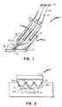
- Fiber optic array 10 constructed in accordance with the present invention.
- Fiber optic array 10 comprises three optical fibers 12 which are supported on a substrate 16.
- Each of the fibers 12 is connected by means of an optical fiber connector 18 to another optical fiber 20.
- Optical fiber connector 18 can be of the type shown in commonly-assigned U.S. Pat. No. 4,723,830, entitled Optical Fiber Connectors, issued Feb. 9, 1988.
- Each optical fiber 20 is connected to a light source 22, such as a diode laser or a light-emitting diode.
- Each light source 22 in array 10 can be modulated according to an information signal in a well-known manner.
- Array 10 can be used to record information on a light-sensitive medium (not shown) such as a photoconductor or photographic film.
- Array 10 can also be used as an optical scanner (not shown) in which light reflected from an object is transmitted through the optical fibers to photosensitive elements.
- each of the optical fibers 12 includes a jacket 30, a cladding 32, and a core 34.
- Jacket 30 has been removed from an end 31 of the fiber 12 to expose the cladding 32, and in a cladding portion 33 (Fig. 5), the diameter of the cladding is substantially reduced so that the portions 33 can be more closely spaced relative to each other.
- a tapered cladding portion 36 is formed at one end of portion 33.
- a fiber suitable for use in the present invention is a special single-mode fiber made by Corning Glass Works, Fiber No. 56704121,KH1. This fiber is made of silica with germanium doping in the core 34.
- the jacket 30 has a diameter of 250 »m
- the cladding 32 has a diameter of 125 »m
- the core 34 has a diameter of 4 »m.
- Other optical fibers can be used with the present invention, including multi-mode fibers.
- fibers 12 extend from an end 15 of array 10 which supports jackets 30 of the fibers to an opposite end 17 of the array, and the fibers 12 are closest together at the end 17.
- Fibers 12 are mounted in sets of grooves 28a and 28b which are formed in substrate 16, as shown in Fig. 3.
- the sets of grooves 28a and 28b are generally aligned, and the grooves in each set are generally parallel.
- a glass plate 21 extends over the fibers 12 in grooves 28b, and a similar plate (not shown) extends over the jackets 30 of fibers 12 in grooves 28b.
- These glass plates are very essential in the fabrication of array 10 as will be explained hereinafter.
- the glass plates 21 have been omitted in Fig. 1 in order to more clearly show elements of the present invention.
- an epoxy 23 which secures the fibers 12 in the grooves, fills the void areas between the plate 21, the substrate 16, and the fibers 12.
- Grooves 28a are sized to receive the jackets 30 of fibers 12. Grooves 28b are adapted to receive the cladding portions 33 of reduced diameter. As shown in Figs. 6A and 6B, the pitch p of the grooves 28a and 28b includes the width W of the grooves and the width S of lands 25a and 25b. The dimensions of the grooves 28a and 28b will depend on the size and type of fiber used in array 10.
- the pitch p of grooves 28a can be about 275 »m
- the pitch p of grooves 28b can be about 20 »m
- the width S of the land 25a can be about 25 »m
- the width S of land 25b can be about 4 »m.
- end 17 of array 16 is shown with portions 33 of a fibers 12 in grooves 28b.
- the dimensions of grooves 28b and portions 33 of fibers 12 are indicated in Fig. 2 where W is the maximum width of a groove 28b, ⁇ is the half angle of a groove 28f, S is the width of the land 25b, and P is the channel separation, that is the distance between the grooves 28b at bottoms 27b thereof.
- D is the diameter of cladding portion 33 of a fiber 12.
- the dimensions W, S, and P for various diameters D of portions 33 are shown in Table I.
- the angle ⁇ is about 35° for grooves etched in silicon; however, grooves of different angles can be used. TABLE I D(»m) W(»m) S(»m) P(»m) 10 12 4 16 20 24 4 28 30 36 4 40 40 49 4 53 50 61 4 65 100 146 4 150
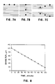
- a fiber 12 in which the jacket 30 has been removed from a portion thereof in preparation for an etching step.
- Fiber 12 is etched in hydrofluoric acid (HF) in order to reduce the diameter of cladding 32 from 125 »m to a diameter as small as 10 »m.
- HF hydrofluoric acid
- a plot of the etching characteristic is shown for room temperature. The nominal etching rate is 1.00 »m/min.
- the diameter of portion 33 must be large enough so there is no coupling of light between adjacent fibers. For best results, the diameter of the cladding in portion 33 should be at least 10 »m.
- the ends of fibers 12 are placed in the hydrofluoric acid, and the tapered portion 36 is formed above the surface of the HF acid as a result of capillary action. It has been found that the tapered portion 36 has a beneficial effect in that the bending strength of the fiber 12 is substantially greater than it would be if there were a sharp change from cladding 32 to the cladding portion 33 of reduced diameter.
- the core 34 of fiber 12 is etched faster than the cladding 34; as a result, a concave tip (not shown) is formed on core 34 which must be removed by polishing at a later stage in the process.
- the substrate 16 is preferably formed from a silicon wafer (not shown) by photolithographic means.
- a suitable mask (not shown) is used to form the grooves 28b for a plurality of substrates 16 on the wafer.
- the wafer is cleaned before and after etching using acetone and deionized water, and the wafer is then blown dry with nitrogen.
- the etching agent is a 12% potassium hydroxide (KOH) solution with a bath temperature of approximately 62°C. This results in an etching rate in groove depth of approximately 0.29 »m/min.
- Grooves 28a at end 15 of the substrate are formed last, and they are formed with a diamond-impregnated saw blade. Grooves 28a are adapted to receive the jackets 30 of the fibers 12.
- the grooves 28a are generally rectangular in cross section, and the width W is about 275 »m, the depth d is between about 60 and about 150 »m, and the width S of the lands 25a is about 25 »m.
- the jackets 30 of fibers 12 are first cemented in grooves 28a at end 15 of the array 10.
- the jackets 30 of fibers 12 are aligned in a holder (not shown), and the aligned fibers are then placed in grooves 28a on substrate 16.
- a glass plate e. g. a plate 21 as shown in Fig. 2, is placed over the jackets 30 in the grooves 28a.
- the glass plate can be about 150 »m thick and should be of a size to extend over the grooves 28a.
- the glass plate is held in place by a micropositioner, for example, a Model 221 micropositioner, obtainable from Rucker and Kolls.
- An ultraviolet light curable epoxy is introduced between the glass plate and substrate 16, and the epoxy is drawn into grooves 28a around the jackets 30 of fibers 12 by means of capillary action.
- the epoxy is cured by ultraviolet light.
- the portions 33 of fibers 12 are then eased into grooves 28b, and the portions 33 are cemented in place by means of a glass plate and a UV curable epoxy as described for jackets 30. That is, the glass plate is placed directly over the portions 33 and grooves 28b, the plate is held in position by a micropositioner, and UV curable epoxy is introduced around the fibers 12 in the grooves by means of capillary action.
- a portion of the array facet 19 is removed by means of a dicing saw, and in a final step, the facet is polished.
- the adhesive used to cement the fibers to the substrate.
- the adhesive must have low viscosity for good capillary action and a lower refractive index than that of the cladding to minimize radiation loss and cross talk between fibers. After the adhesive has cured, there should be low stress on the fiber to minimize micro-bending loss, and the adhesive should have adequate hardness to insure a polished surface of high quality.
- One suitable adhesive is Norland 61 adhesive which can be obtained from the Norland Co.
- a preferred adhesive is Lamdek U V Adhesive, Catalog No. 177 6921, obtainable from Dymax Engineering Adhesives, a division of American Chemical and Engineering Co., Torrington, CT.
- an array 10 was formed from single mode fibers having a core diameter of about 4 »m and a cladding diameter of about 125 »m.
- the portions 33 were etched to a diameter of about 15 »m, the length of portions 33 was about 25 mm after dicing and polishing, and the channel separation (P) between grooves 28b on substrate 16 was about 28 »m.
- the fibers 12 were mounted on a substrate 16 as shown in Fig. 1. The array thus formed was evaluated for taper/packaging loss, cross-talk level, and the output-beam quality.
- the taper/packaging loss is an indication of the radiation loss due to fiber taper, to the etched cladding, and to packaging stress in comparison to the radiation loss due to these factors from a free and normal single mode fiber. It was found that the propagation characteristics of the optical field were changed very little due to the etching and packaging in forming the array of the present invention, and thus, a substantial increase in packing density has been achieved in the array with practically no loss in the efficiency of the fibers.
- An array could extend the full length of a recording medium, or a recording head (not shown) could include a plurality of arrays arranged side-by-side or in parallel rows.
- An array 10 can also be used to produce various print formats, as shown in Fig. 7a-7c.
- the fibers 12 of array 10 are arranged to produce three spots in the line scan direction, each spot being separated by several pixels.
- the spots are aligned in the page scan direction, with each pixel separated by several lines
- Fig. 7c the spots are diagonally aligned and separated by variable spacings. Since the spots in Fig.
- an output device would include data buffering means in the information processing electronics, as is well-known in the art.
- the arrangement in Fig. 7a could be used, for example, in a color-recording device in which each of the spots represents one of the primary colors.
Landscapes
- Physics & Mathematics (AREA)
- General Physics & Mathematics (AREA)
- Optics & Photonics (AREA)
- Optical Couplings Of Light Guides (AREA)
- Light Guides In General And Applications Therefor (AREA)
- Printers Or Recording Devices Using Electromagnetic And Radiation Means (AREA)
- Mechanical Coupling Of Light Guides (AREA)
Abstract
Claims (5)
- Procédé de fabrication d'un réseau de fibres optiques, comprenant les étapes suivantes :a) la formation d'un premier ensemble de gorges dans un substrat (16), les gorges étant disposées jusqu'à une première extrémité (15) du substrat,b) la disposition de fibres (12) dans les gorges de manière que toutes les fibres soient disposées de manière générale dans la même direction,c) le collage des fibres dans les gorges,
caractérisé en ce qu'il comprend en outre :d) la formation d'un second ensemble de gorges (19) dans le substrat, les gorges étant disposées jusqu'à une seconde extrémité du substrat qui est opposée à la première extrémité, le pas du second ensemble de gorges étant inférieur au diamètre original des fibres,e) l'extraction radiale d'une partie du revêtement d'une extrémité de plusieurs fibres optiques pour la formation de fibres (33) dans lesquelles la première extrémité a un revêtement de dimension externe réduite par rapport à la dimension externe du revêtement à l'autre extrémité de la fibre, la dimension externe étant inférieure au pas du second ensemble de gorges,f) la disposition des extrémités réduites des fibres dans les gorges du second ensemble de gorges, etg) le collage des extrémités réduites dans les gorges. - Procédé de fabrication d'un réseau de fibres optiques selon la revendication 1, dans lequel le revêtement est retiré par attaque de la fibre dans l'acide fluorhydrique.
- Procédé de fabrication d'un réseau de fibres optiques selon la revendication 1 ou 2, dans lequel les gorges de certains des ensembles sont formées par des techniques photolithographiques.
- Procédé de fabrication d'un réseau de fibres optiques selon l'une quelconque des revendications 1 à 3, dans lequel les gorges de l'un des ensembles sont formées par une scie diamantée.
- Procédé de fabrication d'un réseau de fibres optiques selon l'une quelconque des revendications 1 à 4, dans lequel les extrémités des fibres sont plongées dans l'acide pendant une opération d'attaque, et une partie de la fibre placée au-dessus de l'acide est exposée à l'acide par effet capillaire afin qu'elle forme une partie effilée de revêtement entre les extrémités de la fibre.
Applications Claiming Priority (3)
| Application Number | Priority Date | Filing Date | Title |
|---|---|---|---|
| US254756 | 1988-10-07 | ||
| US07/254,756 US4875969A (en) | 1988-10-07 | 1988-10-07 | Method of making a fiber optic array |
| PCT/US1989/004244 WO1990004196A1 (fr) | 1988-10-07 | 1989-10-02 | Procede de fabrication d'un reseau de fibres optiques |
Publications (2)
| Publication Number | Publication Date |
|---|---|
| EP0459979A1 EP0459979A1 (fr) | 1991-12-11 |
| EP0459979B1 true EP0459979B1 (fr) | 1994-07-06 |
Family
ID=22965478
Family Applications (1)
| Application Number | Title | Priority Date | Filing Date |
|---|---|---|---|
| EP89912087A Expired - Lifetime EP0459979B1 (fr) | 1988-10-07 | 1989-10-02 | Procede de fabrication d'un reseau de fibres optiques |
Country Status (5)
| Country | Link |
|---|---|
| US (1) | US4875969A (fr) |
| EP (1) | EP0459979B1 (fr) |
| JP (1) | JP2801329B2 (fr) |
| DE (1) | DE68916653T2 (fr) |
| WO (1) | WO1990004196A1 (fr) |
Families Citing this family (28)
| Publication number | Priority date | Publication date | Assignee | Title |
|---|---|---|---|---|
| JP2718013B2 (ja) * | 1989-01-12 | 1998-02-25 | 住友電気工業株式会社 | 光ファイバ配線装置 |
| US5084828A (en) * | 1989-09-29 | 1992-01-28 | Healthtech Services Corp. | Interactive medication delivery system |
| US5006201A (en) * | 1989-11-22 | 1991-04-09 | Eastman Kodak Company | Method of making a fiber optic array |
| WO1992007716A1 (fr) | 1990-11-01 | 1992-05-14 | Landsman Robert M | Presse typographique |
| US5109460A (en) * | 1991-08-23 | 1992-04-28 | Eastman Kodak Company | Optical fiber array for a thermal printer and method of making same |
| US5379360A (en) * | 1992-06-03 | 1995-01-03 | Ngk Insulators, Ltd. | Optical fiber connector and method of manufacturing the same |
| FR2695384B1 (fr) * | 1992-09-04 | 1994-12-09 | Corning Inc | Procédé pour améliorer la fixation à l'aide d'un adhésif de fibres optiques à un substrat en verre, et composant optique intégré traité par ce procédé. |
| JPH06201936A (ja) * | 1992-12-28 | 1994-07-22 | Matsushita Electric Ind Co Ltd | 光ファイバアレイ及びその製造方法 |
| JP2851796B2 (ja) * | 1994-07-28 | 1999-01-27 | 日本碍子株式会社 | 光ファイバアレイの基板への固定方法 |
| JP3853866B2 (ja) * | 1995-02-21 | 2006-12-06 | 日本碍子株式会社 | 光ファイバー固定用基板 |
| JPH09120014A (ja) * | 1995-08-24 | 1997-05-06 | Ngk Insulators Ltd | 光ファイバアレイ |
| DE19607671B4 (de) * | 1996-02-29 | 2004-08-26 | INSTITUT FüR MIKROTECHNIK MAINZ GMBH | Verfahren zur Herstellung optischer Bauelemente mit angekoppelten Lichtwellenleitern und nach diesem Verfahren hergestellte Bauelemente |
| FR2749406B1 (fr) * | 1996-06-04 | 1998-08-07 | Laniepce Sylvie | Dispositif de transition de pas, notamment pour fibres optiques |
| JP3242360B2 (ja) * | 1997-03-17 | 2001-12-25 | ホーヤ株式会社 | 砥石、光ファイバガイドブロック製造用成形型の製造方法、光ファイバガイドブロック製造用成形型、および光ファイバガイドブロックの製造方法 |
| EP0980011A1 (fr) | 1998-08-13 | 2000-02-16 | Lucent Technologies Inc. | Fibre optique ayant une portion extrémale à section continûment décroissante et procédé pour sa fabrication |
| JP3931940B2 (ja) * | 1998-12-18 | 2007-06-20 | リコープリンティングシステムズ株式会社 | 光ファイバアレイ素子およびその製造方法 |
| JP4293733B2 (ja) | 1999-02-16 | 2009-07-08 | クウォンタム・コーポレイション | 磁気テープへのサーボ信号書き込み方法 |
| US6377739B1 (en) | 1999-03-09 | 2002-04-23 | Creo Srl | Two dimensional fiber optic output array |
| US6339470B1 (en) | 1999-04-26 | 2002-01-15 | Endovasix, Inc. | Apparatus and method for aligning an energy beam |
| JP2001343547A (ja) | 2000-03-30 | 2001-12-14 | Ngk Insulators Ltd | 光ファイバアレイ |
| JPWO2002023239A1 (ja) * | 2000-09-04 | 2004-01-22 | 日本碍子株式会社 | 光ファイバアレイ及びその製造方法 |
| FR2823859B1 (fr) * | 2001-04-19 | 2003-08-29 | Teem Photonics | Support de positionnement et de maintien de fibres optiques et son procede de realisation |
| US7080515B2 (en) | 2002-12-23 | 2006-07-25 | Siemens Westinghouse Power Corporation | Gas turbine can annular combustor |
| JP2005292718A (ja) * | 2004-04-05 | 2005-10-20 | Furukawa Electric Co Ltd:The | 光導波路、光導波路モジュールおよび光導波路の作成方法 |
| JP2009175505A (ja) * | 2008-01-25 | 2009-08-06 | Fujifilm Corp | 光ファイバ構造体 |
| CN102067194A (zh) * | 2008-07-02 | 2011-05-18 | 松下电器产业株式会社 | 引导装置 |
| CN111465879A (zh) * | 2017-10-26 | 2020-07-28 | 光研公司 | 导光装置、光波导装置、多波长光源模块及光波导装置的制造方法 |
| CN116047665A (zh) * | 2021-10-28 | 2023-05-02 | 武汉光迅科技股份有限公司 | 一种波长选择开关和电子设备 |
Citations (2)
| Publication number | Priority date | Publication date | Assignee | Title |
|---|---|---|---|---|
| FR2500642A1 (fr) * | 1981-02-24 | 1982-08-27 | Nippon Sheet Glass Co Ltd | Structure de support pour la fixation de fibres optiques et de lentilles et procede pour leur preparation ainsi que dispositif les utilisant |
| US4360248A (en) * | 1979-04-18 | 1982-11-23 | International Telephone And Telegraph Corporation | Multiport optical communication system and optical star structure therefor |
Family Cites Families (14)
| Publication number | Priority date | Publication date | Assignee | Title |
|---|---|---|---|---|
| US4165225A (en) * | 1975-04-17 | 1979-08-21 | Siemens Aktiengesellschaft | Distributor for optical signals |
| US4076378A (en) * | 1976-03-08 | 1978-02-28 | American Optical Corporation | Tapered fiber optic array |
| DE2938224A1 (de) * | 1979-09-21 | 1981-04-09 | Siemens AG, 1000 Berlin und 8000 München | Optische vorrichtung zum beruehrungslosen schreiben |
| DE2938301A1 (de) * | 1979-09-21 | 1981-04-09 | Siemens AG, 1000 Berlin und 8000 München | Optische vorrichtung zum beruehrungslosen schreiben, insbesondere zur faksimilewiedergabe von bildern und text |
| JPS5670505A (en) * | 1979-11-14 | 1981-06-12 | Fujitsu Ltd | Light branching filter circuit |
| DE3008106A1 (de) * | 1980-03-03 | 1981-09-10 | Siemens AG, 1000 Berlin und 8000 München | Vielfach-verzweigerelement |
| NL8103599A (nl) * | 1981-07-30 | 1983-02-16 | Philips Nv | Inrichting voor het optisch aftasten van een document. |
| US4556279A (en) * | 1981-11-09 | 1985-12-03 | Board Of Trustees Of The Leland Stanford Junior University | Passive fiber optic multiplexer |
| US4590492A (en) * | 1983-06-07 | 1986-05-20 | The United States Of America As Represented By The Secretary Of The Air Force | High resolution optical fiber print head |
| US4598975A (en) * | 1983-10-03 | 1986-07-08 | International Telephone And Telegraph Corporation | Multiple fiber linear array and method of making same |
| US4612028A (en) * | 1983-12-16 | 1986-09-16 | The United States Of America As Represented By The Secretary Of The Navy | Polarization-preserving single mode fiber coupler |
| US4723830A (en) * | 1984-06-22 | 1988-02-09 | Eastman Kodak Company | Optical fiber connectors |
| US4799949A (en) * | 1985-08-15 | 1989-01-24 | Corning Glass Works | Method of making low loss fiber optic coupler |
| JPS63147109A (ja) * | 1986-12-10 | 1988-06-20 | Nec Corp | 光フアイバ整列器 |
-
1988
- 1988-10-07 US US07/254,756 patent/US4875969A/en not_active Expired - Lifetime
-
1989
- 1989-10-02 DE DE68916653T patent/DE68916653T2/de not_active Expired - Fee Related
- 1989-10-02 WO PCT/US1989/004244 patent/WO1990004196A1/fr not_active Ceased
- 1989-10-02 EP EP89912087A patent/EP0459979B1/fr not_active Expired - Lifetime
- 1989-10-02 JP JP1511224A patent/JP2801329B2/ja not_active Expired - Lifetime
Patent Citations (2)
| Publication number | Priority date | Publication date | Assignee | Title |
|---|---|---|---|---|
| US4360248A (en) * | 1979-04-18 | 1982-11-23 | International Telephone And Telegraph Corporation | Multiport optical communication system and optical star structure therefor |
| FR2500642A1 (fr) * | 1981-02-24 | 1982-08-27 | Nippon Sheet Glass Co Ltd | Structure de support pour la fixation de fibres optiques et de lentilles et procede pour leur preparation ainsi que dispositif les utilisant |
Also Published As
| Publication number | Publication date |
|---|---|
| DE68916653T2 (de) | 1995-02-16 |
| JP2801329B2 (ja) | 1998-09-21 |
| JPH03504649A (ja) | 1991-10-09 |
| EP0459979A1 (fr) | 1991-12-11 |
| WO1990004196A1 (fr) | 1990-04-19 |
| US4875969A (en) | 1989-10-24 |
| DE68916653D1 (de) | 1994-08-11 |
Similar Documents
| Publication | Publication Date | Title |
|---|---|---|
| EP0459979B1 (fr) | Procede de fabrication d'un reseau de fibres optiques | |
| US4911526A (en) | Fiber optic array | |
| EP0393181B1 (fr) | Reseau de fibres optiques | |
| US4880494A (en) | Method of making a fiber optic array | |
| US5006201A (en) | Method of making a fiber optic array | |
| EP0534141B1 (fr) | Matrice de fibres optiques améliorée pour une imprimante thermique | |
| US4991930A (en) | Fiber optic array | |
| CA2291724A1 (fr) | Connecteur de groupement de fibres optiques de precision et procede | |
| EP0503707A1 (fr) | Méthode pour positioner et fixer des fibres optiques dans une rangée de fibres optiques et dispositif de couplage avec une telle rangée de fibres optiques | |
| JP2004101989A (ja) | 光ファイバアレイおよびそれを用いた光モジュール | |
| JP5337931B2 (ja) | 光ファイバアレイ | |
| JP4721672B2 (ja) | 光インターコネクト装置 | |
| JP2003255249A (ja) | 光記録装置用光ファイバアレイ及びそれを用いた画像形成装置 | |
| JPH1138270A (ja) | 光導波路ユニット | |
| JPH07120638A (ja) | 光接続素子およびその製造方法 | |
| JP2006126373A (ja) | 光波回路モジュールの光ファイバ用ガイド基板 | |
| JP3894262B2 (ja) | 光ファイバアレイ素子を用いた光走査装置 | |
| JPH0593878A (ja) | 多ビームによる光記録装置 | |
| JP4051565B2 (ja) | 光導波路型光記録装置の光導波路モジュール | |
| Haas et al. | Single-mode fiber printheads and scanline interleaving for high-resolution laser printing | |
| US20110123160A1 (en) | Dual floor densed fiber optic array | |
| RU2193788C1 (ru) | Волоконно-оптический кабель для многоканального акустооптического переключателя и способ его изготовления | |
| JP2001343601A (ja) | 光記録装置 | |
| JPH11271652A (ja) | マルチビームを用いた光記録装置 | |
| JP2003167165A (ja) | 光ファイバアレイ素子 |
Legal Events
| Date | Code | Title | Description |
|---|---|---|---|
| PUAI | Public reference made under article 153(3) epc to a published international application that has entered the european phase |
Free format text: ORIGINAL CODE: 0009012 |
|
| 17P | Request for examination filed |
Effective date: 19900925 |
|
| AK | Designated contracting states |
Kind code of ref document: A1 Designated state(s): DE FR GB |
|
| 17Q | First examination report despatched |
Effective date: 19921216 |
|
| GRAA | (expected) grant |
Free format text: ORIGINAL CODE: 0009210 |
|
| AK | Designated contracting states |
Kind code of ref document: B1 Designated state(s): DE FR GB |
|
| REF | Corresponds to: |
Ref document number: 68916653 Country of ref document: DE Date of ref document: 19940811 |
|
| ET | Fr: translation filed | ||
| PLBE | No opposition filed within time limit |
Free format text: ORIGINAL CODE: 0009261 |
|
| STAA | Information on the status of an ep patent application or granted ep patent |
Free format text: STATUS: NO OPPOSITION FILED WITHIN TIME LIMIT |
|
| 26N | No opposition filed | ||
| PGFP | Annual fee paid to national office [announced via postgrant information from national office to epo] |
Ref country code: GB Payment date: 20000918 Year of fee payment: 12 |
|
| PGFP | Annual fee paid to national office [announced via postgrant information from national office to epo] |
Ref country code: FR Payment date: 20001009 Year of fee payment: 12 |
|
| PGFP | Annual fee paid to national office [announced via postgrant information from national office to epo] |
Ref country code: DE Payment date: 20001030 Year of fee payment: 12 |
|
| PG25 | Lapsed in a contracting state [announced via postgrant information from national office to epo] |
Ref country code: GB Free format text: LAPSE BECAUSE OF NON-PAYMENT OF DUE FEES Effective date: 20011002 |
|
| REG | Reference to a national code |
Ref country code: GB Ref legal event code: IF02 |
|
| GBPC | Gb: european patent ceased through non-payment of renewal fee |
Effective date: 20011002 |
|
| PG25 | Lapsed in a contracting state [announced via postgrant information from national office to epo] |
Ref country code: FR Free format text: LAPSE BECAUSE OF NON-PAYMENT OF DUE FEES Effective date: 20020628 |
|
| PG25 | Lapsed in a contracting state [announced via postgrant information from national office to epo] |
Ref country code: DE Free format text: LAPSE BECAUSE OF NON-PAYMENT OF DUE FEES Effective date: 20020702 |
|
| REG | Reference to a national code |
Ref country code: FR Ref legal event code: ST |