EP0464180B1 - Bidirektionelle induktive datenübertragung mit vom meister betriebener unterstation - Google Patents
Bidirektionelle induktive datenübertragung mit vom meister betriebener unterstation Download PDFInfo
- Publication number
- EP0464180B1 EP0464180B1 EP91903008A EP91903008A EP0464180B1 EP 0464180 B1 EP0464180 B1 EP 0464180B1 EP 91903008 A EP91903008 A EP 91903008A EP 91903008 A EP91903008 A EP 91903008A EP 0464180 B1 EP0464180 B1 EP 0464180B1
- Authority
- EP
- European Patent Office
- Prior art keywords
- slave system
- circuit
- data
- impedance
- master
- Prior art date
- Legal status (The legal status is an assumption and is not a legal conclusion. Google has not performed a legal analysis and makes no representation as to the accuracy of the status listed.)
- Expired - Lifetime
Links
Images


Classifications
-
- A—HUMAN NECESSITIES
- A61—MEDICAL OR VETERINARY SCIENCE; HYGIENE
- A61N—ELECTROTHERAPY; MAGNETOTHERAPY; RADIATION THERAPY; ULTRASOUND THERAPY
- A61N1/00—Electrotherapy; Circuits therefor
- A61N1/18—Applying electric currents by contact electrodes
- A61N1/32—Applying electric currents by contact electrodes alternating or intermittent currents
- A61N1/36—Applying electric currents by contact electrodes alternating or intermittent currents for stimulation
- A61N1/372—Arrangements in connection with the implantation of stimulators
- A61N1/37211—Means for communicating with stimulators
- A61N1/37217—Means for communicating with stimulators characterised by the communication link, e.g. acoustic or tactile
- A61N1/37223—Circuits for electromagnetic coupling
-
- H—ELECTRICITY
- H04—ELECTRIC COMMUNICATION TECHNIQUE
- H04B—TRANSMISSION
- H04B5/00—Near-field transmission systems, e.g. inductive or capacitive transmission systems
- H04B5/20—Near-field transmission systems, e.g. inductive or capacitive transmission systems characterised by the transmission technique; characterised by the transmission medium
- H04B5/24—Inductive coupling
- H04B5/26—Inductive coupling using coils
- H04B5/266—One coil at each side, e.g. with primary and secondary coils
-
- H—ELECTRICITY
- H04—ELECTRIC COMMUNICATION TECHNIQUE
- H04B—TRANSMISSION
- H04B5/00—Near-field transmission systems, e.g. inductive or capacitive transmission systems
- H04B5/70—Near-field transmission systems, e.g. inductive or capacitive transmission systems specially adapted for specific purposes
-
- H—ELECTRICITY
- H04—ELECTRIC COMMUNICATION TECHNIQUE
- H04L—TRANSMISSION OF DIGITAL INFORMATION, e.g. TELEGRAPHIC COMMUNICATION
- H04L5/00—Arrangements affording multiple use of the transmission path
- H04L5/14—Two-way operation using the same type of signal, i.e. duplex
- H04L5/143—Two-way operation using the same type of signal, i.e. duplex for modulated signals
-
- A—HUMAN NECESSITIES
- A61—MEDICAL OR VETERINARY SCIENCE; HYGIENE
- A61N—ELECTROTHERAPY; MAGNETOTHERAPY; RADIATION THERAPY; ULTRASOUND THERAPY
- A61N1/00—Electrotherapy; Circuits therefor
- A61N1/18—Applying electric currents by contact electrodes
- A61N1/32—Applying electric currents by contact electrodes alternating or intermittent currents
- A61N1/36—Applying electric currents by contact electrodes alternating or intermittent currents for stimulation
- A61N1/372—Arrangements in connection with the implantation of stimulators
- A61N1/37211—Means for communicating with stimulators
- A61N1/37252—Details of algorithms or data aspects of communication system, e.g. handshaking, transmitting specific data or segmenting data
- A61N1/3727—Details of algorithms or data aspects of communication system, e.g. handshaking, transmitting specific data or segmenting data characterised by the modulation technique
-
- H—ELECTRICITY
- H04—ELECTRIC COMMUNICATION TECHNIQUE
- H04B—TRANSMISSION
- H04B5/00—Near-field transmission systems, e.g. inductive or capacitive transmission systems
- H04B5/70—Near-field transmission systems, e.g. inductive or capacitive transmission systems specially adapted for specific purposes
- H04B5/79—Near-field transmission systems, e.g. inductive or capacitive transmission systems specially adapted for specific purposes for data transfer in combination with power transfer
Definitions
- the invention relates to a device for the bidirectional transmission of information between a master system (transmitter) and a slave system (receiver) supplied electrically from the electromagnetic energy emitted by the master system.
- the slave system of which, devoid of any autonomous source of supply of electrical energy, is capable of receiving information, of electrically supplying electronic circuits or other charges, and to transmit information to the master system.
- slave system therefore designates a system comprising at least one antenna and reception circuits and which depends entirely on the “master system” for its supply of electrical energy, energy which is supplied to it in the form electromagnetic.
- Document GB-A-2 123 648 describes an implantable prosthesis for biological stimulation. comprising a reception antenna capable of picking up radiation carrying both control information and the energy necessary for the electrical supply of the circuits and charges of the prosthesis.
- the energy received is stored in a capacitor which, associated with a voltage regulator, is used to supply circuits for demodulating the received signal, for decoding the information conveyed by this signal, for controlling and supplying the stimulation electrodes, etc. ...
- the transmission of information takes place only from the transmitter to the receiver, so it is unidirectional.
- such a prosthesis or a similar implanted electronic device is also capable of transmitting measurement data to the outside on the electrical characteristics of the electrodes, on the operating state of its electrical circuits, data provided by sensors, etc.
- document WO 84/01719 describes a device for a similar application, the slave system of which is equipped with a transmitting antenna and circuits for transmitting said data.
- the slave system of this device therefore comprises both a receiver module and a transmitter module.
- the non-negligible energy necessary for the transmission of data by emission of electromagnetic radiation is added to the energy which the other circuits and loads consume which must supply the receiver module of the slave system.
- the instantaneous power extracted by the slave system from the radiation emitted by the master system is relatively low. In practice, this power proves to be insufficient to supply both the reception, control and transmission circuits and the electrical loads of the slave system.
- the device according to document US-A-4 741 340 and similar known devices do not make it possible to supply the slave system with electrical energy from the master system, and to ensure the transmission of a flow rate in a safe manner. high of information.
- the invention aims to provide a device allowing both the bidirectional transmission of high frequency information between a master system and a slave system and the electrical supply of the circuits and / or loads of the slave system from energy. electromagnetic emitted by the master system, and this with a single antenna both on the slave system side and on the master system side.
- the device according to the invention uses the electromagnetic coupling between the single transmitting antenna and the single receiving antenna to transmit information bidirectionally from the slave system to the master system, and this without electromagnetic radiation from the slave system, so that the essential to the electromagnetic energy received by the slave system is used to electrically supply the circuits and / or loads thereof.
- the energy necessary for the transmission of information from the slave system to the master system is essentially limited, at the level of the slave system, to the consumption of the electronic switch, for example a MOS transistor, which modulates the impedance of the slave system. This energy is therefore very low, and an appreciable fraction of the energy captured by the slave system remains available to supply its other circuits and loads, in particular those processing the data to be transmitted to the master system.
- the device according to the invention opens the way to numerous applications in which the use of an electric accumulator is excluded for the reasons mentioned above. If, for various reasons, an accumulator remains necessary, this device makes it possible to significantly improve the energy balance.
- the supply circuit comprises the combination of a series diode and a parallel capacitor.
- said detection means comprise means for detecting variations in the electric power consumed by said transmitting antenna.
- said detection means comprise means for detecting variations in the current / voltage phase shift in the transmitting antenna.
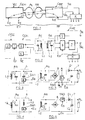
- the transmission device comprises a master system EM comprising a transmitting antenna A E and electrical transmission and processing circuits C EM connected to a power supply source (not shown ) which applies a voltage V cc to them .
- This master system EM has a data input E E and a data output S E.
- a slave system RE devoid of any connection with the master system EM, comprises a receiving antenna A R and electrical circuits for reception, supply and modulation C RE delivering on an output S R the data received from the master system EM and on a V AL output a continuous supply voltage.
- the RE slave system also includes a block K symbolizing electrical circuits such as, for example, circuits for processing the data delivered to the output S R , actuators, circuits for supplying electrodes or other loads, sensors collecting data which are applied to an input E R of the slave system RE in order to be transmitted to the master system EM under conditions which will be described below, etc.
- the two antennas A E and A R are LC type circuits tuned to the same carrier frequency f and coupled so that any modification of the electrical behavior of one of the systems has repercussions on the other system.
- the master system EM transmits on the frequency f which is modulated, for example in all or nothing, by the data applied to the input E E.
- the signal received by the receiving antenna A R from the transmitting antenna A E carries both this data and the energy necessary to supply the slave system RE.
- the electrical circuits C RE include conventional reception and supply circuits making it possible, on the one hand, to extract and format the data transmitted by the master system EM, the path of which is symbolized by the dashed line extending between the input E E and the output S R and, on the other hand, converting the energy received by the antenna A R into a continuous supply voltage V AL which supplies all the circuits on the side RE slave system.
- the transmission method which has just been described thus allows bidirectional transmission of information between the master system and the slave system on a single frequency, and this by means of a single antenna both on the master system side and on the slave system side. This therefore results in a saving of space both on the master system and the slave system, and a power saving at the level of the slave system because, as will emerge from the description which follows, the energy necessary to modulate the impedance of the slave system is extremely weak. This point is very important since the slave system only draws energy from the signal received from the master system and this energy must be used as a priority to supply a certain number of electrical loads such as actuators, sensors, different electronic circuits. , etc ... which are associated with the slave system.
- the reception and processing circuits C EM comprise a modulator 1 which modulates the signal at constant frequency delivered by a pilot oscillator 2, as a function of a modulation signal which is applied to it at entry E E.
- the modulation is preferably of the all or nothing type, that is to say that the signal from the pilot oscillator 2 is applied by the modulator 1 to the input of a power amplifier 3 (power required to supply the slave system) when the modulation signal is in a high state and no signal is applied to the input of the power amplifier 3 when the modulation signal is in the low state, or vice versa.
- the transmitting antenna A E is of the conventional type with inductance L1 and capacitance C1.
- the circuits C EM are supplemented by a circuit 4 for detecting or measuring the variations of an electrical characteristic induced in the master system EM by the modulation of the impedance of the slave system.
- the characteristic whose variations are detected can be a quantity representative of the module or of the argument of the impedance of the transmitting antenna A E.
- the antenna A R is also a tuned antenna of the type with inductance L2 and capacitor C2.
- the circuits C RE include conventional electronic reception circuits 5 which demodulate and format the signal received by the receiving antenna A R and deliver to the output S R the data transmitted by the master system EM.
- the antenna A R is also coupled to an impedance modulator circuit 6 which receives the data to be transmitted to the master system EM on its input E R.
- the circuits C RE are supplemented by a conventional supply circuit 7 which converts the energy received by the receiving antenna A R into a direct supply voltage V AL which is used to supply the various circuits or loads K connected to the slave system , in particular of the sensors applying data to the input E R of the modulation circuit 6.
- the impedance Z R of the slave system RE referred to the transmitting antenna A E is of the form R + j X where R represents the real part of this impedance and X its imaginary part.
- the real part R is essentially constituted by the losses due to the fact that the slave system consumes energy and has a certain equivalent resistance reduced to the master system.
- the imaginary part X is practically constant for a given carrier frequency and antenna tuning. To modulate the impedance Z R , it is therefore possible to vary its real part and / or its imaginary part.
- the diagram in FIG. 3 represents a first circuit associated with the receiving antenna A R to vary the imaginary part X of the impedance Z R.
- This first circuit comprises, in parallel with the inductance L2 and the capacitor C2, the series association of a capacitor C3 and an electronic switch SW1 controlled by the data applied to the input E R of the slave system.
- the switch SW1 when the switch SW1 is open, the impedance of the slave system RE is not affected, when this switch is closed the capacitor C3 is connected in parallel with the capacitor C2 and the imaginary part X of the impedance Z R is modified.
- the data applied to the control input E R of switch SW1 consists of a two-state signal, one of which requires the switch to close and the other to open.
- the modulation circuit 6 of FIG. 4 differs from that of FIG. 3 only in that the capacitor C3 is replaced by an inductance L3. As in the case of FIG. 3, switching on or off the inductance L3 has the effect of modifying the imaginary part of the impedance Z R.
- the circuits of FIGS. 3 and 4 offer the possibility of greatly varying the imaginary part X of the impedance Z R and thus of facilitating the measurement of the variations of the impedance Z E of the transmitting antenna.
- the switch SW1 for example a transistor, must be able to switch an alternating signal, have a very low stray capacitance and be able to withstand high voltages of the order of, for example 100 volts, since it is Frequently necessary to have such high voltages to ensure the operation of loads or electronic circuits associated with the slave system.
- FIGS. 5 and 6 Another possibility illustrated by FIGS. 5 and 6 consists in varying the real part R of the impedance Z R.
- the antenna A R is connected to the supply circuit 7 via a conventional rectifier bridge 8.
- the circuit 7 supplies all of the electronic circuits, sensors and other organs consuming electrical energy (block K) symbolized by a load R L in the figure.
- This circuit 7 conventionally consists of a diode D1 arranged in series in one of the output branches of the rectifier bridge 8 and of a storage capacitor C4 connected, between the output branches of the bridge, downstream of the diode D1 .
- An electronic switch SW2 is also connected between the output branches of the rectifier bridge 8, between the latter and the diode D1.
- the control electrode of the switch SW2 constitutes the input E R to which the data to be transmitted to the master system EM are applied.
- the modulation carried out by means of the switch SW2 has the effect of acting on the continuous consumption of the slave system.
- the modulation circuit has the advantage of being simple because it only switches DC voltages having a reference with respect to ground (O volt).
- the switch SW2 is closed, the impedance seen between its terminals A and B is weak.
- the diode D1 prevents the capacitor C4 from fully discharging through the switch SW2.
- the capacitor C4 which had been slightly discharged in the load R L , is recharged with a low impedance. Consequently, the real part R of the impedance Z R varies only slightly, especially in transient conditions, and the detection of the variations induced on the master system side is relatively difficult to ensure.
- FIG. 6 gives more satisfaction.
- This circuit differs from that of FIG. 5 in that the switch SW3 is connected, not between the output branches of the rectifier bridge 8, but in series between one of the output branches of the rectifier bridge 8 and the anode of diode D1, the other branch of the divider bridge being the one which is connected to ground.
- the control electrode of the switch SW3 constitutes the data input E R of the slave system.
- the real part R of the impedance Z R represents the losses in the antenna A R and R is then high.
- the switch SW3 is closed the real part R is represented by the paralleling of the ohmic losses in the antenna with the load R L representing the set of energy consuming elements. The real part R is then small, it is further reduced during the transient periods during which the capacitor C4 must recharge.
- the circuit of FIG. 6 therefore makes it possible to induce significant variations in the real part R of the impedance Z R and thus to easily detect the variations induced on the impedance Z E of the transmitting antenna A E.
- the electronic switch SW3 is referenced with respect to the output voltage of the rectifier, which leads to the use of a PNP transistor or PMOS more difficult to control than in the case of FIG. 5.
- FIG. 7 shows a particular embodiment of the switch SW3 of FIG. 6.
- This switch comprises a PNP transistor T1 whose emitter is connected to the output branch of the rectifier bridge 8 delivering the supply voltage and whose collector is connected to the anode of the diode D1.
- the emitter of transistor T1 is connected to its base by a resistor R1.
- the base of the transistor T1 is connected to the other output branch (ground) of the rectifier bridge 8 via a resistor R2 and the drain-source path of a transistor T2 of the MOSFET type.
- the gate of transistor T2 constitutes the input E R to which the data to be transmitted from the slave system to the master system are applied.
- the transistor T2 In operation, when the signal applied to the gate of the transistor T2 by the input E R is at the low level, the transistor T2 is blocked it is the same for the transistor T1 whose base is at the same potential as the emitter. The switch SW3 is therefore open. When a high level is applied to the input E R , the transistor T2 is made conductive and unlocks the transistor T1 whose base is negatively polarized with respect to its emitter. The switch SW3 is then in the closed position.
- the block diagram in FIG. 8 illustrates a first type of circuit 4 for detecting variations in the impedance Z E induced by the modulation of the impedance Z R.
- the amplifier 3 which controls the transmitting antenna A E must be of the class B type or class C in order to have a power consumption on the continuous supply + V DC which varies with the impedance Z E.
- the detection circuit 4 is constituted by a differential amplifier 9 which is connected to the terminals of a resistor R3 crossed by the current I cc supplying the power amplifier 3.
- the voltage measured at the terminals of the resistor R3 by l the differential amplifier 9 is representative of this current I cc .
- the current I cc itself varies with the module of the impedance Z R and, consequently, the differential amplifier 9 delivers to the output S E a signal which is the image of the data applied to the input E R of the master system. If necessary, the signal delivered by the differential amplifier 9 can be shaped by conventional circuits (not shown).
- FIG. 9 illustrates a particular embodiment of the circuit of FIG. 8, where the amplifier 3 consists of a MOSFET transistor whose gate is controlled by the modulator 1 and the drain-source path is connected between one of the terminals of the antenna A E and the earth, the other terminal of the antenna being connected to the positive pole + V cc of the power source via the resistor R3.
- the amplifier 3 In this mode of detection of the variations of the impedance Z E , the amplifier 3 must have the lowest possible consumption when empty to present a good signal / noise ratio.
- the block diagram in FIG. 10 illustrates a means of implementing this detection mode.
- the detection circuit 4 is constituted by a phase detector or phasemeter 10, the two inputs of which are connected respectively to the input and to the output of the power amplifier 3.
- the input / output phase shift of the amplifier 3 translates the current / voltage phase shift in the antenna A E.
- the phase detector 10 produces at its output S E a signal representative of this phase shift and, consequently, of the signal applied to the input E R of the slave system RE.
- FIG. 11 illustrates a particular embodiment of the circuits of FIG. 10.
- the modulator 1 is constituted by an AND gate which receives at one of its inputs the carrier delivered by the pilot oscillator 2 and at its other input E E the two-state signal to be transmitted to the slave system. When this signal is at the high level, the AND gate applies the carrier to the power amplifier 3, when it is at the low level the AND gate is blocked and the carrier is not transmitted.
- the power amplifier 3 is constituted by a MOSFET transistor whose gate C is connected to the output of the AND gate, whose drain D is connected to one of the terminals of the transmit antenna A E and whose source is connected to ground.
- the other terminal of the antenna A E is connected to the positive pole + V cc of the power source by means of a self-shock L4.
- the phase detector 10 includes an EXCLUSIVE OR gate 11, one of the inputs of which is connected to the gate C of the transistor 3 and the other input of which is connected via a clipper 12, to the drain D of this transistor . Indeed, the detection of the phase shift is made between gate and drain of the transistor because the gain in tension of such an assembly (common source) is worth -gmZ.
- the output of door 11 attacks the input of a circuit RC comprising a series resistor R4 and a parallel capacitor C5.
- the output E of the circuit RC is connected to the input of a shaping circuit 13, the output of which constitutes the data output S E of the master system EM.
- the input E R (gate F of the transistor) T2 is at the low level and there is no modification of the impedance Z R. Consequently, the phase shift (relative offset of the zero crossings) between the square wave signal C and the alternating signal D is limited to a low constant value ⁇ 0 and the signal at point F remains low thanks to the time constant of the circuit R4 C5 which smooths the short duration pulse (not shown) generated at the output of the gate OR EXCLUSIVE 11 due to the constant phase shift ⁇ 0.
- the interval t1-t2 represents a response time ⁇ which depends on the frequency f of the carrier and on the quality factor Q of the transmitting and receiving antennas and which limits the maximum rate at which data can be transmitted from the slave system to the system master.
- the useful bandwidth extends from zero to a third of the carrier frequency approximately.
- the master system EM By modulating the impedance of the slave system RE during the phases of transmission of a signal by the master system, it is thus possible to very simply recover data at the level of the master system EM.
- the information can be coded in pulses of variable width for the transmission of analog data, or in pulses of constant width for the transmission of digital data. It is not within the scope of the present invention to describe the different possible coding modes, which are well known to those skilled in the art of information transmission.
- the transmission device according to the invention can be advantageously applied to active electronic devices implantable in the human or animal body.
- the RE slave system then constitutes the implanted electronic device which can be interrogated and / or controlled on demand, for example to control the duration and the intensity of the current supplied to one or more stimulation electrodes.
- the information transmitted to the master system by the implanted electronic device may consist, for example, of impedance measurements between electrodes by means of conventional impedance measurement circuits which need not be described here in detail. This information can also come from different implanted sensors and be transmitted in series to the master system. Alternatively, the sensors can be interrogated selectively.
- the different modulation modes of the impedance Z R do not have the same efficiency depending on the values of f and Q.
- the modulation mode illustrated in FIG. 3 is relatively ineffective at a high frequency f because the variation of the impedance Z R introduced by the connection of the capacitor C3 in parallel with the capacitor C2 is small.
- This modulation mode is on the other hand effective at low frequency f, but in return introduces a strong mismatch of the antenna A R.
- the frequency f of the carrier will generally be between 100 KHz and 100 MHz, although the device according to the invention can operate at frequencies outside this range.
- the choice of a modulation mode for a given application is a matter of compromise between the flow of information back and forth and the efficiency of the transfer of energy to the slave system and can be carried out by a specialist in radioelectricity contenting himself with applying his usual knowledge.
Landscapes
- Engineering & Computer Science (AREA)
- Signal Processing (AREA)
- Computer Networks & Wireless Communication (AREA)
- Health & Medical Sciences (AREA)
- Physics & Mathematics (AREA)
- Nuclear Medicine, Radiotherapy & Molecular Imaging (AREA)
- General Health & Medical Sciences (AREA)
- Biomedical Technology (AREA)
- Electromagnetism (AREA)
- Radiology & Medical Imaging (AREA)
- Life Sciences & Earth Sciences (AREA)
- Animal Behavior & Ethology (AREA)
- Acoustics & Sound (AREA)
- Public Health (AREA)
- Veterinary Medicine (AREA)
- Near-Field Transmission Systems (AREA)
- Transmitters (AREA)
- Radar Systems Or Details Thereof (AREA)
- Bidirectional Digital Transmission (AREA)
Claims (7)
- Vorrichtung zur bidirektionalen Übertragung von Informationen zwischen einem Hauptsystem und einem Untersystem, die jeweils eine einzige Sendeantenne und eine einzige Empfangsantenne aufweisen, welche auf die gleiche Frequenz abgestimmt sind,- wobei das Hauptsystem umfaßt:* Einrichtungen zur Übertragung von ersten Informationen auf das Untersystem durch Modulation eines mit der vorstehenden Frequenz abgegebenen elektromagnetischen Signales,* Einrichtungen zum Detektieren von Veränderungen der elektrischen Eigenschaften, die durch eine Modulation der Impedanz des Untersystems in Abhängigkeit von zweiten vom Untersystem auf das Hauptsystem zu übertragenen Informationen induziert sind, während des Sendens des modulierten elektromagnetischen Signales und* Einrichtungen zum Wiederherstellen der zweiten Informationen in Abhängigkeit von den detektierten Änderungen der elektrischen Eigenschaften,- wobei das Untersystem einen Empfangsschwingkreis umfaßt, der auf die genannte Frequenz abgestimmt ist und die Empfangsantenne aufweist, dadurch gekennzeichnet, daß das Untersystem (RE) u. a. aufweist:* einen Gleichrichterkreis (8), der an die Klemmen des Empfangsschwingkreises (L₂, C₂) angeschlossen ist,* einen Speisestromkreis (7), der eine Gleichspannung erzeugt und an den Gleichrichterkreis (8) angeschlossen ist, um die Kreise und/oder Lasten des Untersystems zu speisen, und* einen Schaltkreis (SW₃), der in Reihe zwischen den Gleichrichterkreis (8) und den Speisestromkreis (7) geschaltet ist, um den Nutzteil der Impedanz des Untersystems (RE) zwischen einem hohen Wert und einem geringen Wert in Abhängigkeit davon, ob der Schalter (SW₃) offen oder geschlossen ist, unter dem Befehl eines auf das Hauptsystem (EM) zu übertragenden, für die zweiten Informationen repräsentativen Signales zu verändern.
- Vorrichtung nach Anspruch 1, dadurch gekennzeichnet, daß der Schaltkreis (SW₃) einen ersten Transistor (T1), dessen Übergang Emitter-Kollektor in Reihe zwischen den Gleichrichterkreis (8) und den Speisestromkreis (7) geschaltet ist, und einen ersten Polarisationswiderstand (R₁), der zwischen die Basis des Transistors (T₁) und den Gleichrichterkreis (8) geschaltet ist, sowie einen zweiten Widerstand (R₂), der zwischen die Basis und Masse geschaltet ist, umfaßt.
- Vorrichtung nach Anspruch 2, dadurch gekennzeichnet, daß der Schaltkreis (SW₃) einen zweiten Transistor (T₂) aufweist, dessen Weg Drain-Source in Reihe zwischen den zweiten Widerstand (R₂) und Masse geschaltet ist und dessen Gate das für die zweiten Informationen repräsentative Signal (ER) empfängt.
- Vorrichtung nach einem der Anprüche 1-3, dadurch gekennzeichnet, daß der Speisestromkreis (7) eine Kombination aus einer Reihendiode (D₁) und einem Parallelkondensator (C₄) umfaßt.
- Vorrichtung nach einem der Ansprüche 1-4, dadurch gekennzeichnet, daß die Detektionseinrichtungen (4) Einrichtungen (9, R₃) zum Detektieren von Veränderungen der von der Sendeantenne (AE) verbrauchten elektrischen Energie umfassen.
- Vorrichtung nach einem der Ansprüche 1-4, dadurch gekennzeichnet, daß die Detektionseinrichtungen (4) Einrichtungen (11-13, R₄, C₅) zum Detektieren von Veränderungen der Phasenverschiebung Strom/Spannung in der Sendeantenne (AE) umfassen.
- Vorrichtung nach einem der Ansprüche 1-6, dadurch gekennzeichnet, daß das Untersystem (RE) eine aktive elektronische Vorrichtung bildet, die in den menschlichen oder tierischen Körper implantierbar ist.
Applications Claiming Priority (3)
| Application Number | Priority Date | Filing Date | Title |
|---|---|---|---|
| FR9000606 | 1990-01-19 | ||
| FR9000606A FR2657479B1 (fr) | 1990-01-19 | 1990-01-19 | Dispositif de transmission bidirectionnelle d'informations a recepteur alimente par l'emetteur. |
| PCT/FR1991/000026 WO1991011063A1 (fr) | 1990-01-19 | 1991-01-18 | Transmission inductive bidirectionnelle de donnees a station esclave alimentee par le maitre |
Publications (2)
| Publication Number | Publication Date |
|---|---|
| EP0464180A1 EP0464180A1 (de) | 1992-01-08 |
| EP0464180B1 true EP0464180B1 (de) | 1995-07-26 |
Family
ID=9392937
Family Applications (1)
| Application Number | Title | Priority Date | Filing Date |
|---|---|---|---|
| EP91903008A Expired - Lifetime EP0464180B1 (de) | 1990-01-19 | 1991-01-18 | Bidirektionelle induktive datenübertragung mit vom meister betriebener unterstation |
Country Status (8)
| Country | Link |
|---|---|
| EP (1) | EP0464180B1 (de) |
| JP (1) | JPH04506595A (de) |
| AT (1) | ATE125660T1 (de) |
| AU (1) | AU638103B2 (de) |
| CA (1) | CA2047736A1 (de) |
| DE (1) | DE69111524D1 (de) |
| FR (1) | FR2657479B1 (de) |
| WO (1) | WO1991011063A1 (de) |
Families Citing this family (19)
| Publication number | Priority date | Publication date | Assignee | Title |
|---|---|---|---|---|
| DE4130904A1 (de) * | 1991-09-17 | 1993-03-18 | Bks Gmbh | Verfahren zur beruehrungslosen energie- und datenuebertragung |
| EP0657056A4 (de) * | 1992-08-31 | 1996-01-10 | Lipomatrix Inc | Transponderimplantat für medizinische informationen. |
| US5314457A (en) * | 1993-04-08 | 1994-05-24 | Jeutter Dean C | Regenerative electrical |
| US5383912A (en) * | 1993-05-05 | 1995-01-24 | Intermedics, Inc. | Apparatus for high speed data communication between an external medical device and an implantable medical device |
| NL9301064A (nl) * | 1993-06-18 | 1995-01-16 | Nedap Nv | Implanteerbare neurostimulator. |
| US5350411A (en) * | 1993-06-28 | 1994-09-27 | Medtronic, Inc. | Pacemaker telemetry system |
| US6181299B1 (en) | 1993-09-03 | 2001-01-30 | Display Edge Technology, Ltd. | Power and communication system for electronic display tags |
| US5736967A (en) * | 1993-09-03 | 1998-04-07 | Kayser Ventures, Ltd. | Article-information display system using electronically controlled tags |
| US5537126A (en) * | 1993-09-03 | 1996-07-16 | Kayser Ventures, Ltd. | Article-information display system using electronically controlled tags |
| US6249263B1 (en) | 1993-09-03 | 2001-06-19 | Display Edge Technology, Ltd. | Article-information display system using electronically controlled tags |
| US6271807B1 (en) | 1993-09-03 | 2001-08-07 | Display Edge Technology, Ltd. | Method of initializing, controlling and updating electronic display tags and related controller therefor |
| US5630836A (en) * | 1995-01-19 | 1997-05-20 | Vascor, Inc. | Transcutaneous energy and information transmission apparatus |
| US5722998A (en) * | 1995-06-07 | 1998-03-03 | Intermedics, Inc. | Apparatus and method for the control of an implantable medical device |
| DE19542214C1 (de) * | 1995-11-13 | 1997-03-27 | Frank Basner | Kommunikationssystem |
| DE19652491A1 (de) * | 1996-12-17 | 1998-06-18 | Philips Patentverwaltung | Anordnung zum Eingeben von Koordinatenwerten |
| DE19745310C2 (de) * | 1997-10-14 | 1999-10-21 | Temic Semiconductor Gmbh | Modulationsverfahren zur Datenübertragung von einem Transponder zu einem Schreib-Lese-Gerät sowie eine Anordnung zur Durchführung des Modulationsverfahrens |
| EP0960797B1 (de) * | 1998-05-25 | 2006-03-15 | Siemens Schweiz AG (Siemens Suisse SA) (Siemens Svizzera SA) Siemens Switzerland Ltd) | Übertragungssystem insbesondere für verkehrstechnische Systeme |
| DE19854367A1 (de) * | 1998-11-25 | 2000-06-08 | Temic Semiconductor Gmbh | Kabel- und batterielose Tastatur und/oder Zeigergerät |
| GB2429372B (en) | 2005-08-16 | 2010-02-24 | Zarlink Semiconductor Ab | A pick up coil functioning as an inductive element and as an antenna, especially useful in high frequency medical in-vivo devices |
Family Cites Families (4)
| Publication number | Priority date | Publication date | Assignee | Title |
|---|---|---|---|---|
| US4408608A (en) * | 1981-04-09 | 1983-10-11 | Telectronics Pty. Ltd. | Implantable tissue-stimulating prosthesis |
| DE3417455C2 (de) * | 1984-05-11 | 1986-07-03 | Licentia Patent-Verwaltungs-Gmbh, 6000 Frankfurt | Einrichtung zur induktiven Energie- und Datenübertragung |
| JPS6139741A (ja) * | 1984-07-31 | 1986-02-25 | Casio Comput Co Ltd | 電磁インタ−フエ−スシステム |
| US4741340A (en) * | 1985-12-18 | 1988-05-03 | Cordis Corporation | Pulse to sinewave telemetry system |
-
1990
- 1990-01-19 FR FR9000606A patent/FR2657479B1/fr not_active Expired - Fee Related
-
1991
- 1991-01-18 CA CA002047736A patent/CA2047736A1/fr not_active Abandoned
- 1991-01-18 JP JP3503125A patent/JPH04506595A/ja active Pending
- 1991-01-18 AT AT91903008T patent/ATE125660T1/de not_active IP Right Cessation
- 1991-01-18 EP EP91903008A patent/EP0464180B1/de not_active Expired - Lifetime
- 1991-01-18 DE DE69111524T patent/DE69111524D1/de not_active Expired - Lifetime
- 1991-01-18 AU AU71442/91A patent/AU638103B2/en not_active Ceased
- 1991-01-18 WO PCT/FR1991/000026 patent/WO1991011063A1/fr not_active Ceased
Non-Patent Citations (1)
| Title |
|---|
| PATENT ABSTRACTS OF JAPAN vol. 10, no. 197 (E-418)(2253) 10 juillet 1986, & JP-A-61 39741 (CASIO COMPUTER COMPANY LIMITED) 25 février 1986, voir le document entier * |
Also Published As
| Publication number | Publication date |
|---|---|
| AU638103B2 (en) | 1993-06-17 |
| FR2657479A1 (fr) | 1991-07-26 |
| EP0464180A1 (de) | 1992-01-08 |
| ATE125660T1 (de) | 1995-08-15 |
| JPH04506595A (ja) | 1992-11-12 |
| WO1991011063A1 (fr) | 1991-07-25 |
| CA2047736A1 (fr) | 1991-07-20 |
| DE69111524D1 (de) | 1995-08-31 |
| AU7144291A (en) | 1991-08-05 |
| FR2657479B1 (fr) | 1994-07-08 |
Similar Documents
| Publication | Publication Date | Title |
|---|---|---|
| EP0464180B1 (de) | Bidirektionelle induktive datenübertragung mit vom meister betriebener unterstation | |
| EP1459240B1 (de) | Kontaktloser integrierter schaltungsleser mit einem aktiv-bereitschafts-modus mit niedriger stromaufnahme | |
| US5260701A (en) | Bidirectional inductive transmission of data with slave station supplied by the master | |
| EP0901670A1 (de) | Kontaktloses datenaustauschsystem zwischen einem leser und ferngespeisten tragbaren gegenständen | |
| EP2129002A1 (de) | Vorrichtung, System und Verfahren zur Funkkommunikation | |
| FR2792135A1 (fr) | Fonctionnement en complage tres proche d'un systeme a transpondeur electromagnetique | |
| FR2873243A1 (fr) | Circuit d'alimentation adaptable | |
| FR2792130A1 (fr) | Transpondeur electromagnetique a fonctionnement en couplage tres proche | |
| EP2148289B1 (de) | Präsenzerfassung eines kontaktlosen Kommunikationselements in Reichweite eines Endgeräts | |
| FR2472312A1 (fr) | Recepteur a superreaction | |
| FR2686465A1 (fr) | Dispositif combine de commande marche/arret a distance et de protection differentielle. | |
| FR2751148A1 (fr) | Demodulateur d'un signal alternatif module en amplitude recu dans une bobine par induction electromagnetique | |
| EP1043679B1 (de) | Leser mit Einrichtung zur Bestimmung des Abstandes zwischen dem Leser und einem Transponder | |
| EP0356334B1 (de) | System zur gegenseitigen Informationsübertragung zwischen einem tragbaren Gegenstand, insbesondere einem Schlüssel, und einem anderen Datenträger | |
| EP2697744A2 (de) | Passiver halbduplex-transponder | |
| EP2509227A1 (de) | Verfahren zur automatischen Impedanzanpassung einer Radiofrequenzschaltung, und modulare Funkemissions- oder Empfangskette | |
| WO2005029726A1 (fr) | Objet portatif à démodulation multiniveaux, couplé inductivement à une station fixe | |
| FR2776781A1 (fr) | Dispositif de controle de l'impedance ramenee sur l'antenne d'une etiquette electromagnetique | |
| EP1103915B1 (de) | Stabilisierte Speisungsschaltung für ferngespeiste elektronische Vorrichtungen | |
| FR2745670A1 (fr) | Recepteurs de signaux radioelectriques a rayonnement reduit | |
| FR2835119A1 (fr) | Demodulateur a large dynamique pour cartes a puce ou etiquettes sans contact | |
| FR2768875A1 (fr) | Detecteur de signaux radiofrequence pour carte a puce sans contact | |
| EP0850663B1 (de) | Aktive implantierbare medizinische Vorrichtung und ihr externes Programmiergerät, mit dynamischer Einstellung der Sendeleistung | |
| FR2837929A1 (fr) | Dispositif d'emission et de reception de signaux pour l'etude de materiaux par resonance magnetique nucleaire | |
| FR2999829A1 (fr) | Equipement electrique adapte a etre connecte a un compteur d'energie electrique |
Legal Events
| Date | Code | Title | Description |
|---|---|---|---|
| PUAI | Public reference made under article 153(3) epc to a published international application that has entered the european phase |
Free format text: ORIGINAL CODE: 0009012 |
|
| 17P | Request for examination filed |
Effective date: 19910906 |
|
| AK | Designated contracting states |
Kind code of ref document: A1 Designated state(s): AT BE CH DE DK ES FR GB GR IT LI LU NL SE |
|
| 17Q | First examination report despatched |
Effective date: 19931217 |
|
| GRAA | (expected) grant |
Free format text: ORIGINAL CODE: 0009210 |
|
| AK | Designated contracting states |
Kind code of ref document: B1 Designated state(s): AT BE CH DE DK ES FR GB GR IT LI LU NL SE |
|
| PG25 | Lapsed in a contracting state [announced via postgrant information from national office to epo] |
Ref country code: IT Free format text: LAPSE BECAUSE OF FAILURE TO SUBMIT A TRANSLATION OF THE DESCRIPTION OR TO PAY THE FEE WITHIN THE PRESCRIBED TIME-LIMIT;WARNING: LAPSES OF ITALIAN PATENTS WITH EFFECTIVE DATE BEFORE 2007 MAY HAVE OCCURRED AT ANY TIME BEFORE 2007. THE CORRECT EFFECTIVE DATE MAY BE DIFFERENT FROM THE ONE RECORDED. Effective date: 19950726 Ref country code: GR Free format text: LAPSE BECAUSE OF FAILURE TO SUBMIT A TRANSLATION OF THE DESCRIPTION OR TO PAY THE FEE WITHIN THE PRESCRIBED TIME-LIMIT Effective date: 19950726 Ref country code: GB Effective date: 19950726 Ref country code: ES Free format text: THE PATENT HAS BEEN ANNULLED BY A DECISION OF A NATIONAL AUTHORITY Effective date: 19950726 Ref country code: NL Free format text: LAPSE BECAUSE OF FAILURE TO SUBMIT A TRANSLATION OF THE DESCRIPTION OR TO PAY THE FEE WITHIN THE PRESCRIBED TIME-LIMIT Effective date: 19950726 Ref country code: AT Effective date: 19950726 Ref country code: DK Effective date: 19950726 |
|
| REF | Corresponds to: |
Ref document number: 125660 Country of ref document: AT Date of ref document: 19950815 Kind code of ref document: T |
|
| REF | Corresponds to: |
Ref document number: 69111524 Country of ref document: DE Date of ref document: 19950831 |
|
| PG25 | Lapsed in a contracting state [announced via postgrant information from national office to epo] |
Ref country code: SE Effective date: 19951026 |
|
| PG25 | Lapsed in a contracting state [announced via postgrant information from national office to epo] |
Ref country code: DE Effective date: 19951027 |
|
| NLV1 | Nl: lapsed or annulled due to failure to fulfill the requirements of art. 29p and 29m of the patents act | ||
| GBV | Gb: ep patent (uk) treated as always having been void in accordance with gb section 77(7)/1977 [no translation filed] |
Effective date: 19950726 |
|
| PG25 | Lapsed in a contracting state [announced via postgrant information from national office to epo] |
Ref country code: CH Effective date: 19960131 Ref country code: LU Free format text: LAPSE BECAUSE OF NON-PAYMENT OF DUE FEES Effective date: 19960131 Ref country code: LI Effective date: 19960131 Ref country code: BE Effective date: 19960131 |
|
| PLBE | No opposition filed within time limit |
Free format text: ORIGINAL CODE: 0009261 |
|
| STAA | Information on the status of an ep patent application or granted ep patent |
Free format text: STATUS: NO OPPOSITION FILED WITHIN TIME LIMIT |
|
| 26N | No opposition filed | ||
| BERE | Be: lapsed |
Owner name: BERTIN & CIE Effective date: 19960131 |
|
| REG | Reference to a national code |
Ref country code: CH Ref legal event code: PL |
|
| PG25 | Lapsed in a contracting state [announced via postgrant information from national office to epo] |
Ref country code: FR Effective date: 19960930 |
|
| REG | Reference to a national code |
Ref country code: FR Ref legal event code: ST |